

Order this document by MC33030/D
The MC33030 is a monolithic DC servo motor controller providing all
active functions necessary for a complete closed loop system. This device
consists of an on–chip op amp and window comparator with wide input
common–mode range, drive and brake logic with direction memory, Power
H–Switch driver capable of 1.0 A, independently programmable over–current
monitor and shutdown delay, and over–voltage monitor. This part is ideally
suited for almost any servo positioning application that requires sensing of
temperature, pressure, light, magnetic flux, or any other means that can be
converted to a voltage.
Although this device is primarily intended for servo applications, it can be
used as a switchmode motor controller.
• On–Chip Error Amp for Feedback Monitoring
• Window Detector with Deadband and Self Centering Reference Input
• Drive/Brake Logic with Direction Memory
• 1.0 A Power H–Switch
• Programmable Over–Current Detector
• Programmable Over–Current Shutdown Delay
• Over–Voltage Shutdown
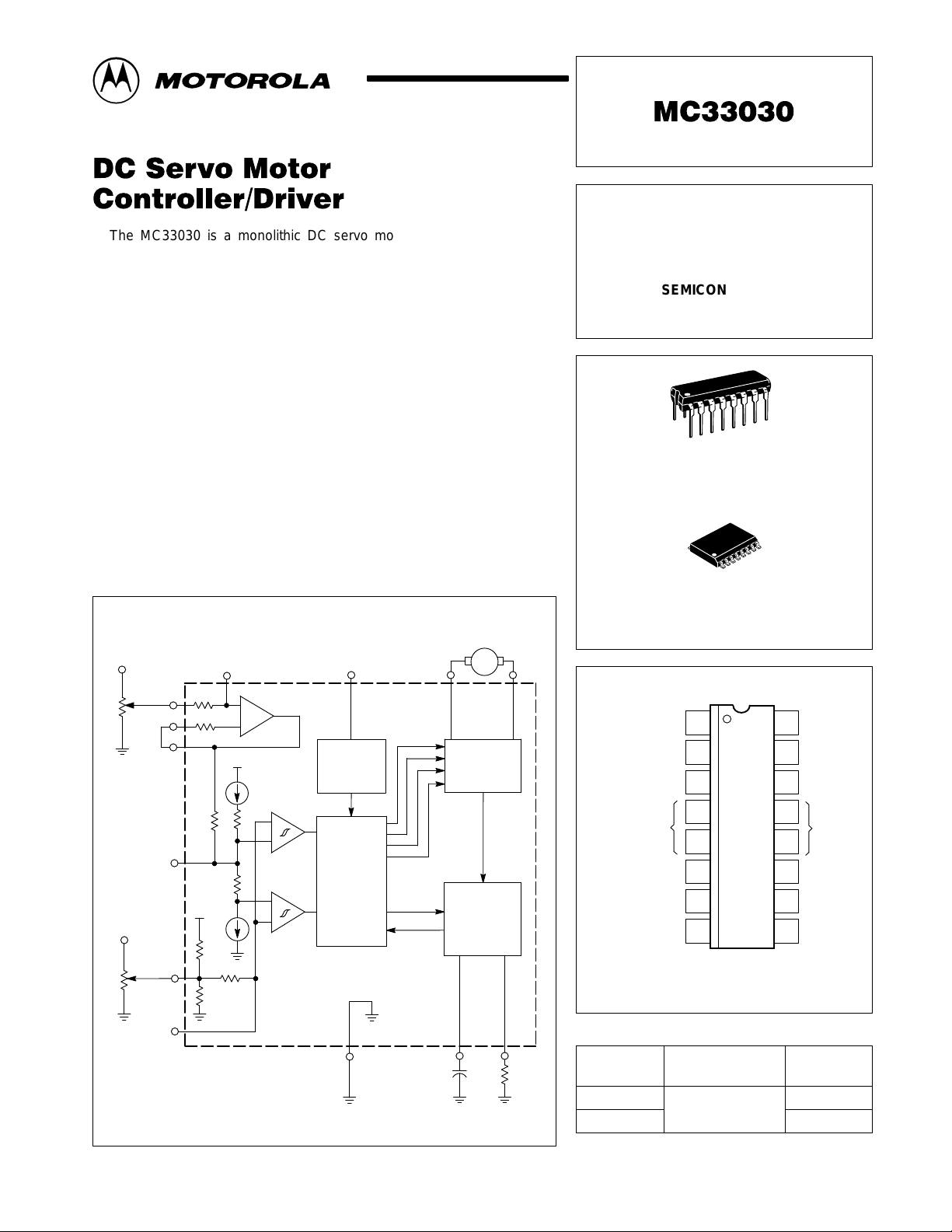
Representative Block Diagram
Motor
V
CC
Feedback
Position
V
CC
Reference
Position
9
8
7
6
3
+
1
2
Error Amp
+
–
+
+
–
Window
Detector
+
–
This device contains 119 active transistors.
V
CC
Over–
Voltage
Monitor
Drive/
Brake
Logic
Direction
Memory
4, 5, 12, 13
1011
Programmable
C
DLY
Power
H–Switch
Over–
Current
Detector
& Latch
14
1516
R
OC
DC SERVO MOTOR
CONTROLLER/DRIVER
SEMICONDUCTOR
TECHNICAL DATA
16
1
P SUFFIX
PLASTIC PACKAGE
CASE 648C
(DIP–16)
16
1
DW SUFFIX
PLASTIC PACKAGE
CASE 751G
(SOP–16L)
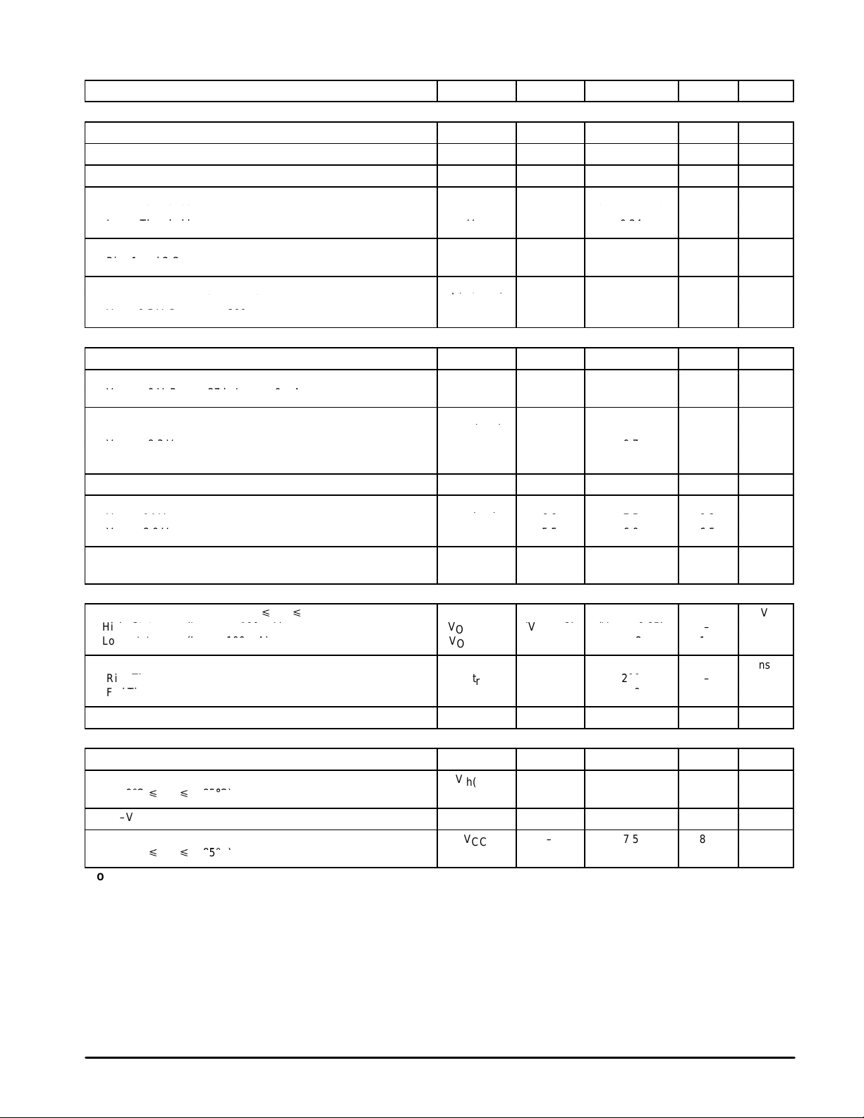
PIN CONNECTIONS
Reference
Reference
Input Filter
Error Amp Output
Filter/Feedback Input
Gnd
Error Amp
Error Amp
Inverting Input
Error Amp Non–
Inverting Input
Pins 4, 5, 12 and 13 are electrical ground and heat
sink pins for IC.
116
Input
2
3
4
5
6
Output
7
8
(Top View)
ORDERING INFORMATION
Operating
Device
MC33030DW
MC33030P
Temperature Range
TA = –40° to +85°C
Over–Current
Delay
Over–Current
15
Reference
Driver
14
Output A
13
Gnd
12
11
V
CC
Driver
10
Output B
Error Amp
9
Input Filter
Package
SOP–16L
DIP–16
MOTOROLA ANALOG IC DEVICE DATA
Motorola, Inc. 1996 Rev 2
1
MC33030
pgg
IR
CC
Ch
Su , ua e Case 6 8C
Th
R
15
(Pins 4, 5, 12, 13)
Thermal Resistance, Junction to Case
R
θJC
18
Input Bias Current (V
Pi
R
L
100 k)
I
IB
7.0
nA
MAXIMUM RATINGS
Rating Symbol Value Unit
Power Supply Voltage V
Input Voltage Range
Op Amp, Comparator, Current Limit
(Pins 1, 2, 3, 6, 7, 8, 9, 15)
Input Differential Voltage Range
Op Amp, Comparator (Pins 1, 2, 3, 6, 7, 8, 9)
Delay Pin Sink Current (Pin 16) I
Output Source Current (Op Amp) I
Drive Output Voltage Range (Note 1) V
Drive Output Source Current (Note 2) I
Drive Output Sink Current (Note 2) I
Brake Diode Forward Current (Note 2) I
Power Dissipation and Thermal
aracteristics
P Suffix, Dual In Line Case 648C
Thermal Resistance, Junction–to–Air
ermal Resistance, Junction–to–Case
(Pins 4, 5, 12, 13)
DW Suffix, Dual In Line Case 751G
Thermal Resistance, Junction–to–Air
Thermal Resistance, Junction–to–Case
(Pins 4, 5, 12, 13)
Operating Junction Temperature T
Operating Ambient Temperature Range T
Storage Temperature Range T
NOTES: 1.The upper voltage level is clamped by the forward drop, VF, of the brake diode.
2. These values are for continuous DC current. Maximum package power dissipation limits must
be observed.
CC
V
IR
V
IDR
DLY(sink)
source
DRV
DRV(source)
DRV(sink)
F
R
θJA
θJC
R
θJA
R
J
A
stg
–0.3 to (VCC + VF) V
36 V
–0.3 to V
–0.3 to V
20 mA
10 mA
1.0 A
1.0 A
1.0 A
80
94
18
+150 °C
–40 to +85 °C
–65 to +150 °C
CC
CC
V
V
°C/W
ELECTRICAL CHARACTERISTICS (V
Characteristic
ERROR AMP
Input Offset Voltage (– 40°C p TA p 85°C)
V
= 7.0 V, RL = 100 k
Pin 6
Input Offset Current (V
Input Common–Mode Voltage Range
∆VIO = 20 mV, RL = 100 k
Slew Rate, Open Loop (VID = 0.5 V, CL = 15 pF) SR – 0.40 – V/µs
Unity–Gain Crossover Frequency f
Unity–Gain Phase Margin φm – 63 – deg.
Common–Mode Rejection Ratio (V
Power Supply Rejection Ratio
VCC = 9.0 to 16 V, V
Output Source Current (V
Output Sink Current (V
Output Voltage Swing (RL = 17 k to Ground) V
NOTES: 3.The upper or lower hysteresis will be lost when operating the Input, Pin 3, close to the respective rail. Refer to Figure 4.
4.Low duty cycle pulse techniques are used during test to maintain junction temperature as close to ambient temperature as possible.
= 1.0 V, RL = 100 k) I
Pin 6
=
6 = 7.0 V,
n
Pin 6
= 7.0 V, RL = 100 k
Pin 6
= 12 V) IO
Pin 6
= 1.0 V) IO
Pin 6
= 14 V, TA = 25°C, unless otherwise noted.)
CC
Symbol Min Typ Max Unit
V
IO
IO
=
=
V
ICR
c
= 7.0 V, RL = 100 k) CMRR 50 82 – dB
PSRR – 89 – dB
+
–
OH
V
OL
– 1.5 10 mV
– 0.7 – nA
–
–
– 0 to (VCC – 1.2) – V
– 550 – kHz
– 1.8 – mA
– 250 – µA
12.5
–
13.1
0.02
–
–
–
–
V
V
2
MOTOROLA ANALOG IC DEVICE DATA
MC33030
pg()
pg y
p(IN/DRV)
µ
()
y(
OC DRV
)
DLY(sink)
th(OC)
p(
A
)
()
pg g(
L
p)
()
ELECTRICAL CHARACTERISTICS (continued) (V
Characteristic
WINDOW DETECTOR
Input Hysteresis Voltage (V1 – V4, V2 – V3, Figure 18) V
Input Dead Zone Range (V2 – V4, Figure 18) V
Input OffsetV oltage ([V2 – V
Input Functional Common–Mode Range (Note 3)
Upper Threshold
Lower Threshold V
Reference Input Self Centering Voltage
Pins 1 and 2 Open
Window Detector Propagation Delay
Comparator Input, Pin 3, to Drive Outputs
VID = 0.5 V, R
OVER–CURRENT MONITOR
Over–Current Reference Resistor Voltage (Pin 15) R
Delay Pin Source Current
V
= 0 V, ROC = 27 k, I
DLY
Delay Pin Sink Current (ROC = 27 k, I
V
= 5.0 V
DLY
V
= 8.3 V
DLY
V
= 14 V – 16.5 –
DLY
Delay Pin Voltage, Low State (I
Over–Current Shutdown Threshold
VCC = 14 V
VCC = 8.0 V 5.5 6.0 6.5
Over–Current Shutdown Propagation Delay
Delay Capacitor Input, Pin 16, to Drive Outputs, VID = 0.5 V
L(DRV)
= 390 Ω
] – [V
Pin 2
= 0 mA
DRV
= 0 mA) V
DLY
– V4] Figure 18) V
Pin 2
= 0 mA)
DRV
= 14 V, TA = 25°C, unless otherwise noted.)
CC
Symbol Min Typ Max Unit
H
IDZ
IO
V
IH
IL
V
RSC
t
p(IN/DRV)
OC
I
DLY(source)
I
DLY(sink)
OL(DLY)
V
th(OC)
t
p(DLY/DRV)
25 35 45 mV
166 210 254 mV
– 25 – mV
– (VCC – 1.05)
– 0.24 –
– (1/2 VCC) – V
– 2.0 – µs
3.9 4.3 4.7 V
– 5.5 6.9 µA
– 0.1
– 0.7
– 0.3 0.4 V
6.8
– 1.8 – µs
7.5
–
V
mA
–
–
V
8.2
POWER H–SWITCH
Drive–Output Saturation (– 40°C p TA p+ 85°C, Note 4)
High–State (I
Low–State (I
Drive–Output Voltage Switching T ime (CL = 15 pF)
Rise Time
Fall Time t
Brake Diode Forward Voltage Drop (IF = 200 mA, Note 4) V
TOTAL DEVICE
Standby Supply Current I
Over–Voltage Shutdown Threshold
(– 40°C p TA p + 85°C)
Over–Voltage Shutdown Hysteresis (Device “off” to “on”) V
Operating Voltage Lower Threshold
(– 40°C p TA p + 85°C)
NOTES: 3. The upper or lower hysteresis will be lost when operating the Input, Pin 3, close to the respective rail. Refer to Figure 4.
4.Low duty cycle pulse techniques are used during test to maintain junction temperature as close to ambient temperature as possible.
source
= 100 mA)
sink
= 100 mA)
V
OH(DRV)
V
OL(DRV)
t
r
f
F
CC
V
th(OV)
H(OV)
V
CC
(VCC – 2) (VCC – 0.85)
– 0.12 1.0
– 200
– 200 –
– 1.04 2.5 V
– 14 25 mA
16.5 18 20.5 V
0.3 0.6 1.0 V
– 7.5 8.0 V
–
V
ns
–
MOTOROLA ANALOG IC DEVICE DATA
3
MC33030
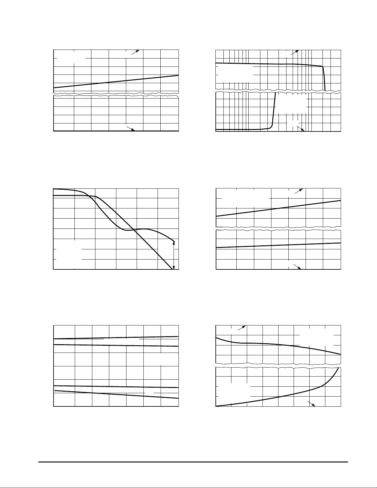
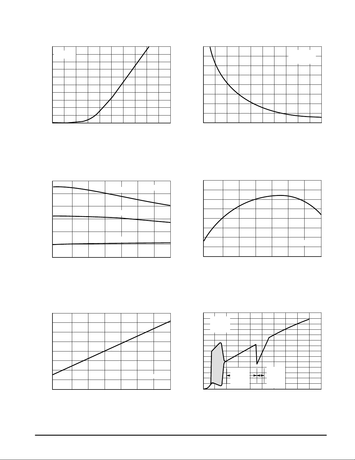
Figure 1. Error Amp Input Common–Mode
V oltage Range versus Temperature
0
∆
VIO = 20 mV
RL = 100 k
– 400
– 800
800
400
, INPUT COMMON–MODE RANGE (mV)
ICR
V
0
– 55
TA, AMBIENT TEMPERATURE (°C)
25 3.0 k100 1.0 k300
Figure 3. Open Loop V oltage Gain and
Phase versus Frequency
80
60
40
VCC = 14
V
= 7.0 V
20
out
RL = 100 k
, OPEN–LOOP VOLTAGE GAIN (dB)
CL = 40 pF
VOL
A
0
1.0 10 100 10 k 100 k 1.0 M1.0 k
TA = 25
°
C
Phase
f, FREQUENCY (Hz)
Gnd
V
CC
Gain
10050 750– 25
Phase
Margin
= 63
Figure 2. Error Amp Output Saturation
versus Load Current
125
0
– 1.0
Source Saturation
RL to Gnd
TA = 25
– 2.0
2.0
1.0
, OUTPUT SA TURATION VOLTAGE (V)
sat
V
0
30
°
C
IL, LOAD CURRENT (
V
CC
Sink Saturation
RL to VCC
°
C
TA = 25
Gnd
± µ
A)
Figure 4. Window Detector Reference–Input
Common–Mode V oltage Range
versus T emperature
0
45
90
135
°
, EXCESS PHASE (DEGREES)
φ
180
0
Max. Pin 2 V
Pin 3 can change
– 0.5
state of drive outputs.
– 1.0
– 1.5
0.3
0.2
, INPUT COMMON–MODE RANGE (V)
0.1
ICR
V
0
– 55
– 25
so that
ICR
0 255075100
TA, AMBIENT TEMPERATURE (
V
CC
Gnd
125
°
C)
Figure 5. Window Detector Feedback–Input
Thresholds versus T emperature
7.15
7.10
7.05
7.00
6.95
, FEEDBACK–INPUT VOLTAGE (V)
6.90
FB
V
6.85
– 55 – 25 125
TA, AMBIENT TEMPERATURE (
Upper Hysteresis
Lower Hysteresis
0 25 50 75 100
V
2
V
3
VCC = 14 V
Pin 2 = 7.00 V
V
1
V
4
°
C)
4
Figure 6. Output Driver Saturation
versus Load Current
0
V
CC
– 1.0
1.0
Sink Saturation
, OUTPUT SA TURATION VOLTAGE (V)
V
RL = VCC
°
C
TA = 25
sat
0
0 200 400 600 800
IL, LOAD CURRENT (±mA)
Source Saturation
RL to Gnd
TA = 25
Gnd
MOTOROLA ANALOG IC DEVICE DATA
°
C
MC33030
, FORWARD CURRENT (mA)
F
I
500
400
300
200
100
600
400
Figure 7. Brake Diode Forward Current
versus Forward Voltage
TA = 25°C
0
VF, FORWARD VOLTAGE (V)
1.10.90.70.5
Figure 9. Output Source Current–Limit
versus T emperature
ROC = 15 k
ROC = 27 k
1.3
VCC = 14 V
1.5
, OUTPUT SOURCE CURRENT (mA)
source
I
1.04
1.00
0.96
Figure 8. Output Source Current–Limit versus
Over–Current Reference Resistance
800
VCC = 14 V
TA = 25
600
400
200
0
ROC, OVER–CURRENT REFERENCE RESISTANCE (k
Figure 10. Normalized Delay Pin Source
Current versus Temperature
°
C
806040020
100
Ω
)
200
, OUTPUT SOURCE CURRENT (mA)
source
I
0
– 55
TA, AMBIENT TEMPERATURE (°C)
Figure 11. Normalized Over–Current Delay
Threshold V oltage versus Temperature
1.04
1.02
1.00
(NORMALIZED)
0.98
, OVER–CURRENT DELAY THRESHOLD VOLTAGE
0.96
th(OC)
V
0– 25
TA, AMBIENT TEMPERATURE (
ROC = 68 k
25
VCC = 14 V
75 1005025– 55
°
C)
12575500– 25 100
125
(NORMALIZED)
, DELAY PIN SOURCE CURRENT
0.92
DLY(source)
0.88
I
– 55 12525 50 10075
– 25 0
TA, AMBIENT TEMPERATURE (
Figure 12. Supply Current versus
Supply V oltage
28
Pins 6 to 7
Pins 2 to 8
, SUPPLY CURRENT (mA)
CC
I
24
20
16
12
8.0
4.0
0
°
C
TA = 25
Minimum
Operating
Voltage
Range
8.0016
VCC, SUPPLY VOLTAGE (V)
Over–
Voltage
Shutdown
Range
24
VCC = 14 V
°
C)
32 40
MOTOROLA ANALOG IC DEVICE DATA
5
 Loading...