

SEMICONDUCTOR
TECHNICAL DATA
VOLTAGE REGULATOR
ORDERING INFORMATION
Order this document by MC1723C/D
P SUFFIX
PLASTIC PACKAGE
CASE 646
D SUFFIX
PLASTIC PACKAGE
CASE 751A
(SO–14)
Device
Operating
Temperature
Range
Package
MC1723CD
MC1723CP
TA = 0° to +70°C
SO–14
Plastic DIP
Alternate
LM723CN
µA723PC
–
1
MOTOROLA ANALOG IC DEVICE DATA
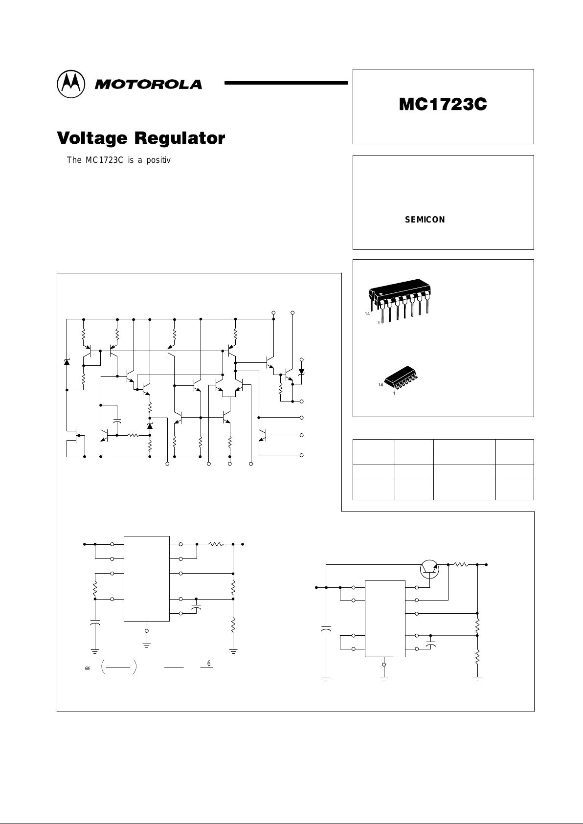
The MC1723C is a positive or negative voltage regulator designed to
deliver load current to 150 mAdc. Output current capability can be increased
to several amperes through use of one or more external pass transistors.
MC1723C is specified for operation over the commercial temperature range
(0° to +70°C).
• Output Voltage Adjustable from 2.0 Vdc to 37 Vdc
• Output Current to 150 mAdc Without External Pass Transistors
• 0.01% Line and 0.03% Load Regulation
• Adjustable Short Circuit Protection
Figure 1. Representative Schematic Diagram
Figure 2. Typical Circuit Connection
Figure 3. Typical NPN Current Boost Connection
Noninverting
Input
Inverting
Input
V
EE
475
Current
Sense
Current
Limit
Compensation
V
O
6.2V
V
z
9
1.0k
25k
500
5.0pF
150
20k
300
30k
100
15k
6V
ref
10
13
2
3
V
CC
V
C
1112
15k
1.0k
6.2V
6.2V
5.0k
V
in
12
11
6
5
C
ref
R3
(7 < VO < 37)
MC1723C
10
2
3
4
C1
100pF
13
7
R
SC
R1
R2
For best results 10 k < R2 < 100 k
For minimum drift R3 = R1 | | R2
VO
^
7I
SC
=
R1 + R2
R2
V
sense
0.66
R
SC
V
O
= at TJ = + 25°C
Vin = 20Vdc
RSC = 0.33
VO = +15Vdc
IL = 2Adc max
12k
10k
4
C1
13
3
2
1012
11
6
5
7
MC1723C
0.1
µ
F
2N3055 or Equiv
100pF
R
SC
Motorola, Inc. 1996 Rev 5
MC1723C
2
MOTOROLA ANALOG IC DEVICE DATA
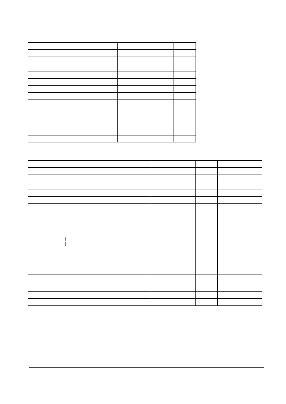
MAXIMUM RATINGS
(TA = +25°C, unless otherwise noted.)
Rating Symbol Value Unit
Pulse Voltage from VCC to VEE (50 ms) V
I(p)
50 V
pk
Continuous Voltage from VCC to V
EE
V
I
40 Vdc
Input–Output Voltage Differential VI–V
O
40 Vdc
Maximum Output Current I
L
150 mAdc
Current from V
ref
I
ref
15 mAdc
Current from V
z
I
z
25 mA
Voltage Between Noninverting Input and V
EE
V
ie
8.0 Vdc
Differential Input Voltage V
id
±5.0 Vdc
Power Dissipation and Thermal Characteristics
TA = +25°C
Derate above TA = +25°C
Thermal Resistance, Junction–to–Air
P
D
1/θ
JA
θ
JA
1.25
10
100
W
mW/°C
°C/W
Operating and Storage Junction T emperature Range TJ, T
stg
–65 to +175 °C
Operating Ambient Temperature Range T
A
0 to +70 °C
ELECTRICAL CHARACTERISTICS (T
A
= +25°C, Vin 12 Vdc, VO = 5.0 Vdc, IL = 1.0 mAdc, RSC = 0, C1 = 100 pF, C
ref
= 0 and divider
impedance as seen by the error amplifier ≤ 10 kΩ connected as shown in Figure 2, unless otherwise noted.)
Characteristics
Symbol Min Typ Max Unit
Input Voltage Range V
I
9.5 – 40 Vdc
Output Voltage Range V
O
2.0 – 37 Vdc
Input–Output Voltage Differential VI–V
O
3.0 – 38 Vdc
Reference Voltage V
ref
6.80 7.15 7.50 Vdc
Standby Current Drain ( IL = 0, Vin = 30 V) I
IB
– 2.3 4.0 mAdc
Output Noise Voltage (f = 100 Hz to 10 kHz)
C
ref
= 0
C
ref
= 5.0 µF
V
n
–
–
20
2.5
–
–
µV(RMS)
Average Temperature Coefficient of Output
Voltage (T
low
< TA < T
high
)
TCV
O
– 0.003 0.015 %/°C
Line Regulation
(TA = 25°C)
12 V < Vin < 15 V
12 V < Vin < 40 V
(T
low
< TA < T
high
)
12 V < Vin < 15 V
Reg
line
–
–
–
0.01
0.1
–
0.1
0.5
0.3
% V
O
Load Regulation (1.0 mA < IL < 50 mA)
TA = 25°C
T
low
< TA < T
high
Reg
load
–
–
0.03
–
0.2
0.6
% V
O
Ripple Rejection (f = 50 Hz to 10 kHz)
C
ref
= 0
C
ref
= 5.0 µF
RR
–
–
74
86
–
–
dB
Short Circuit Current Limit (RSC = 10 Ω, VO = 0) I
SC
– 65 – mAdc
Long Term Stability ^VO/^t – 0.1 – %/1000 Hr .
NOTE: T
low
to T
high
= 0° to +70°C
MC1723C
3
MOTOROLA ANALOG IC DEVICE DATA
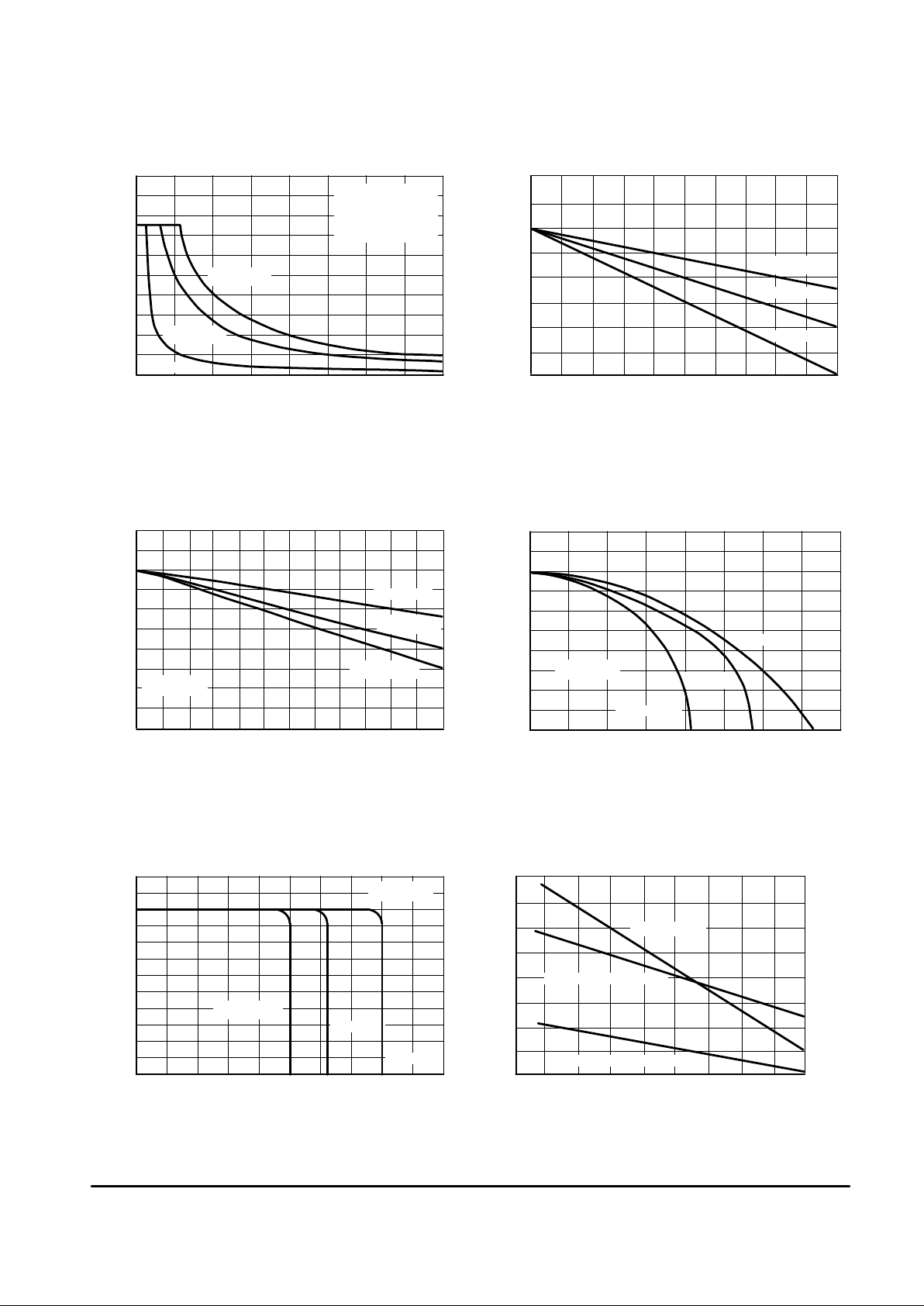
Figure 4. Maximum Load Current as a Function
of Input–Output Voltage Differential
Figure 5. Load Regulation Characteristics
Without Current Limiting
Figure 6. Load Regulation Characteristics
With Current Limiting
Figure 7. Load Regulation Characteristics
With Current Limiting
Figure 8. Current Limiting Characteristics
Figure 9. Current Limiting Characteristics
as a Function of Junction Temperature
Vin–V
out
, INPUT–OUTPUT VOLTAGE (V)
(max), LOAD CURRENT (mA)
L
0 10203040
I
T
A
= + 125°C
IO, OUTPUT CURRENT (mA)
, LOAD REGULATION (%V
load O
0 2040 6080100
)Reg
TA = + 125°C
TA = –55°C
, LOAD REGULATION (%V
load O
)Reg
IO, OUTPUT CURRENT (mA)
0 5.0 10 15 20 25 30
TA = –55°C
, LOAD REGULATION (%V
load O
)Reg
IO, OUTPUT CURRENT (mA)
020406080
T
A
= +125°C
TA = –55°C
IO, OUTPUT CURRENT (mA)
RELATIVE OUTPUT VOLTAGE (V)
0 20406080100
T
A
=+25°C
TA = –55°C
TJ, JUNCTION TEMPERATURE (°C)
CURRENT LIMIT SENSE VOLTAGE (V)
–50 0 50 100 150
40
80
120
160
200
LIMITING CURRENT (mA)
Sense Voltage
Limit Current RSC = 5.0
Ω
Limit Current RSC = 10
Ω
0
40
80
120
160
200
–0.15
–0.1
–0.05
0
0.05
–0.15
–0.1
–0.05
0
0.05
–0.2 –0.4
–0.3
–0.2
–0.1
0
0.1
0
0.2
0.4
0.6
0.8
1.0
1.2
0.4
0.5
0.6
0.7
0.8
T
Jmax
= 150°C
RTH = 150
°
C/W
P
STANDBY
60 mW
(No heatsink)
TA = + 25°C
TA = + 75°C
TA = + 25°C
RSC = 10
Ω
TA = + 25°C
TA = + 125°C
RSC = 10
Ω
TA = +25°C
RSC = 10
Ω
TA = + 125°C

MC1723C
4
MOTOROLA ANALOG IC DEVICE DATA
Figure 10. Line Regulation as a Function
of Input–Output Voltage Differential
Figure 11. Load Regulation as a Function
of Input–Output Voltage Differential
Figure 12. Standby Current Drain as a
Function of Input Voltage
Figure 13. Line Transient Response
Figure 14. Load Transient Response
Figure 15. Output Impedance as
Function of Frequency
Vin–V
out
, INPUT–OUTPUT VOLTAGE (V)
, LINE REGULATION (%V
in O
5.0 15 25 35
∆
Vin = +3 V
Reg )
, LOAD REGULATION (%V
load O
)Reg
Vin–V
out
, INPUT–OUTPUT VOLTAGE (V)
0 1020304050
STANDBY CURRENT (mA)
Vin, INPUT VOLTAGE (V)
10 20 30 40
VO = V
ref
IL = 0
TA = –55°C
TA = +25°C
TA = +125°C
OUTPUT VOLTAGE DEVIATION (mV)
t, TIME (µs)
–5.0 0 10 20 30 40 45
0
2.0
4.0
INPUT VOL TAGE DEVIATION (V)
Input Voltage
Output Voltage
OUTPUT VOLTAGE DEVIATION (mV)
t, TIME (µs)
–5.0 0 10 20 30 40 45
0
10
LOAD DEVIATION (mA)
Load Current
Output Voltage
IL = 40 mA
f, FREQUENCY (Hz)
100 1.0 k 10 k 100 k 1 M
–0.1
0
0.1
0.2
–0.2
–0.1
0
0.1
0
1.0
2.0
3.0
4.0
–2.0
0
2.0
–8.0
–4.0
0
2.0
0.01
0.1
1.0
10
IL = 1.0 to IL = 50 mA
IL = 50 mA
CI = 0
CI = 1.0 µF
Z
O
Ω
, OUTPUT IMPEDANCE ( )

MC1723C
5
MOTOROLA ANALOG IC DEVICE DATA
Figure 16. Typical Connection for 2 < VO < 7 Figure 17. Foldback Connection
Figure 18. +5.0 V, 1.0 A Switching Regulator Figure 19. +5.0 V, 1.0 A High Efficiency Regulator
Figure 20. +15 V, 1.0 A Regulator with Remote Sense Figure 21. –15 V Negative Regulator
+V
in
12
11
6
5
R2
R1
C
ref
7
13
4
3
2
10
R
SC
V
out
R3
1000pF
For best results 10 k < R1 +R2 < 100 k
For minimum drift R3 = R1 R2
VO
^
7
R2
R1 + R2
ISC =
V
sense
0.66
RSC
^
at TJ = + 25°C
MC1723C
12
11
6
5
10
2
4
13
R
A
10k
R1
R2
3
7
100pF
V
out
R
SC
V
out
I
SC
I
L
I
knee
a
1–a
V
sense
Iknee
ISC
–1
RSC =
V
sense
(1–a) I
SC
+ V
in
RA = 10 kΩwhere a =
MC1723C
V
in
+10V
2.2k
1.0M
1.0k
5.1k
5
6
12
11
4
3
2
10 10
V
out
1N4001
or Equiv
1mH
2N4918 or Equiv
100
100
µ
F
7
0.1
µ
F
+
–
+5V
MC1723C
+6.5V
+10V
V
in1
V
in2
0.1
µ
F
12
11
3
10
2
4
13
1000pF
7
5
6
2.0k
5.1k
0.33
V
out
+5.0V
MC1723C
0.33
2N3055 or Equiv
10
2
3
4
100pF
13
10k
12k
+20V
+ Sense V
out
+15V
Load
– Sense
5
6
11
12
V
in
0.1
µ
F
7
MC1723C
V
ref
12
11
6
5
10
4
100pF
13
7
Vin = –20 V
V2 = 14V
2N3055
or Equiv
V
out
= –15 V
10
µ
F
12k
10k
–
+
V
ref
–
+
+
–
MC1723C
R
SC
V
O

MC1723C
6
MOTOROLA ANALOG IC DEVICE DATA
Figure 22. +12V, 1.0 A Regulator
(Using PNP Current Boost)
MC1723C
0.33
V
out
= +12 V+18V
V
in
100
12
11
6
5
10
2
3
4
13
100pF
10k
12k
7
2N3791
or Equiv

MC1723C
7
MOTOROLA ANALOG IC DEVICE DATA
OUTLINE DIMENSIONS
P SUFFIX
PLASTIC PACKAGE
CASE 646–06
ISSUE L
D SUFFIX
PLASTIC PACKAGE
CASE 751A–03
(SO–14)
ISSUE F
17
14 8
B
A
F
HG D
K
C
N
L
J
M
SEATING
PLANE
NOTES:
1. LEADS WITHIN 0.13 (0.005) RADIUS OF TRUE
POSITION AT SEATING PLANE AT MAXIMUM
MATERIAL CONDITION.
2. DIMENSION L TO CENTER OF LEADS WHEN
FORMED PARALLEL.
3. DIMENSION B DOES NOT INCLUDE MOLD
FLASH.
4. ROUNDED CORNERS OPTIONAL.
DIM MIN MAX MIN MAX
MILLIMETERSINCHES
A 0.715 0.770 18.16 19.56
B 0.240 0.260 6.10 6.60
C 0.145 0.185 3.69 4.69
D 0.015 0.021 0.38 0.53
F 0.040 0.070 1.02 1.78
G 0.100 BSC 2.54 BSC
H 0.052 0.095 1.32 2.41
J 0.008 0.015 0.20 0.38
K 0.115 0.135 2.92 3.43
L 0.300 BSC 7.62 BSC
M 0 10 0 10
N 0.015 0.039 0.39 1.01
____
NOTES:
1. DIMENSIONING AND TOLERANCING PER
ANSI Y14.5M, 1982.
2. CONTROLLING DIMENSION: MILLIMETER.
3. DIMENSIONS A AND B DO NOT INCLUDE
MOLD PROTRUSION.
4. MAXIMUM MOLD PROTRUSION 0.15 (0.006)
PER SIDE.
5. DIMENSION D DOES NOT INCLUDE DAMBAR
PROTRUSION. ALLOWABLE DAMBAR
PROTRUSION SHALL BE 0.127 (0.005) TOTAL
IN EXCESS OF THE D DIMENSION AT
MAXIMUM MATERIAL CONDITION.
–A–
–B–
G
P 7 PL
14 8
71
M
0.25 (0.010) B
M
S
B
M
0.25 (0.010) A
S
T
–T–
F
R X 45
SEATING
PLANE
D 14 PL
K
C
J
M
_
DIM MIN MAX MIN MAX
INCHESMILLIMETERS
A 8.55 8.75 0.337 0.344
B 3.80 4.00 0.150 0.157
C 1.35 1.75 0.054 0.068
D 0.35 0.49 0.014 0.019
F 0.40 1.25 0.016 0.049
G 1.27 BSC 0.050 BSC
J 0.19 0.25 0.008 0.009
K 0.10 0.25 0.004 0.009
M 0 7 0 7
P 5.80 6.20 0.228 0.244
R 0.25 0.50 0.010 0.019
____

MC1723C
8
MOTOROLA ANALOG IC DEVICE DATA
Motorola reserves the right to make changes without further notice to any products herein. Motorola makes no warranty , representation or guarantee regarding
the suitability of its products for any particular purpose, nor does Motorola assume any liability arising out of the application or use of any product or circuit, and
specifically disclaims any and all liability, including without limitation consequential or incidental damages. “T ypical” parameters which may be provided in Motorola
data sheets and/or specifications can and do vary in different applications and actual performance may vary over time. All operating parameters, including “Typicals”
must be validated for each customer application by customer’s technical experts. Motorola does not convey any license under its patent rights nor the rights of
others. Motorola products are not designed, intended, or authorized for use as components in systems intended for surgical implant into the body, or other
applications intended to support or sustain life, or for any other application in which the failure of the Motorola product could create a situation where personal injury
or death may occur. Should Buyer purchase or use Motorola products for any such unintended or unauthorized application, Buyer shall indemnify and hold Motorola
and its officers, employees, subsidiaries, affiliates, and distributors harmless against all claims, costs, damages, and expenses, and reasonable attorney fees
arising out of, directly or indirectly, any claim of personal injury or death associated with such unintended or unauthorized use, even if such claim alleges that Motorola
was negligent regarding the design or manufacture of the part. Motorola and are registered trademarks of Motorola, Inc. Motorola, Inc. is an Equal
Opportunity/Affirmative Action Employer.
Mfax is a trademark of Motorola, Inc.
How to reach us:
USA/EUROPE/ Locations Not Listed: Motorola Literature Distribution; JAPAN: Motorola Japan Ltd.; SPD, Strategic Planning Office, 141,
P.O. Box 5405, Denver, Colorado 80217. 1–303–675–2140 or 1–800–441–2447 4–32–1 Nishi–Gotanda, Shinagawa–ku, T okyo, Japan. 81–3–5487–8488
Customer Focus Center: 1–800–521–6274
Mfax: RMFAX0@email.sps.mot.com – TOUCHTONE 1–602–244–6609 ASIA/PACIFIC: Motorola Semiconductors H.K. Ltd.; Silicon Harbour Centre,
Motorola Fax Back System – US & Canada ONLY 1–800–774–1848 2, Dai King Street, Tai Po Industrial Estate, Tai Po, N.T., Hong Kong.
– http://sps.motorola.com/mfax/ 852–26629298
HOME PAGE: http://motorola.com/sps/
MC1723C/D
◊
 Loading...