

SEMICONDUCTOR TECHNICAL DATA
Advance Information
Order this document
by MC14LC5480/D
The MC14LC5480 is a general purpose per channel PCM Codec–Filter with
pin selectable Mu–Law or A–Law companding, and is offered in 20–pin DIP,
SOG, and SSOP packages. This device performs the voice digitization and
reconstruction as well as the band limiting and smoothing required for PCM
systems. This device is designed to operate in both synchronous and
asynchronous applications and contains an on–chip precision reference
voltage.
This device has an input operational amplifier whose output is the input to the
encoder section. The encoder section immediately low–pass filters the analog
signal with an active R–C filter to eliminate very high frequency noise from being
modulated down to the passband by the switched capacitor filter. From the
active R–C filter, the analog signal is converted to a dif ferential signal. From this
point, all analog signal processing is done differentially. This allows processing
of an analog signal that is twice the amplitude allowed by a single–ended
design, which reduces the significance of noise to both the inverted and
non–inverted signal paths. Another advantage of this differential design is that
noise injected via the power supplies is a common–mode signal that is
cancelled when the inverted and non–inverted signals are recombined. This
dramatically improves the power supply rejection ratio.
After the differential converter, a differential switched capacitor filter band–
passes the analog signal from 200 Hz to 3400 Hz before the signal is digitized
by the differential compressing A/D converter .
The decoder accepts PCM data and expands it using a differential D/A
converter. The output of the D/A is low–pass filtered at 3400 Hz and sinX/X
compensated by a differential switched capacitor filter. The signal is then filtered
by an active R–C filter to eliminate the out–of–band energy of the switched
capacitor filter.
The MC14LC5480 PCM Codec–Filter accepts a variety of clock formats,
including Short Frame Sync, Long Frame Sync, IDL, and GCI timing
environments. This device also maintains compatibility with Motorola’s family of
Telecommunication products, including the MC14LC5472 U–Interface Transceiver, MC145474/75 S/T–Interface Transceiver, MC145532 ADPCM Transcoder, MC145422/26 UDLT–1, MC145421/25 UDLT–2, and MC3419/MC33120
SLIC.
The MC14LC5480 PCM Codec–Filter utilizes CMOS due to its reliable
low–power performance and proven capability for complex analog/digital VLSI
functions.
• Pin for Pin Replacement for the MC145480
• Single 5 V Power Supply
• Typical Power Dissipation of 15 mW, Power–Down of 0.01 mW
• Fully–Differential Analog Circuit Design for Lowest Noise
• Transmit Band–Pass and Receive Low–Pass Filters On–Chip
• Active R–C Pre–Filtering and Post–Filtering
• Mu–Law and A–Law Companding by Pin Selection
• On–Chip Precision Reference Voltage (1.575 V)
• Push–Pull 300 Ω Power Drivers with External Gain Adjust
• MC145536EVK is the Evaluation Kit that Also Includes the MC145532
ADPCM Transcoder
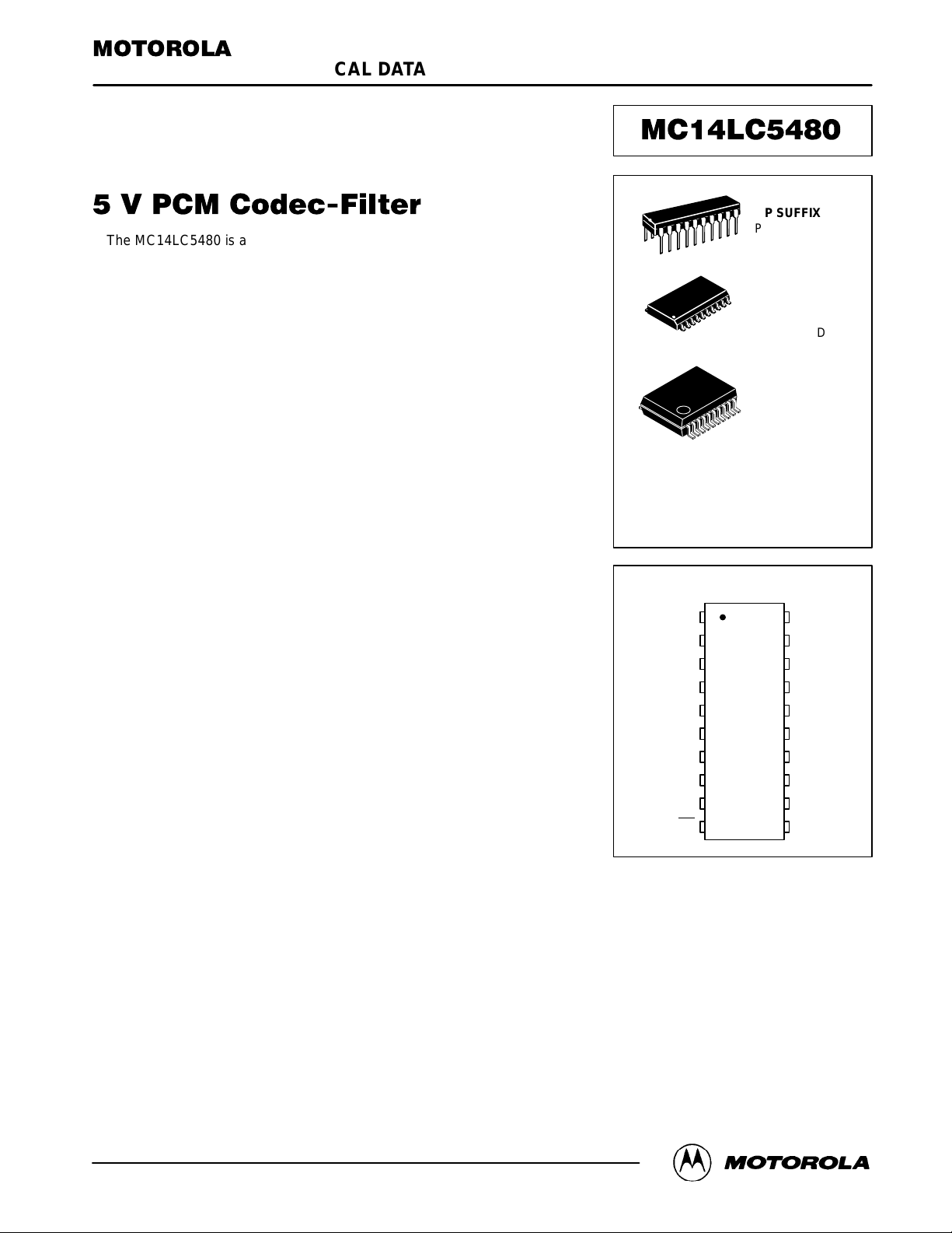
P SUFFIX
PLASTIC DIP
20
1
20
1
20
1
CASE 738
DW SUFFIX
SOG PACKAGE
CASE 751D
SD SUFFIX
SSOP
CASE 940C
ORDERING INFORMATION
MC14LC5480P Plastic DIP
MC14LC5480DW SOG Package
MC14LC5480SD SSOP
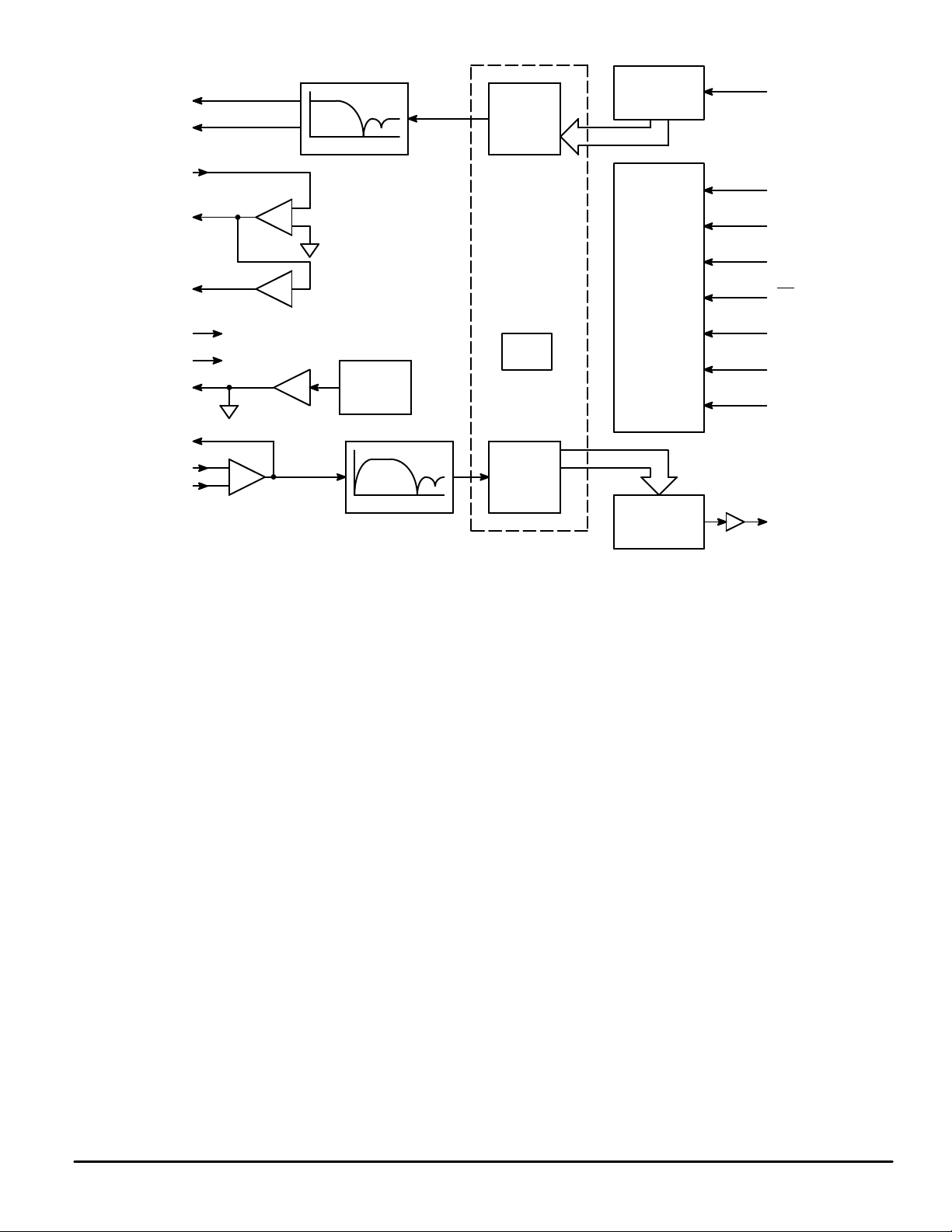
PIN ASSIGNMENT
RO+
RO–
PI
PO–
PO+ 5
V
DD
FSR
DR
BCLKR
PDI
1
2
3
4
6
7
8
9
10
20
19
18
17
16
15
14
13
12
11
V
AG
TI+
TI–
TG
Mu/A
V
SS
FST
DT
BCLKT
MCLK
This document contains information on a new product. Specifications and information herein are subject to change without notice.
REV 0.1
5/96
Motorola, Inc. 1996
MC14LC5480MOTOROLA
1
RO+
RO–
PO–
PO+
V
DD
V
SS
V
AG
TG
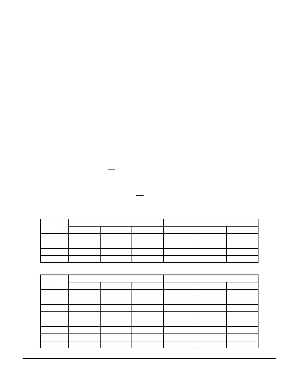
RECEIVE
SHIFT
DAC
FREQ
PI
–
– 1
+
1
2.4 V
REFERENCE
SHARED
DAC
1.575 V
REF
REGISTER
SEQUENCE
AND
CONTROL
DR
FSR
BCLKR
Mu/A
PDI
MCLK
BCLKT
FST
TI–
TI+
–
+
FREQ
Figure 1. MC14LC5480 PCM Codec–Filter Block Diagram
DEVICE DESCRIPTION
A PCM Codec–Filter is used for digitizing and reconstructing the human voice. These devices are used primarily for
the telephone network to facilitate voice switching and transmission. Once the voice is digitized, it may be switched by
digital switching methods or transmitted long distance (T1,
microwave, satellites, etc.) without degradation. The name
codec is an acronym from ‘‘COder’’ for the analog–to–digital
converter (ADC) used to digitize voice, and ‘‘DECoder’’ for
the digital–to–analog converter (DAC) used for reconstructing voice. A codec is a single device that does both the ADC
and DAC conversions.
To digitize intelligible voice requires a signal–to–distortion
ratio of about 30 dB over a dynamic range of about 40 dB.
This may be accomplished with a linear 13–bit ADC and
DAC, but will far exceed the required signal–to–distortion
ratio at larger amplitudes than 40 dB below the peak amplitude. This excess performance is at the expense of data per
sample. Two methods of data reduction are implemented by
compressing the 13–bit linear scheme to companded
pseudo–logarithmic 8–bit schemes. The two companding
schemes are: Mu–255 Law, primarily in North America and
Japan; and A–Law, primarily used in Europe. These companding schemes are accepted world wide. These companding schemes follow a segmented or ‘‘piecewise–linear’’ curve
formatted as sign bit, three chord bits, and four step bits. For
a given chord, all sixteen of the steps have the same voltage
weighting. As the voltage of the analog input increases, the
four step bits increment and carry to the three chord bits
ADC
TRANSMIT
SHIFT
REGISTER
DT
which increment. When the chord bits increment, the step
bits double their voltage weighting. This results in an effective resolution of six bits (sign + chord + four step bits) across
a 42 dB dynamic range (seven chords above 0, by 6 dB per
chord).
In a sampling environment, Nyquist theory says that to
properly sample a continuous signal, it must be sampled at a
frequency higher than twice the signal’s highest frequency
component. Voice contains spectral energy above 3 kHz, but
its absence is not detrimental to intelligibility. To reduce the
digital data rate, which is proportional to the sampling rate, a
sample rate of 8 kHz was adopted, consistent with a bandwidth of 3 kHz. This sampling requires a low–pass filter to
limit the high frequency energy above 3 kHz from distorting
the in–band signal. The telephone line is also subject to
50/60 Hz power line coupling, which must be attenuated
from the signal by a high–pass filter before the analog–to–
digital converter.
The digital–to–analog conversion process reconstructs a
staircase version of the desired in–band signal, which has
spectral images of the in–band signal modulated about the
sample frequency and its harmonics. These spectral images
are called aliasing components, which need to be attenuated
to obtain the desired signal. The low–pass filter used to attenuate these aliasing components is typically called a reconstruction or smoothing filter.
The MC14LC5480 PCM Codec–Filter has the codec, both
presampling and reconstruction filters, a precision voltage
reference on–chip, and requires no external components.
MC14LC5480 MOTOROLA
2

PIN DESCRIPTIONS
POWER SUPPLY
V
DD
Positive Power Supply (Pin 6)
This is the most positive power supply and is typically con-
nected to + 5 V. This pin should be decoupled to VSS with a
0.1 µF ceramic capacitor.
V
SS
Negative Power Supply (Pin 15)
This is the most negative power supply and is typically
connected to 0 V.
V
AG
Analog Ground Output (Pin 20)
This output pin provides a mid–supply analog ground reg-
ulated to 2.4 V. This pin should be decoupled to VSS with a
0.01 µF to 0.1 µF ceramic capacitor. All analog signal processing within this device is referenced to this pin. If the audio signals to be processed are referenced to VSS, then
special precautions must be utilized to avoid noise between
VSS and the VAG pin. Refer to the applications information in
this document for more information. The VAG pin becomes
high impedance when this device is in the powered down
mode.
CONTROL
Mu/A
Mu/A Law Select (Pin 16)
This pin controls the compression for the encoder and the
expansion for the decoder. Mu–Law companding is selected
when this pin is connected to VDD and A–Law companding is
selected when this pin is connected to VSS.
PDI
Power–Down Input (Pin 10)
This pin puts the device into a low power dissipation mode
when a logic 0 is applied. When this device is powered down,
all of the clocks are gated off and all bias currents are turned
off, which causes RO+, RO–, PO–, PO+, TG, VAG, and DT to
become high impedance. The device will operate normally
when a logic 1 is applied to this pin. The device goes through
a power–up sequence when this pin is taken to a logic 1
state, which prevents the DT PCM output from going low impedance for at least two FST cycles. The filters must settle
out before the DT PCM output or the RO+ or RO– receive
analog outputs will represent a valid analog signal.
ANALOG INTERFACE
TI+
Transmit Analog Input (Non–Inverting) (Pin 19)
This is the non–inverting input of the transmit input gain
setting operational amplifier . This pin accommodates a differential to single–ended circuit for the input gain setting op
amp. This allows input signals that are referenced to the V
pin to be level shifted to the VAG pin with minimum noise.
This pin may be connected to the VAG pin for an inverting
amplifier configuration if the input signal is already referenced to the VAG pin. The common mode range of the TI+
and TI– pins is from 1.2 V, to VDD minus 2 V. This is an FET
gate input. Connecting the TI+ pin to VDD will place this am-
SS
plifier’s output (TG) into a high–impedance state, thus allowing the TG pin to serve as a high–impedance input to the
transmit filter.
TI–
Transmit Analog Input (Inverting) (Pin 18)
This is the inverting input of the transmit gain setting operational amplifier. Gain setting resistors are usually connected from this pin to TG and from this pin to the analog
signal source. The common mode range of the TI+ and TI–
pins is from 1.2 V to VDD – 2 V. This is an FET gate input.
Connecting the TI+ pin to VDD will place this amplifier’s output (TG) into a high–impedance state, thus allowing the TG
pin to serve as a high–impedance input to the transmit filter.
TG
Transmit Gain (Pin 17)
This is the output of the transmit gain setting operational
amplifier and the input to the transmit band–pass filter. This
op amp is capable of driving a 2 kΩ load. Connecting the TI+
pin to VDD will place this amplifier’s output (TG) into a high–
impedance state, thus allowing the TG pin to serve as a
high–impedance input to the transmit filter. All signals at this
pin are referenced to the VAG pin. This pin is high impedance
when the device is in the powered down mode.
RO+
Receive Analog Output (Non–Inverting) (Pin 1)
This is the non–inverting output of the receive smoothing
filter from the digital–to–analog converter. This output is
capable of driving a 2 kΩ load to 1.575 V peak referenced to
the VAG pin. This pin is high impedance when the device is in
the powered down mode.
RO–
Receive Analog Output (Inverting) (Pin 2)
This is the inverting output of the receive smoothing filter
from the digital–to–analog converter. This output is capable
of driving a 2 kΩ load to 1.575 V peak referenced to the V
pin. This pin is high impedance when the device is in the
powered down mode.
PI
Power Amplifier Input (Pin 3)
This is the inverting input to the PO– amplifier. The non–
inverting input to the PO– amplifier is internally tied to the
VAG pin. The PI and PO – pins are used with external resistors in an inverting op amp gain circuit to set the gain of the
PO+ and PO– push–pull power amplifier outputs. Connecting PI to VDD will power down the power driver amplifiers and
the PO+ and PO– outputs will be high impedance.
PO–
Power Amplifier Output (Inverting) (Pin 4)
This is the inverting power amplifier output, which is used
to provide a feedback signal to the PI pin to set the gain of
the push–pull power amplifier outputs. This pin is capable of
driving a 300 Ω load to PO+. The PO+ and PO– outputs are
differential (push–pull) and capable of driving a 300 Ω load to
3.15 V peak, which is 6.3 V peak–to–peak. The bias voltage
and signal reference of this output is the VAG pin. The V
pin cannot source or sink as much current as this pin, and
AG
AG
MC14LC5480MOTOROLA
3

therefore low impedance loads must be between PO+ and
PO–. Connecting PI to VDD will power down the power driver
amplifiers and the PO+ and PO– outputs will be high impedance. This pin is also high impedance when the device is
powered down by the PDI
PO+
Power Amplifier Output (Non–Inverting) (Pin 5)
This is the non–inverting power amplifier output, which is
an inverted version of the signal at PO–. This pin is capable
of driving a 300 Ω load to PO–. Connecting PI to VDD will
power down the power driver amplifiers and the PO+ and
PO– outputs will be high impedance. This pin is also high impedance when the device is powered down by the PDI
See PI and PO– for more information.
DIGITAL INTERFACE
MCLK
Master Clock (Pin 11)
This is the master clock input pin. The clock signal applied
to this pin is used to generate the internal 256 kHz clock and
sequencing signals for the switched–capacitor filters, ADC,
and DAC. The internal prescaler logic compares the clock on
this pin to the clock at FST (8 kHz) and will automatically
accept 256, 512, 1536, 1544, 2048, 2560, or 4096 kHz. For
MCLK frequencies of 256 and 512 kHz, MCLK must be synchronous and approximately rising edge aligned to FST. For
optimum performance at frequencies of 1.536 MHz and
higher, MCLK should be synchronous and approximately rising edge aligned to the rising edge of FST. In many applications, MCLK may be tied to the BCLKT pin.
FST
Frame Sync, Transmit (Pin 14)
This pin accepts an 8 kHz clock that synchronizes the output of the serial PCM data at the DT pin. This input is compatible with various standards including IDL, Long Frame
Sync, Short Frame Sync, and GCI formats. If both FST and
FSR are held low for several 8 kHz frames, the device will
power down.
BCLKT
Bit Clock, Transmit (Pin 12)
This pin controls the transfer rate of transmit PCM data. In
the IDL and GCI modes it also controls the transfer rate of
the receive PCM data. This pin can accept any bit clock frequency from 64 to 4096 kHz for Long Frame Sync and Short
Frame Sync timing. This pin can accept clock frequencies
from 256 kHz to 4.096 MHz in IDL mode, and from 512 kHz
to 6.176 MHz for GCI timing mode.
DT
Data, Transmit (Pin 13)
This pin is controlled by FST and BCLKT and is high impedance except when outputting PCM data. When operating
in the IDL or GCI mode, data is output in either the B1 or B2
channel as selected by FSR. This pin is high impedance
when the device is in the powered down mode.
pin.
pin.
FSR
Frame Sync, Receive (Pin 7)
When used in the Long Frame Sync or Short Frame Sync
mode, this pin accepts an 8 kHz clock, which synchronizes
the input of the serial PCM data at the DR pin. FSR can be
asynchronous to FST in the Long Frame Sync or Short
Frame Sync modes. When an ISDN mode (IDL or GCI) has
been selected with BCLKR, this pin selects either B1 (logic 0)
or B2 (logic 1) as the active data channel.
BCLKR
Bit Clock, Receive (Pin 9)
When used in the Long Frame Sync or Short Frame Sync
mode, this pin accepts any bit clock frequency from 64 to
4096 kHz. When this pin is held at a logic 1, FST, BCLKT, DT,
and DR become IDL Interface compatible. When this pin is
held at a logic 0, FST , BCLKT, DT, and DR become GCI Interface compatible.
DR
Data, Receive (Pin 8)
This pin is the PCM data input, and when in a Long Frame
Sync or Short Frame Sync mode is controlled by FSR and
BCLKR. When in the IDL or GCI mode, this data transfer is
controlled by FST and BCLKT. FSR and BCLKR select the
B channel and ISDN mode, respectively .
FUNCTIONAL DESCRIPTION
ANALOG INTERFACE AND SIGNAL PATH
The transmit portion of this device includes a low–noise,
three–terminal op amp capable of driving a 2 kΩ load. This
op amp has inputs of TI+ (Pin 19) and TI– (Pin 18) and its
output is TG (Pin 17). This op amp is intended to be configured in an inverting gain circuit. The analog signal may be
applied directly to the TG pin if this transmit op amp is independently powered down by connecting the TI+ and TI–
inputs to the VDD power supply. The TG pin becomes high
impedance when the transmit op amp is powered down. The
TG pin is internally connected to a 3–pole anti–aliasing pre–
filter. This pre–filter incorporates a 2–pole Butterworth active
low–pass filter, followed by a single passive pole. This pre–
filter is followed by a single–ended to differential converter
that is clocked at 512 kHz. All subsequent analog processing
utilizes fully–differential circuitry. The next section is a fully–
differential, 5–pole switched–capacitor low–pass filter with a
3.4 kHz frequency cutoff. After this filter is a 3–pole
switched–capacitor high–pass filter having a cutoff frequency of about 200 Hz. This high–pass stage has a transmission zero at dc that eliminates any dc coming from the
analog input or from accumulated op amp offsets in the preceding filter stages. The last stage of the high–pass filter is
an autozeroed sample and hold amplifier.
One bandgap voltage reference generator and digital–to–
analog converter (DAC) are shared by the transmit and receive sections. The autozeroed, switched–capacitor
bandgap reference generates precise positive and negative
reference voltages that are virtually independent of temperature and power supply voltage. A binary–weighted capacitor
array (CDAC) forms the chords of the companding structure,
while a resistor string (RDAC) implements the linear steps
within each chord. The encode process uses the DAC, the
voltage reference, and a frame–by–frame autozeroed
comparator to implement a successive–approximation con-
MC14LC5480 MOTOROLA
4
version algorithm. All of the analog circuitry involved in the
data conversion (the voltage reference, RDAC, CDAC, and
comparator) are implemented with a differential architecture.
The receive section includes the DAC described above, a
sample and hold amplifier, a 5–pole, 3400 Hz switched capacitor low–pass filter with sinX/X correction, and a 2–pole
active smoothing filter to reduce the spectral components of
the switched capacitor filter. The output of the smoothing filter is buffered by an amplifier , which is output at the RO+ and
RO– pins. These outputs are capable of driving a 4 kΩ load
differentially or a 2 kΩ load to the VAG pin. The MC14LC5480
also has a pair of power amplifiers that are connected in a
push–pull configuration. The PI pin is the inverting input to
the PO– power amplifier. The non–inverting input is internally
tied to the VAG pin. This allows this amplifier to be used in an
inverting gain circuit with two external resistors. The PO+
amplifier has a gain of minus one, and is internally connected to the PO– output. This complete power amplifier circuit is a differential (push–pull) amplifier with adjustable gain
that is capable of driving a 300 Ω load to +12 dBm. The
power amplifier may be powered down independently of the
rest of the chip by connecting the PI pin to VDD.
POWER–DOWN
There are two methods of putting this device into a low
power consumption mode, which makes the device nonfunctional and consumes virtually no power. PDI
is the power–
down input pin which, when taken low, powers down the
device. Another way to power the device down is to hold both
the FST and FSR pins low. When the chip is powered down,
the VAG, TG, RO+, RO–, PO+, PO–, and DT outputs are high
impedance. To return the chip to the power–up state, PDI
must be high and the FST frame sync pulse must be present.
The DT output will remain in a high–impedance state for at
least two FST pulses after power–up.
MASTER CLOCK
Since this codec–filter design has a single DAC architecture, the MCLK pin is used as the master clock for all analog
signal processing including analog–to–digital conversion,
digital–to–analog conversion, and for transmit and receive filtering functions of this device. The clock frequency applied to
the MCLK pin may be 256 kHz, 512 kHz, 1.536 MHz,
1.544 MHz, 2.048 MHz, 2.56 MHz, or 4.096 MHz. This device has a prescaler that automatically determines the proper
divide ratio to use for the MCLK input, which achieves the required 256 kHz internal sequencing clock. The clocking requirements of the MCLK input are independent of the PCM
data transfer mode (i.e., Long Frame Sync, Short Frame
Sync, IDL mode, or GCI mode).
DIGITAL I/O
The MC14LC5480 is pin selectable for Mu–Law or A–Law.
Table 1 shows the 8–bit data word format for positive and
negative zero and full scale for both companding schemes
(see Tables 3 and 4 at the end of this document for a complete PCM word conversion table). Table 2 shows the series
of eight PCM words for both Mu–Law and A–Law that correspond to a digital milliwatt. The digital mW is the 1 kHz calibration signal reconstructed by the DAC that defines the
absolute gain or 0 dBm0 Transmission Level Point (TLP) of
the DAC. The 0 dBm0 level for Mu–Law is 3.17 dB below the
maximum level for an unclipped tone signal. The 0 dBm0
level for A–Law is 3.14 dB below the maximum level for an
unclipped tone signal. The timing for the PCM data transfer is
independent of the companding scheme selected. Refer to
Figure 2 for a summary and comparison of the four PCM
data interface modes of this device.
T able 1. PCM Codes for Zero and Full Scale
Mu–Law A–Law
Level
+ Full Scale 1 0 0 0 0 0 0 0 1 0 1 0 1 0 1 0
+ Zero 1 1 1 1 1 1 1 1 1 1 0 1 0 1 0 1
– Zero 0 1 1 1 1 1 1 1 0 1 0 1 0 1 0 1
– Full Scale 0 0 0 0 0 0 0 0 0 0 1 0 1 0 1 0
Sign Bit Chord Bits Step Bits Sign Bit Chord Bits Step Bits
Table 2. PCM Codes for Digital mW
Mu–Law A–Law
Phase
π/8 0 0 0 1 1 1 1 0 0 0 1 1 0 1 0 0
3π/8 0 0 0 0 1 0 1 1 0 0 1 0 0 0 0 1
5π/8 0 0 0 0 1 0 1 1 0 0 1 0 0 0 0 1
7π/8 0 0 0 1 1 1 1 0 0 0 1 1 0 1 0 0
9π/8 1 0 0 1 1 1 1 0 1 0 1 1 0 1 0 0
11π/8 1 0 0 0 1 0 1 1 1 0 1 0 0 0 0 1
13π/8 1 0 0 0 1 0 1 1 1 0 1 0 0 0 0 1
15π/8 1 0 0 1 1 1 1 0 1 0 1 1 0 1 0 0
Sign Bit Chord Bits Step Bits Sign Bit Chord Bits Step Bits
MC14LC5480MOTOROLA
5
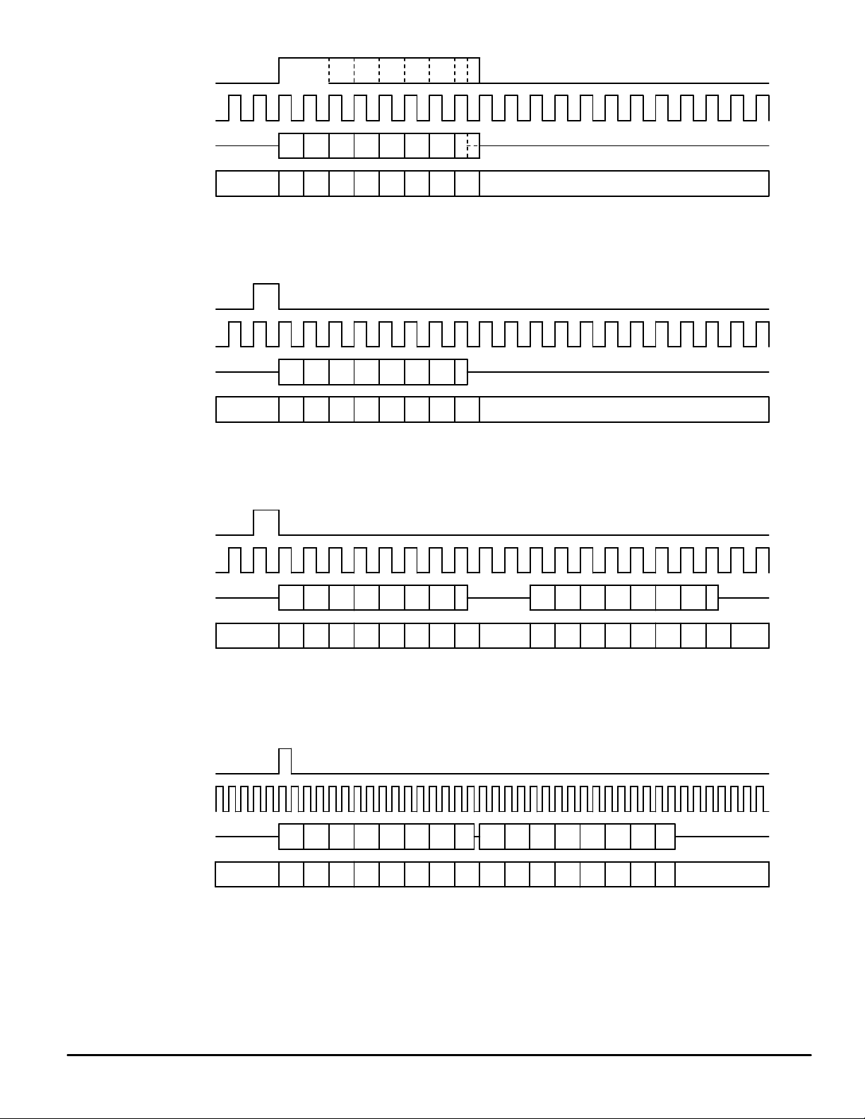
FST (FSR)
BCLKT (BCLKR)
DT
FST (FSR)
BCLKT (BCLKR)
DT
IDL SYNC (FST)
87654321
87654321DR DON’T CAREDON’T CARE
Figure 2a. Long Frame Sync (Transmit and Receive Have Individual Clocking)
87654321
8DR
7654321
DON’T CAREDON’T CARE
Figure 2b. Short Frame Sync (Transmit and Receive Have Individual Clocking)
IDL CLOCK (BCLKT)
IDL TX (DT)
IDL RX (DR)
Figure 2c. IDL Interface — BCLKR = 1 (Transmit and Receive Have Common Clocking)
FSC (FST)
DCL (BCLKT)
D
(DT)
out
Din (DR)
Figure 2d. GCI Interface — BCLKR = 0 (Transmit and Receive Have Common Clocking)
DON’T CARE
DON’T
CARE
Figure 2. Digital Timing Modes for the PCM Data Interface
87654321
DON’T
8
7654321 8
CARE
B2–CHANNEL (FSR = 1)B1–CHANNEL (FSR = 0)
87654321
87654321
B2–CHANNEL (FSR = 1)B1–CHANNEL (FSR = 0)
87654321
87654321
87654321
7654321
DON’T CARE
DON’T
CARE
MC14LC5480 MOTOROLA
6

Long Frame Sync
Long Frame Sync is the industry name for one type of
clocking format that controls the transfer of the PCM data
words. (Refer to Figure 2a.) The ‘‘Frame Sync’’ or ‘‘Enable’’ is
used for two specific synchronizing functions. The first is to
synchronize the PCM data word transfer, and the second is
to control the internal analog–to–digital and digital–to–analog
conversions. The term ‘‘Sync’’ refers to the function of synchronizing the PCM data word onto or off of the multiplexed
serial PCM data bus, which is also known as a PCM highway. The term ‘‘Long’’ comes from the duration of the frame
sync measured in PCM data clock cycles. Long Frame Sync
timing occurs when the frame sync is used directly as the
PCM data output driver enable. This results in the PCM output going low impedance with the rising edge of the transmit
frame sync, and remaining low impedance for the duration of
the transmit frame sync.
The implementation of Long Frame Sync has maintained
compatibility and been optimized for external clocking simplicity . This optimization includes the PCM data output going
low impedance with the logical AND of the transmit frame
sync (FST) with the transmit data bit clock (BCLKT). The optimization also includes the PCM data output (DT) remaining
low impedance until the middle of the LSB (seven and a half
PCM data clock cycles) or until the FST pin is taken low,
whichever occurs last. This requires the frame sync to be
approximately rising edge aligned with the initiation of the
PCM data word transfer, but the frame sync does not have a
precise timing requirement for the end of the PCM data word
transfer. The device recognizes Long Frame Sync clocking
when the frame sync is held high for two consecutive falling
edges of the transmit data clock. The transmit logic decides
on each frame sync whether it should interpret the next
frame sync pulse as a Long or a Short Frame Sync. This decision is used for receive circuitry also. The device is designed to prevent PCM bus contention by not allowing the
PCM data output to go low impedance for at least two frame
sync cycles after power is applied or when coming out of the
powered down mode.
The receive side of the device is designed to accept the
same frame sync and data clock as the transmit side and to
be able to latch its own transmit PCM data word. Thus the
PCM digital switch needs to be able to generate only one
type of frame sync for use by both transmit and receive sections of the device.
The logical AND of the receive frame sync with the receive
data clock tells the device to start latching the 8–bit serial
word into the receive data input on the falling edges of the
receive data clock. The internal receive logic counts the receive data clock cycles and transfers the PCM data word to
the digital–to–analog converter sequencer on the ninth data
clock rising edge.
This device is compatible with four digital interface modes.
To ensure that this device does not reprogram itself for a different timing mode, the BCLKR pin must change logic state
no less than every 125 µs. The minimum PCM data bit clock
frequency of 64 kHz satisfies this requirement.
Short Frame Sync
Short Frame Sync is the industry name for the type of
clocking format that controls the transfer of the PCM data
words (refer to Figure 2b). The ‘‘Frame Sync’’ or ‘‘Enable’’ is
used for two specific synchronizing functions. The first is to
synchronize the PCM data word transfer, and the second is
to control the internal analog–to–digital and digital–to–analog
conversions. The term ‘‘Sync’’ refers to the function of synchronizing the PCM data word onto or off of the multiplexed
serial PCM data bus, which is also known as a PCM highway. The term ‘‘Short’’ comes from the duration of the frame
sync measured in PCM data clock cycles. Short Frame Sync
timing occurs when the frame sync is used as a ‘‘pre–synchronization’’ pulse that is used to tell the internal logic to
clock out the PCM data word under complete control of the
data clock. The Short Frame Sync is held high for one falling
data clock edge. The device outputs the PCM data word beginning with the following rising edge of the data clock. This
results in the PCM output going low impedance with the rising edge of the transmit data clock, and remaining low impedance until the middle of the LSB (seven and a half PCM
data clock cycles).
The device recognizes Short Frame Sync clocking when
the frame sync is held high for one and only one falling edge
of the transmit data clock. The transmit logic decides on each
frame sync whether it should interpret the next frame sync
pulse as a Long or a Short Frame Sync. This decision is used
for receive circuitry also. The device is designed to prevent
PCM bus contention by not allowing the PCM data output to
go low impedance for at least two frame sync cycles after
power is applied or when coming out of the powered down
mode.
The receive side of the device is designed to accept the
same frame sync and data clock as the transmit side and to
be able to latch its own transmit PCM data word. Thus the
PCM digital switch needs to be able to generate only one
type of frame sync for use by both transmit and receive sections of the device.
The falling edge of the receive data clock latching a high
logic level at the receive frame sync input tells the device to
start latching the 8–bit serial word into the receive data input
on the following eight falling edges of the receive data clock.
The internal receive logic counts the receive data clock
cycles and transfers the PCM data word to the digital–to–
analog converter sequencer on the rising data clock edge after the LSB has been latched into the device.
This device is compatible with four digital interface modes.
To ensure that this device does not reprogram itself for a different timing mode, the BCLKR pin must change logic state
no less than every 125 µs. The minimum PCM data bit clock
frequency of 64 kHz satisfies this requirement.
Interchip Digital Link (IDL)
The Interchip Digital Link (IDL) Interface is one of two
standard synchronous 2B+D ISDN timing interface modes
with which this device is compatible. In the IDL mode, the device can communicate in either of the two 64 kbps B channels (refer to Figure 2c for sample timing). The IDL mode is
selected when the BCLKR pin is held high for two or more
FST (IDL SYNC) rising edges. The digital pins that control
the transmit and receive PCM word transfers are reprogrammed to accommodate this mode. The pins affected are
FST , FSR, BCLKT, DT, and DR. The IDL Interface consists of
four pins: IDL SYNC (FST), IDL CLK (BCLKT), IDL TX (DT),
and IDL RX (DR). The IDL interface mode provides access to
both the transmit and receive PCM data words with common
control clocks of IDL Sync and IDL Clock. In this mode, the
MC14LC5480MOTOROLA
7

FSR pin controls whether the B1 channel or the B2 channel
is used for both transmit and receive PCM data word transfers. When the FSR pin is low, the transmit and receive PCM
words are transferred in the B1 channel, and for FSR high
the B2 channel is selected. The start of the B2 channel is ten
IDL CLK cycles after the start of the B1 channel.
The IDL SYNC (FST, Pin 14) is the input for the IDL frame
synchronization signal. The signal at this pin is nominally
high for one cycle of the IDL Clock signal and is rising edge
aligned with the IDL Clock signal. (Refer to Figure 4 and the
IDL Timing specifications for more details.) This event identifies the beginning of the IDL frame. The frequency of the IDL
Sync signal is 8 kHz. The rising edge of the IDL SYNC (FST)
should be aligned approximately with the rising edge of
MCLK. MCLK must be one of the clock frequencies specified
in the Digital Switching Characteristics table, and is typically
tied to IDL CLK (BCLKT).
The IDL CLK (BCLKT, Pin 12) is the input for the PCM
data clock. All IDL PCM transfers and data control sequencing are controlled by this clock following the IDL SYNC. This
pin accepts an IDL data clock frequency of 256 kHz to 4.096
MHz.
The IDL TX (DT , Pin 13) is the output for the transmit PCM
data word. Data bits are output for the B1 channel on sequential rising edges of the IDL CLK signal beginning after
the IDL SYNC pulse. If the B2 channel is selected, then the
PCM word transfer starts on the eleventh IDL CLK rising
edge after the IDL SYNC pulse. The IDL TX pin will remain
low impedance for the duration of the PCM word until the
LSB after the falling edge of IDL CLK. The IDL TX pin will remain in a high impedance state when not outputting PCM
data or when a valid IDL Sync signal is missing.
The IDL RX (DR, Pin 8) is the input for the receive PCM
data word. Data bits are input for the B1 channel on sequential falling edges of the IDL CLK signal beginning after the
IDL SYNC pulse. If the B2 channel is selected, then the PCM
word is latched in starting on the eleventh IDL CLK falling
edge after the IDL SYNC pulse.
General Circuit Interface (GCI)
The General Circuit Interface (GCI) is the second of two
standard synchronous 2B+D ISDN timing interface modes
with which this device is compatible. In the GCI mode, the
device can communicate in either of the two 64 kbps B–
channels. (Refer to Figure 2d for sample timing.) The GCI
mode is selected when the BCLKR pin is held low for two or
more FST (FSC) rising edges. The digital pins that control
the transmit and receive PCM word transfers are reprogrammed to accommodate this mode. The pins affected are
FST, FSR, BCLKT, DT, and DR. The GCI Interface consists
of four pins: FSC (FST), DCL (BCLKT), D
(DR). The GCI interface mode provides access to both the
transmit and receive PCM data words with common control
clocks of FSC (frame synchronization clock) and DCL (data
clock). In this mode, the FSR pin controls whether the B1
channel or the B2 channel is used for both transmit and receive PCM data word transfers. When the FSR pin is low, the
transmit and receive PCM words are transferred in the B1
channel, and for FSR high the B2 channel is selected. The
start of the B2 channel is 16 DCL cycles after the start of the
B1 channel.
The FSC (FST, Pin 14) is the input for the GCI frame synchronization signal. The signal at this pin is nominally rising
(DT), and D
out
edge aligned with the DCL clock signal. (Refer to Figure 6
and the GCI Timing specifications for more details.) This
event identifies the beginning of the GCI frame. The frequency of the FSC synchronization signal is 8 kHz. The rising
edge of the FSC (FST) should be aligned approximately with
the rising edge of MCLK. MCLK must be one of the clock frequencies specified in the Digital Switching Characteristics
table, and is typically tied to DCL (BCLKT).
The DCL (BCLKT, Pin 12) is the input for the clock that
controls the PCM data transfers. The clock applied at the
DCL input is twice the actual PCM data rate. The GCI frame
begins with the logical AND of the FSC with the DCL. This
event initiates the PCM data word transfers for both transmit
and receive. This pin accepts a GCI data clock frequency of
512 kHz to 6.176 MHz for PCM data rates of 256 kHz to
3.088 MHz.
The GCI D
PCM data word. Data bits are output for the B1 channel on
alternate rising edges of the DCL clock signal, beginning with
the FSC pulse. If the B2 channel is selected, then the PCM
word transfer starts on the seventeenth DCL rising edge after
the FSC rising edge. The D
for 15–1/2 DCL clock cycles. The D
impedance after the second falling edge of the DCL clock
during the LSB of the PCM word. The D
a high–impedance state when not outputting PCM data or
when a valid FSC signal is missing.
The Din (DR, Pin 8) is the input for the receive PCM data
word. Data bits are latched in for the B1 channel on alternate
rising edges of the DCL clock signal, beginning with the second DCL clock after the rising edge of the FSC pulse. If the
B2 channel is selected then the PCM word is latched in starting on the eighteenth DCL rising edge after the FSC rising
edge.
(DT, Pin 13) is the output for the transmit
out
pin will remain low impedance
out
pin becomes high
out
pin will remain in
out
PRINTED CIRCUIT BOARD LAYOUT
CONSIDERATIONS
The MC14LC5480 is manufactured using high–speed
CMOS VLSI technology to implement the complex analog
signal processing functions of a PCM Codec–Filter. The fully–differential analog circuit design techniques used for this
device result in superior performance for the switched capacitor filters, the analog–to–digital converter (ADC) and the digital–to–analog converter (DAC). Special attention was given
to the design of this device to reduce the sensitivities of
noise, including power supply rejection and susceptibility to
radio frequency noise. This special attention to design includes a fifth order low–pass filter, followed by a third order
high–pass filter whose output is converted to a digital signal
in
with greater than 75 dB of dynamic range, all operating on a
single 5 V power supply. This results in a Mu–Law LSB size
for small audio signals of about 386 µV . The typical idle channel noise level of this device is less than one LSB. In addition
to the dynamic range of the codec–filter function of this device, the input gain–setting op amp has the capability of
greater than 35 dB of gain intended for an electret microphone interface.
This device was designed for ease of implementation, but
due to the large dynamic range and the noisy nature of the
environment for this device (digital switches, radio telephones, DSP front–end, etc.) special care must be taken to
assure optimum analog transmission performance.
MC14LC5480 MOTOROLA
8

PC BOARD MOUNTING
It is recommended that the device be soldered to the PC
board for optimum noise performance. If the device is to be
used in a socket, it should be placed in a low parasitic pin
inductance (generally , low–profile) socket.
POWER SUPPLY, GROUND, AND NOISE
CONSIDERATIONS
This device is intended to be used in switching applications which often require plugging the PC board into a rack
with power applied. This is known as ‘‘hot–rack insertion.’’ In
these applications care should be taken to limit the voltage
on any pin from going positive of the VDD pins, or negative of
the VSS pins. One method is to extend the ground and power
contacts of the PCB connector. The device has input protection on all pins and may source or sink a limited amount of
current without damage. Current limiting may be accomplished by series resistors between the signal pins and the
connector contacts.
The most important considerations for PCB layout deal
with noise. This includes noise on the power supply, noise
generated by the digital circuitry on the device, and cross
coupling digital or radio frequency signals into the audio signals of this device. The best way to prevent noise is to:
1. Keep digital signals as far away from audio signals as
possible.
2. Keep radio frequency signals as far away from the audio
signals as possible.
3. Use short, low inductance traces for the audio circuitry
to reduce inductive, capacitive, and radio frequency
noise sensitivities.
4. Use short, low inductance traces for digital and RF
circuitry to reduce inductive, capacitive, and radio
frequency radiated noise.
5. Bypass capacitors should be connected from the V
and VAG pins to VSS with minimal trace length. Ceramic
monolithic capacitors of about 0.1 µF are acceptable to
decouple the device from its own noise. The V
capacitor helps supply the instantaneous currents of the
digital circuitry in addition to decoupling the noise which
may be generated by other sections of the device or
other circuitry on the power supply. The VAG decoupling
capacitor helps to reduce the impedance of the VAG pin
to VSS at frequencies above the bandwidth of the V
generator, which reduces the susceptibility to RF noise.
6. Use a short, wide, low inductance trace to connect the
VSS ground pin to the power supply ground. The VSS pin
is the digital ground and the most negative power supply
pin for the analog circuitry . All analog signal processing
is referenced to the VAG pin, but because digital and RF
circuitry will probably be powered by this same ground,
care must be taken to minimize high frequency noise in
the VSS trace. Depending on the application, a double–
sided PCB with a VSS ground plane connecting all of the
digital and analog VSS pins together would be a good
grounding method. A multilayer PC board with a ground
plane connecting all of the digital and analog VSS pins
together would be the optimal ground configuration.
These methods will result in the lowest resistance and
the lowest inductance in the ground circuit. This is
important to reduce voltage spikes in the ground circuit
DD
DD
AG
resulting from the high speed digital current spikes. The
magnitude of digitally induced voltage spikes may be
hundreds of times larger than the analog signal the
device is required to digitize.
7. Use a short, wide, low inductance trace to connect the
VDD power supply pin to the 5 V power supply.
Depending on the application, a double–sided PCB with
VDD bypass capacitors to the VSS ground plane, as
described above, may complete the low impedance
coupling for the power supply . For a multilayer PC board
with a power plane, connecting all of the VDD pins to the
power plane would be the optimal power distribution
method. The integrated circuit layout and packaging
considerations for the 5 V VDD power circuit are
essentially the same as for the VSS ground circuit.
8. T he VAG pin is the reference for all analog signal
processing. In some applications the audio signal to be
digitized may be referenced to the VSS ground. To
reduce the susceptibility to noise at the input of the ADC
section, the three–terminal op amp may be used in a
differential to single–ended circuit to provide level
conversion from the VSS ground to the VAG ground with
noise cancellation. The op amp may be used for more
than 35 dB of gain in microphone interface circuits, which
will require a compact layout with minimum trace lengths
as well as isolation from noise sources. It is recommended that the layout be as symmetrical as possible to
avoid any imbalances which would reduce the noise
cancelling benefits of this differential op amp circuit.
Refer to the application schematics for examples of this
circuitry.
If possible, reference audio signals to the VAG pin
instead of to the VSS pin. Handset receivers and telephone line interface circuits using transformers may be
audio signal referenced completely to the VAG pin. Refer to the application schematics for examples of this
circuitry. The VAG pin cannot be used for ESD or line
protection.
9. For applications using multiple MC14LC5480 PCM
Codec–Filters, the VAG pins cannot be tied together. The
VAG pins are capable of sourcing and sinking current and
will each be driving the node, which will result in large
contention currents, crosstalk susceptibilities, and increased noise.
10. The MC14LC5480 is fabricated with advanced high–
speed CMOS technology that is capable of responding
to noise pulses on the clock pins of 1 ns or less. It should
be noted that noise pulses of such short duration may not
be seen with oscilloscopes that have less bandwidth
than 600 MHz. The most often encountered sources of
clock noise spikes are inductive or capacitive coupling of
high–speed logic signals, and ground bounce. The best
solution for addressing clock spikes from coupling is to
separate the traces and use short low inductance PC
board traces. To address ground bounce problems, all
integrated circuits should have high frequency bypass
capacitors directly across their power supply pins, with
low inductance traces for ground and power supply. A
less than optimum solution may be to limit the bandwidth
of the trace by adding series resistance and/or capacitance at the input pin.
MC14LC5480MOTOROLA
9
MAXIMUM RATINGS (Voltages Referenced to V
Rating Symbol Value Unit
DC Supply Voltage V
Voltage on Any Analog Input or Output Pin VSS – 0.3 to VDD + 0.3 V
Voltage on Any Digital Input or Output Pin VSS – 0.3 to VDD + 0.3 V
Operating Temperature Range T
Storage Temperature Range T
SS
Pin)
DD
stg
– 0.5 to 6 V
A
– 40 to + 85 °C
– 85 to +150 °C
POWER SUPPLY (T
DC Supply Voltage 4.75 5.0 5.25 V
Active Power Dissipation (VDD = 5 V) (No Load, PI ≥ VDD – 0.5 V)
Power–Down Dissipation (VIH for Logic Levels Must be ≥ 3.0 V) PDI = V
DIGITAL LEVELS (V
Input Low Voltage V
Input High Voltage V
Output Low Voltage (DT Pin, IOL= 2.5 mA) V
Output High Voltage (DT Pin, IOH = – 2.5 mA) V
Input Low Current (VSS ≤ Vin ≤ VDD) I
Input High Current (VSS ≤ Vin ≤ VDD) I
Output Current in High Impedance State (VSS ≤ DT ≤ VDD) I
Input Capacitance of Digital Pins (Except DT) C
Input Capacitance of DT Pin when High–Z C
NOTE: Bold type indicates a change from the MC145480 to the MC14LC5480.
= – 40 to + 85°C)
A
Characteristics
(No Load, PI ≤ VDD – 1.5 V)
FST and FSR = VSS, PDI
= + 5 V ± 5%, VSS = 0 V, TA = – 40 to + 85°C)
DD
Characteristics
= V
SS
DD
Min Typ Max Unit
—
—
—
—
Symbol Min Max Unit
IL
IH
OL
OH
IL
IH
OZ
in
out
15
15
0.01
0.05
— 0.6 V
2.4 — V
— 0.4 V
VDD – 0.5 — V
– 10 + 10 µA
– 10 + 10 µA
– 10 + 10 µA
— 10 pF
— 15 pF
24
25
0.5
1.0
mW
mW
MC14LC5480 MOTOROLA
10
ANALOG ELECTRICAL CHARACTERISTICS (V
Characteristics
Input Current TI+, TI– — ± 0.1 ± 1.0 µA
Input Resistance to VAG (VAG – 0.5 V ≤ Vin ≤ VAG + 0.5 V)
Input Capacitance TI+, TI– — — 10 pF
Input Offset V oltage of TG Op Amp TI+, TI– — — ± 5 mV
Input Common Mode Voltage Range TI+, TI– 1.2 VDD – 2.0 V
Input Common Mode Rejection Ratio TI+, TI– — 60 — dB
Gain Bandwidth Product (10 kHz) of TG Op Amp (RL ≥ 10 kΩ) — 3000 — kHz
DC Open Loop Gain of TG Op Amp (RL ≥ 10 kΩ) — 95 — dB
Equivalent Input Noise (C–Message) Between TI+ and TI– at TG — –30 — dBrnC
Output Load Capacitance for TG Op Amp 0 — 100 pF
Output Voltage Range for TG
(RL = 10 kΩ to VAG)
(RL = 2 kΩ to VAG)
Output Current (0.5 V ≤ V
Output Load Resistance to V
Output Impedance (0 to 3.4 kHz) RO+ or RO– — 1 — Ω
Output Load Capacitance RO+ or RO– 0 — 500 pF
DC Output Offset Voltage of RO+ or RO– Referenced to V
VAG Output Voltage Referenced to VSS (No Load) 2.2 2.4 2.6 V
VAG Output Current with ± 25 mV Change in Output Voltage ± 2.0 ± 10 — mA
Power Supply Rejection Ratio Transmit
(0 to 100 kHz @100 mVrms Applied to VDD, Receive
C–Message Weighting, All Analog Signals
Referenced to VAG Pin)
Input Current (VAG – 0.5 V ≤ PI ≤ VAG + 0.5 V) PI — ± 0.05 ± 1.0 µA
Input Resistance (VAG – 0.5 V ≤ PI ≤ VAG + 0.5 V) PI 10 — — MΩ
Input Offset Voltage PI — — ± 20 mV
Output Offset Voltage of PO+ Relative to PO– (Inverted Unity Gain for PO–) — — ± 50 mV
Output Current (VSS + 0.7 V ≤ PO+ or PO– ≤ VDD – 0.7 V) ± 10 — — mA
PO+ or PO– Output Resistance (Inverted Unity Gain for PO–) — 1 — Ω
Gain Bandwidth Product (10 kHz, Open Loop for PO–) — 1000 — kHz
Load Capacitance (PO+ or PO– to VAG, or PO+ to PO–) 0 — 1000 pF
Gain of PO+ Relative to PO– (RL = 300 Ω, + 3 dBm0, 1 kHz) – 0.2 0 + 0.2 dB
Total Signal to Distortion at PO+ and PO– with a 300 Ω Differential Load 45 60 — dBC
Power Supply Rejection Ratio 0 to 4 kHz
(0 to 25 kHz @ 100 mVrms Applied to VDD. 4 to 25 kHz
PO– Connected to PI. Differential or Measured
Referenced to VAG Pin.)
≤ VDD – 0.5 V) TG, RO+, RO– ± 1.0 — — mA
out
AG
= + 5 V ± 5%, VSS = 0 V, TA = – 40 to + 85°C)
DD
Min Typ Max Unit
TI+, TI–
TG, RO+, and RO– 2 — — kΩ
AG
Power Drivers PI, PO+, PO–
10 —
0.5
1.0
— — ± 25 mV
50
50
40
—
—
—
80
75
55
40
— MΩ
VDD – 0.5
VDD – 1.0
—
—
—
—
V
dBC
dB
NOTE: Bold type indicates a change from the MC145480 to the MC14LC5480.
MC14LC5480MOTOROLA
11
ANALOG TRANSMISSION PERFORMANCE
(VDD = + 5 V ± 5%, VSS = 0 V, All Analog Signals Referenced to VAG, 0 dBm0 = 0.775 Vrms = + 0 dBm @ 600 Ω, FST = FSR = 8 kHz,
BCLKT = MCLK = 2.048 MHz Synchronous Operation, TA = – 40 to + 85°C, Unless Otherwise Noted)
End–to–End A/D D/A
Characteristics
Absolute Gain (0 dBm0 @ 1.02 kHz, TA = 25°C, VDD = 5.0 V) — — – 0.25 + 0.25 – 0.25 + 0.25 dB
Absolute Gain Variation with Temperature
Absolute Gain Variation with Power Supply (TA = 25°C) — — — ± 0.03 — ±
Gain vs Level Tone (Mu–Law, Relative to – 10 dBm0, 1.02 kHz)
(Referenced to 25°C)
0 to + 70°C
– 40 to + 85°C——
+ 3 to – 40 dBm0
– 40 to – 50 dBm0
– 50 to – 55 dBm0
Gain vs Level Pseudo Noise, CCITT G.712 – 10 to – 40 dBm0
(A–Law, Relative to – 10 dBm0) – 40 to – 50 dBm0
Total Distortion, 1.02 kHz Tone (Mu–Law, C–Message Weighting)
– 50 to – 55 dBm0
+ 3 dBm0
0 to – 30 dBm0
– 40 dBm0
– 45 dBm0
Total Distortion, Pseudo Noise, CCITT G.714 (A–Law) – 3 dBm0
– 6 to – 27 dBm0
– 34 dBm0
– 40 dBm0
– 50 dBm0
– 55 dBm0
Idle Channel Noise (For End–to–End and A/D, See Note 1)
Frequency Response (Relative to 1.02 kHz @ 0 dBm0) 15 Hz
(Mu–Law, C–Message Weighted)
(A–Law, Psophometric W eighted)
50 Hz
60 Hz
200 Hz
300 to 3000 Hz
3000 to 3200 Hz
3300 Hz
3400 Hz
4600 Hz to 100 kHz
In–Band Spurious (1.02 kHz @ 0 dBm0, Transmit and Receive)
Out–of–Band Spurious at RO+ (300 to 3400 Hz @ 0 dBm0 in)
8400 to 100,000 Hz
Idle Channel Noise Selective (8 kHz, Input = VAG, 30 Hz Bandwidth) — – 70 — — — – 70 dBm0
Absolute Delay (1600 Hz) — — — 315 — 205 µs
Group Delay Referenced to 1600 Hz 500 to 600 Hz
Crosstalk of 1020 Hz @ 0 dBm0 from A/D or D/A (Note 2) — — — –75 —
Intermodulation Distortion of Two Frequencies of Amplitudes
(– 4 to – 21 dBm0 from the Range 300 to 3400 Hz)
NOTES:
1. Extrapolated from a 1020 Hz @ – 50 dBm0 distortion measurement to correct for encoder enhancement.
2. Selectively measured while stimulated with 2667 Hz @ – 50 dBm0.
3. Bold type indicates a change from the MC145480 to the MC14LC5480.
4000 Hz
3400
300 to
4600 to 7600 Hz
7600 to 8400 Hz
600 to 800 Hz
800 to 1000 Hz
1000 to 1600 Hz
1600 to 2600 Hz
2600 to 2800 Hz
2800 to 3000 Hz
Min Max Min Max Min Max
—
—
——± 0.03
± 0.05——
± 0.03
± 0.05
0.03
—
—
—
—
—
—
—
—
—
—
—
—
—
—
—
—
—
—
—
—
—
—
—
—
—
—
—
—
Hz — – 48 — – 48 — – 48
—
—
—
—
—
—
—
—
—
—
—
—
—
—
—
—
—
—
—
—
—
—
—
—
—
—
—
—
—
—
—
—
—
—
—
—
—
—
– 30
– 40
– 30
—
—
—
—
—
—
—
– 0.30
– 0.8
– 1.2
– 0.25
– 0.60
– 1.00
34
36
30
25
30
36
34
29
19
14
—
—
—
—
—
– 1.0
– 0.20
– 0.20
– 0.35
– 0.8
—
—
—
—
—
—
—
—
—
—
—
—
+ 0.20
+ 0.40
+ 0.80
+ 0.25
+ 0.30
+ 0.45
—
—
—
—
—
—
—
—
—
—
17
– 69
– 40
– 30
– 26
– 0.4
+ 0.15
+ 0.20
+ 0.15
0
– 14
– 32
—
—
—
210
130
70
35
70
95
145
– 0.20
– 0.40
– 0.80
– 0.25
– 0.30
– 0.45
34
36
30
25
30
36
35
30
20
15
—
—
– 0.5
– 0.5
– 0.5
– 0.5
– 0.15
– 0.20
– 0.35
– 0.85
—
—
—
—
—
– 40
– 40
– 40
– 30
—
—
—
+ 0.20
+ 0.40
+ 0.80
+ 0.25
+ 0.30
+ 0.45
– 79
+ 0.15
+ 0.20
+ 0.15
– 14
– 30
– 40
– 30
110
175
–75
— – 41 — – 41 — – 41
—
—
—
—
—
—
—
—
—
—
11
30
—
—
—
—
85
Units
dB
dB
dB
dB
dBC
dB
dBrnc0
dBm0p
0
0
0
0
0
dB
dB
dB
µs
dB
dB
MC14LC5480 MOTOROLA
12
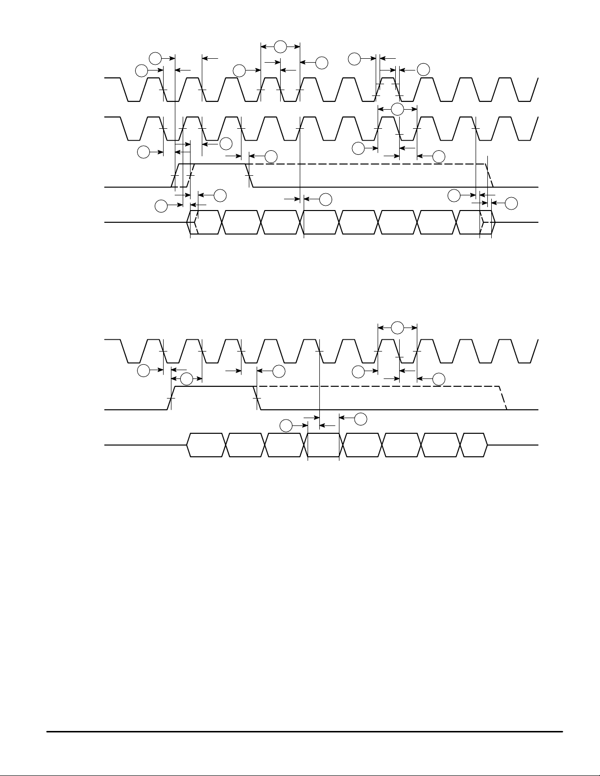
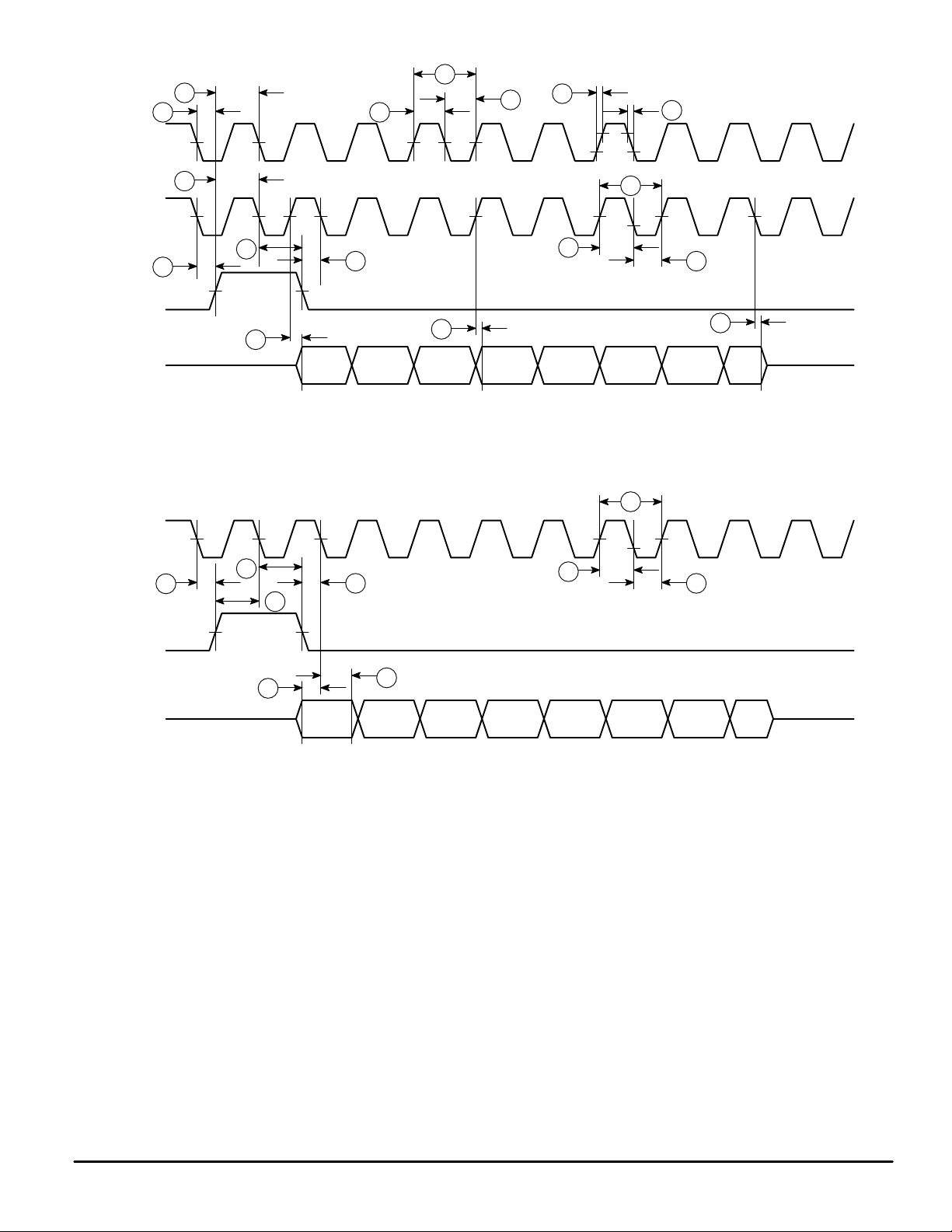
DIGITAL SWITCHING CHARACTERISTICS, LONG FRAME SYNC AND SHORT FRAME SYNC
(VDD = + 5 V ± 5%, VSS = 0 V, All Digital Signals Referenced to VSS, TA = – 40 to + 85°C, CL = 150 pF, Unless Otherwise Noted)
Ref.
No.
1 Master Clock Frequency for MCLK —
1 MCLK Duty Cycle for 256 kHz Operation 45 — 55 %
2 Minimum Pulse Width High for MCLK (Frequencies of 512 kHz or Greater) 50 — — ns
3 Minimum Pulse Width Low for MCLK (Frequencies of 512 kHz or Greater) 50 — — ns
4 Rise Time for All Digital Signals — — 50 ns
5 Fall Time for All Digital Signals — — 50 ns
6 Setup Time from MCLK Low to FST High 50 — — ns
7 Setup Time from FST High to MCLK Low 50 — — ns
8 Bit Clock Data Rate for BCLKT or BCLKR 64 — 4096 kHz
9 Minimum Pulse Width High for BCLKT or BCLKR 50 — — ns
10 Minimum Pulse Width Low for BCLKT or BCLKR 50 — — ns
11 Hold Time from BCLKT (BCLKR) Low to FST (FSR) High 20 — — ns
12 Setup Time for FST (FSR) High to BCLKT (BCLKR) Low 80 — — ns
13 Setup Time from DR Valid to BCLKR Low 0 — — ns
14 Hold Time from BCLKR Low to DR Invalid 50 — — ns
15 Hold Time from 2nd Period of BCLKT (BCLKR) Low to FST (FSR) Low 50 — — ns
16 Delay Time from FST or BCLKT, Whichever is Later, to DT for Valid MSB Data — — 60 ns
17 Delay Time from BCLKT High to DT for Valid Chord and Step Bit Data — — 60 ns
18 Delay Time from the Later of the 8th BCLKT Falling Edge, or the Falling Edge
of FST to DT Output High Impedance
19 Minimum Pulse Width Low for FST or FSR 50 — — ns
20 Hold Time from BCLKT (BCLKR) Low to FST (FSR) Low 50 — — ns
21 Setup Time from FST (FSR) Low to MSB Period of BCLKT (BCLKR) Low 50 — — ns
22 Delay Time from BCLKT High to DT Data Valid 10 — 60 ns
23 Delay Time from the 8th BCLKT Low to DT Output High Impedance 10 — 60 ns
Characteristics Min Typ Max Unit
LONG FRAME SPECIFIC TIMING
SHORT FRAME SPECIFIC TIMING
—
—
—
—
—
—
10 — 60 ns
256
512
1536
1544
2048
2560
4096
—
—
—
—
—
—
—
kHz
MC14LC5480MOTOROLA
13
MCLK
7
6 2
1
3
4
5
8
BCLKT
FST
DT
BCLKR
FSR
123456789
11
16
12
15
16
17
9
10
18
18
MSB CH1 CH2 CH3 ST1 ST2 ST3 LSB
8
123456789
11
12
15
9
10
DR
13
14
MSB CH1 CH2 CH3 ST1 ST2 ST3 LSB
Figure 3. Long Frame Sync Timing
MC14LC5480 MOTOROLA
14
7
6 2
MCLK
1
3
4
5
BCLKT
FST
DT
BCLKR
12
8
123456789
20
11
22
21
22
9
10
23
MSB CH1 CH2 CH3 ST1 ST2 ST3 LSB
8
123456789
11
20
12
21
9
10
FSR
DR
13
14
MSB CH1 CH2 CH3 ST1 ST2 ST3 LSB
Figure 4. Short Frame Sync Timing
MC14LC5480MOTOROLA
15
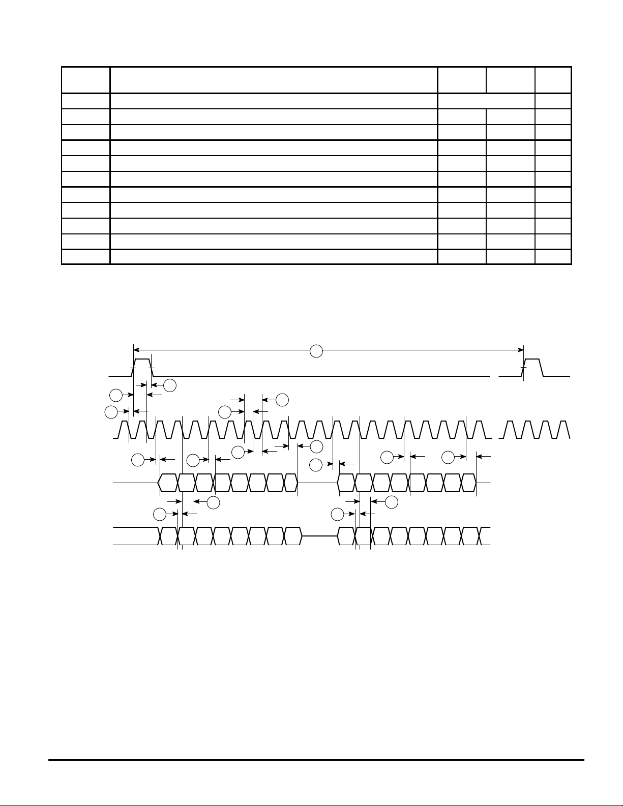
DIGITAL SWITCHING CHARACTERISTICS FOR IDL MODE
(VDD = 5.0 V ± 5%, TA = – 40 to + 85°C, CL = 150 pF, See Figure 5 and Note 1)
Ref.
No.
31 Time Between Successive IDL Syncs Note 2
32 Hold Time of IDL SYNC After Falling Edge of IDL CLK 20 — ns
33 Setup Time of IDL SYNC Before Falling Edge IDL CLK 60 — ns
34 IDL Clock Frequency 256 4096 kHz
35 IDL Clock Pulse Width High 50 — ns
36 IDL Clock Pulse Width Low 50 — ns
37 Data Valid on IDL RX Before Falling Edge of IDL CLK 20 — ns
38 Data Valid on IDL RX After Falling Edge of IDL CLK 75 — ns
39 Falling Edge of IDL CLK to High–Z on IDL TX 10 50 ns
40 Rising Edge of IDL CLK to Low–Z and Data Valid on IDL TX 10 60 ns
41 Rising Edge of IDL CLK to Data Valid on IDL TX — 50 ns
NOTES:
1. Measurements are made from the point at which the logic signal achieves the guaranteed minimum or maximum logic level.
2. In IDL mode, both transmit and receive 8–bit PCM words are accessed during the B1 channel, or both transmit and receive 8–bit PCM words
are accessed during the B2 channel as shown in Figure 5. IDL accesses must occur at a rate of 8 kHz (125 µs interval).
Characteristics Min Max Unit
IDLE SYNC
(FST)
IDL CLOCK
(BCLKT)
IDL TX
(DT)
IDL RX
(DR)
32
33
32
34
35
40
37 37
41
CH2
CH1MSB
36
38
LSBST3ST2ST1CH3CH2CH1MSB LSBST3ST2ST1CH3CH2CH1MSB
Figure 5. IDL Interface Timing
31
40
39
41 39
38
19181716151413121110987654321
LSBST3ST2ST1CH3CH2CH1MSBLSBST3ST2ST1CH3
21
MC14LC5480 MOTOROLA
16
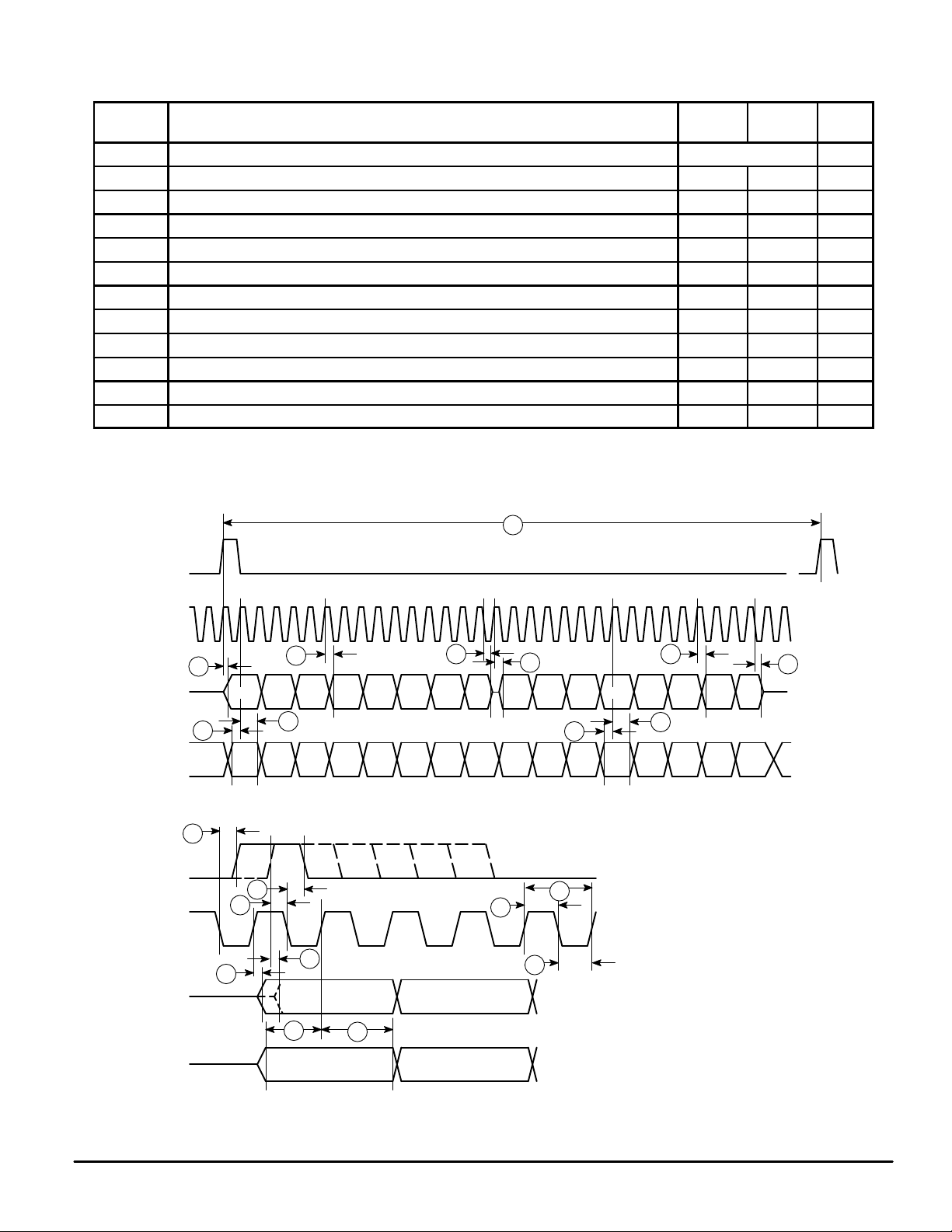
DIGITAL SWITCHING CHARACTERISTICS FOR GCI MODE
(VDD = 5.0 V ± 5%, TA = – 40 to + 85°C, CL = 150 pF, See Figure 6 and Note 1)
Ref.
No.
42 Time Between Successive FSC Pulses Note 2
43 DCL Clock Frequency 512 6176 kHz
44 DCL Clock Pulse Width High 50 — ns
45 DCL Clock Pulse Width Low 50 — ns
46 Hold Time of FSC After Falling Edge of DCL 20 — ns
47 Setup Time of FSC to DCL Falling Edge 60 — ns
48 Rising Edge of DCL (After Rising Edge of FSC) to Low Impedance and Valid Data of D
49 Rising Edge of FSC (While DCL is High) to Low Impedance and Valid Data of D
50 Rising Edge of DCL to Valid Data on D
51 Second DCL Falling Edge During LSB to High Impedance of D
52 Setup Time of Din Before Rising Edge of DCL 20 — ns
53 Hold Time of Din After DCL Rising Edge — 60 ns
NOTES:
1. Measurements are made from the point at which the logic signal achieves the guaranteed minimum or maximum logic level.
2. In GCI mode, both transmit and receive 8–bit PCM words are accessed during the B1 channel, or both transmit and receive 8–bit PCM words
are accessed during the B2 channel as shown in Figure 6. GCI accesses must occur at a rate of 8 kHz (125 µs interval).
Characteristics Min Max Unit
out
out
out
out
— 60 ns
— 60 ns
— 60 ns
10 50 ns
FSC
(FST)
DCL
(BCLKT)
D
(DT)
out
Din (DR)
FSC
(FST)
DCL
(BCLKT)
D
(DT)
out
46
49
52
1 343332302928272625242322212019181715 1614138765432
48
MSB
47
46
53
50
49
42
1211109
51
LSBST3ST2ST1CH3CH2CH1
LSBST3ST2ST1CH3CH2CH1MSB LSBST3ST2ST1CH3CH2CH1MSB
4321
48
52
43
44
5
45
50
53
31
51
LSBST3ST2ST1CH3CH2CH1MSB
CH1MSB
Din (DR)
52
53
CH1MSB
Figure 6. GCI Interface Timing
MC14LC5480MOTOROLA
17
AUDIO OUT
+ 5 V
0.1 µF
0.1
µ
10 k
10 k
F
Ω
Ω
1.0 µF
1.0 µF
8 kHz
PCM OUT
2.048 MHz
PCM IN
ANALOG IN
Y
+
–
1
2
3
4
5
6
7
8
9
RO+
RO–
PI
PO–
PO+
V
DD
FSR
DR
BCLKR
PDI
V
AG
TI+
TI–
TG
Mu/A
V
SS
FST
DT
BCLKT
MCLK
20
19
18
17
16
15
14
13
12
11 10
10 k
Ω
10 k
Ω
+ 5 V
Figure 7. MC14LC5480 Test Circuit with Differential Input and Output
AUDIO OUT
RL ≥ 2 k
Ω
AUDIO OUT
RL ≥ 150
Ω
10 k
1
RO+
2
3
4
5
6
7
8
9
RO–
PI
PO–
PO+
V
DD
FSR
DR
BCLKR
PDI
Ω
10 k
68
µ
F
10 k
+
Ω
+ 5 V
0.1 µF
Ω
V
AG
TI+
TI–
TG
Mu/A
V
SS
FST
DT
BCLKT
MCLK
20
19
18
17
16
15
14
13
12
11 10
10 k
Ω
+ 5 V
Figure 8. MC14LC5480 Test Circuit with Input and Output Referenced to V
10 k
µ
F
0.1
Ω
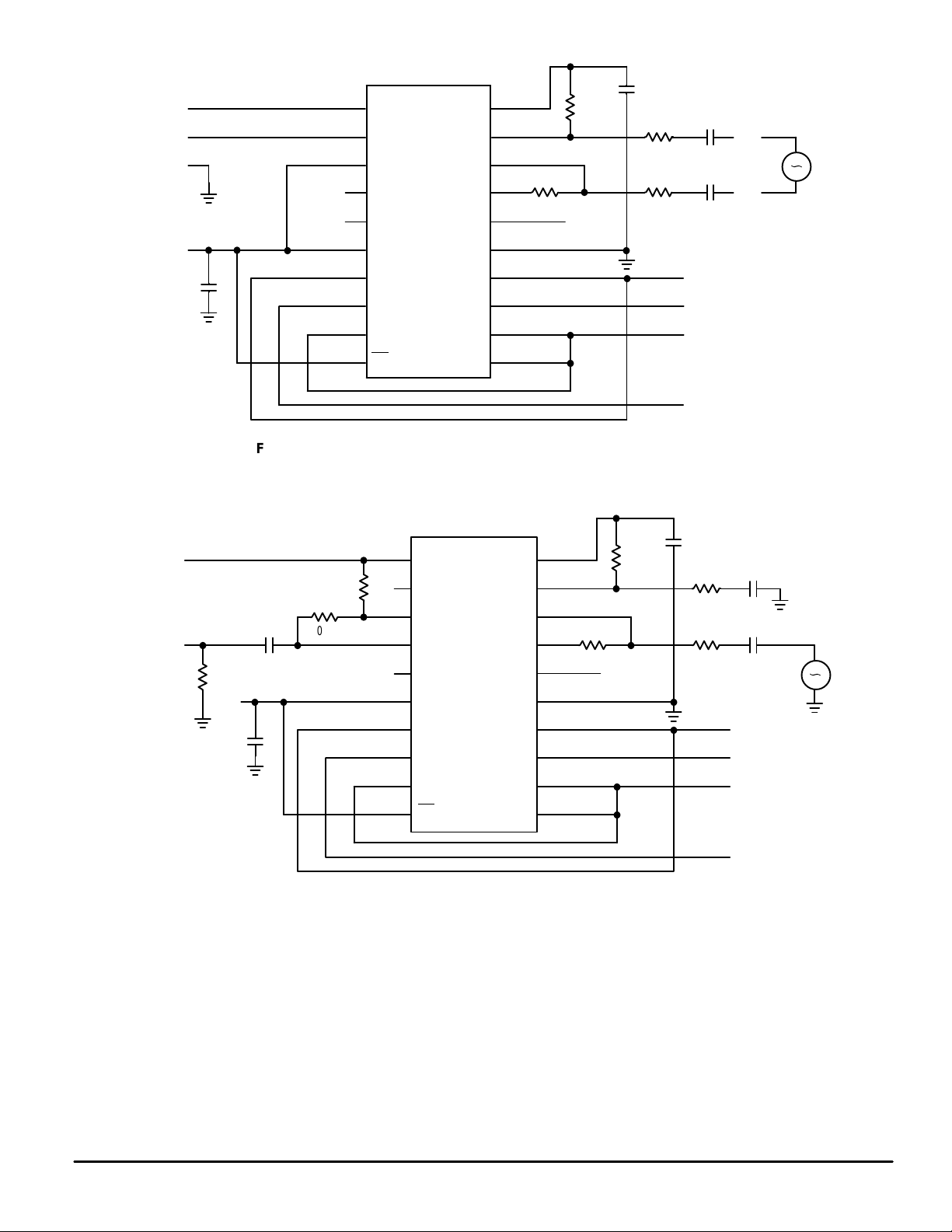
10 k
10 k
1.0 µF
Ω
Ω
ANALOG IN
1.0 µF
Y
8 kHz
PCM OUT
2.048 MHz
PCM IN
SS
MC14LC5480 MOTOROLA
18
+ 5 V
2.048 MHz
Ω
10 M
300
18 pF18 pF
Ω
2.048 MHz
(BCLKT, BCLKR, MCLK)
0.1
µ
F
8 kHz
2.048 MHz
V
CC
GND
V
J
1/2 MC74HC73
K
GND
256 8 97654321
R OSC
OSC IN
MC74HC4060
+ 5 V
CC
Q
Q
R
OSC
OUT 2
OUT 1
Q4Q8
R
Q
Q
+ 5 V
J
1/2 MC74HC73
K
Figure 9. Long Frame Sync Clock Circuit for 2.048 MHz
8 kHz
(FST, FSR)
REC
+ 5 V
0.1
+5 V
1 k
Ω
SIDETONE
68
µ
0.1 µF
420 pF
1
RO+
2
RO–
3
PI
4
PO–
5
PO+
6
V
DD
7
µ
F
+ 5 V
8
9
10
FSR
DR
BCLKR
PDI
V
AG
TI+
TI–
TG
Mu/A
V
SS
FST
DT
BCLKT
MCLK
20
19
18
17
16
15
14
13
12
11
+ 5 V
75 k
Ω
75 k
Ω
420 pF
F
0.1
µ
1 k
1 k
F
Ω
Ω
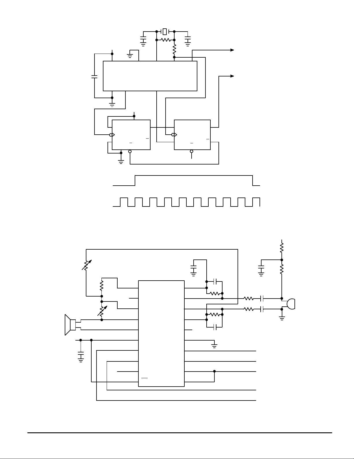
0.1 µF
IDL SYNC – 8 kHz
IDL TX
IDL CLOCK – 2.048 MHz
IDL RX
B1 – 0 V
B2 – + 5 V
1 k
Ω
MIC
Figure 10. MC14LC5480 Analog Interface to Handset with IDL Clocking
MC14LC5480MOTOROLA
19
1.0 µF
10 k
Ω
R0 = 600
1
RO+
2
10
3
4
5
6
7
8
9
RO–
PI
PO–
PO+
V
DD
FSR
DR
BCLKR
PDI
10 k
Ω
TIP
N = 1N = 1
RING
+ 5 V
0.1 µF
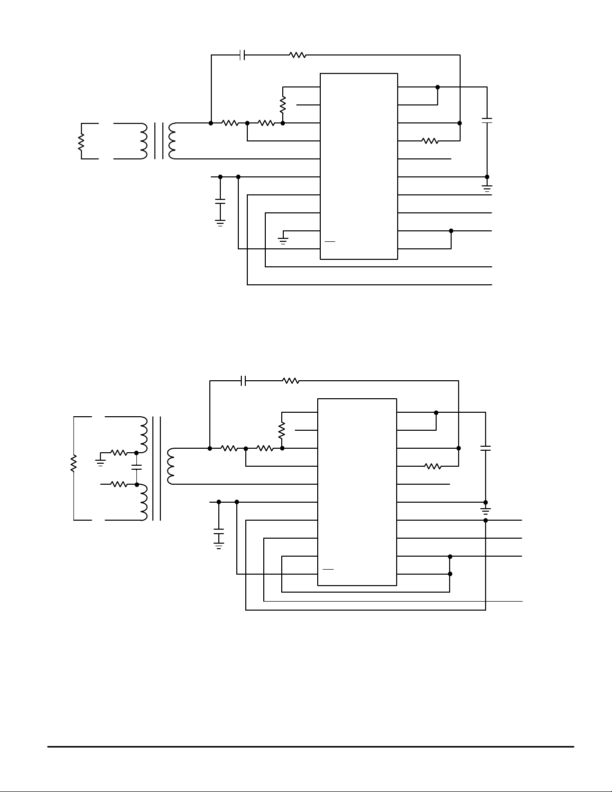
R0
10 k
Ω
Ω
V
AG
TI+
TI–
TG
Mu/A
V
SS
FST
DT
BCLKT
MCLK
20
19
18
17
16
15
14
13
12
11
10 k
Ω
Figure 11. MC14LC5480 Transformer Interface to 600 Ω Telephone Line with GCI Clocking
1.0
µ
F
10 k
Ω
+ 5 V
0.1 µF
FSC – 8 kHz
D
out
DCL – 4.096 MHz
D
in
B1 – 0 V
B2 – + 5 V
R0 = 600
– 48 V
Ω
TIP
N = 0.5
N = 0.5
RING
N = 0.5
+ 5 V
0.1 µF
1/4 R0
10 k
10 k
1
RO+
Ω
Ω
2
3
4
5
6
7
8
9
10
RO–
PI
PO–
PO+
V
DD
FSR
DR
BCLKR
PDI
V
AG
TI+
TI–
TG
Mu/A
V
SS
FST
DT
BCLKT
MCLK
20
19
18
17
16
15
14
13
12
11
20 k
Ω
0.1 µF
+ 5 V
8 kHz
PCM OUT
2.048 MHz
PCM IN
Figure 12. MC14LC5480 Step–Up Transformer Interface to 600 Ω Telephone Line
MC14LC5480 MOTOROLA
20
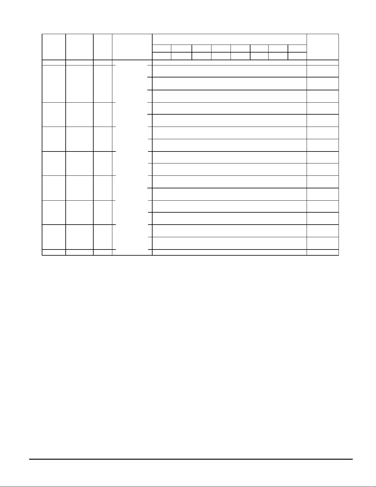
T able 3. Mu–Law Encode–Decode Characteristics
Normalized
Encode Normalized
Chord Number Step Decision Decode
Number of Steps Size Levels Sign Chord Chord Chord Step Step Step Step Levels
8159
8 16 256
7 16 128 2143
6 16 64 1055
51632511
4 16 16 239
3 16 8 103
2164 35
1152 3
11 11111111 0
NOTES:
1. Characteristics are symmetrical about analog zero with sign bit = 0 for negative analog values.
2. Digital code includes inversion of all magnitude bits.
7903
…
4319
4063
…
2015
…
991
…
479
…
223
…
95
…
31
…
1
0
12345678
1 0 0 0 0 0 0 0 8031
1 0 0 0 1 1 1 1 4191
1 0 0 1 1 1 1 1 2079
1 0 1 0 1 1 1 1 1023
1 0 1 1 1 1 1 1 495
1 1 0 0 1 1 1 1 231
11011111 99
11101111 33
11111110 2
Digital Code
…
…
…
…
…
…
…
…
…
…
…
…
…
…
…
…
MC14LC5480MOTOROLA
21
T able 4. A–Law Encode–Decode Characteristics
Normalized
Encode Normalized
Chord Number Step Decision Decode
Number of Steps Size Levels Sign Chord Chord Chord Step Step Step Step Levels
4096
7 16 128
6 16 64 1088
5 16 32 544
4 16 16 272
3 16 8 136
2164 68
1322 2
NOTES:
1. Characteristics are symmetrical about analog zero with sign bit = 0 for negative analog values.
2. Digital code includes inversion of all even numbered bits.
3968
…
2176
2048
…
1024
…
512
…
256
…
128
…
64
…
0
12345678
1 0 1 0 1 0 1 0 4032
1 0 1 0 0 1 0 1 2112
1 0 1 1 0 1 0 1 1056
1 0 0 0 0 1 0 1 528
1 0 0 1 0 1 0 1 264
1 1 1 0 0 1 0 1 132
11110101 66
11010101 1
Digital Code
…
…
…
…
…
…
…
…
…
…
…
…
…
…
MC14LC5480 MOTOROLA
22
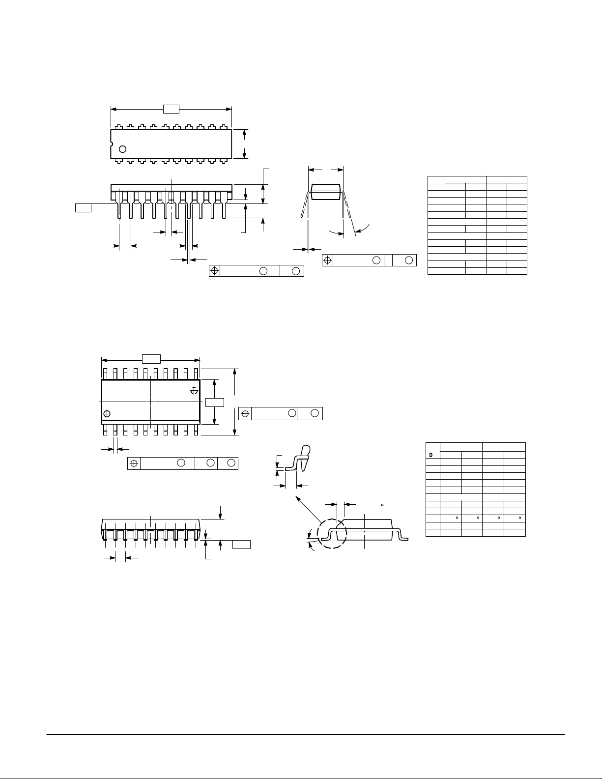
P ACKAGE DIMENSIONS
P SUFFIX
PLASTIC DIP
CASE 738–03
-T-
SEATING
PLANE
-A-
1120
B
110
C
K
E
N
GF
D
20 PL
0.25 (0.010) T A
M M
SOG PACKAGE
CASE 751D–04
–A–
20
11
–B–
P10X
0.010 (0.25)
1
10
D20X
0.010 (0.25) B
M
S
A
T
S
C
SEATING
–T–
18X
G
K
PLANE
DW SUFFIX
M
M
B
J
F
M
L
M
J 20 PL
0.25 (0.010) T B
R
X 45
M M
_
NOTES:
1. DIMENSIONING AND TOLERANCING PER ANSI
Y14.5M, 1982.
2. CONTROLLING DIMENSION: INCH.
3. DIMENSION L TO CENTER OF LEAD WHEN
FORMED PARALLEL.
4. DIMENSION B DOES NOT INCLUDE MOLD
FLASH.
INCHES MILLIMETERS
MIN MINMAX MAX
DIM
A
B
C
D
E
F
G
J
K
L
M
N
NOTES:
1. DIMENSIONING AND TOLERANCING PER
ANSI Y14.5M, 1982.
2. CONTROLLING DIMENSION: MILLIMETER.
3. DIMENSIONS A AND B DO NOT INCLUDE
MOLD PROTRUSION.
4. MAXIMUM MOLD PROTRUSION 0.150
(0.006) PER SIDE.
5. DIMENSION D DOES NOT INCLUDE
DAMBAR PROTRUSION. ALLOWABLE
DAMBAR PROTRUSION SHALL BE 0.13
(0.005) TOTAL IN EXCESS OF D DIMENSION
AT MAXIMUM MATERIAL CONDITION.
DIM MIN MAX MIN MAX
A 12.65 12.95 0.499 0.510
B 7.40 7.60 0.292 0.299
C 2.35 2.65 0.093 0.104
D 0.35 0.49 0.014 0.019
F 0.50 0.90 0.020 0.035
G 1.27 BSC 0.050 BSC
J 0.25 0.32 0.010 0.012
K 0.10 0.25 0.004 0.009
M 0 7 0 7
P 10.05 10.55 0.395 0.415
R 0.25 0.75 0.010 0.029
1.070
1.010
0.260
0.240
0.180
0.150
0.022
0.015
0.050 BSC
0.070
0.050
0.100 BSC
0.015
0.008
0.140
0.110
0.300 BSC
15°
°
0
0.040
0.020
__
25.66
27.17
6.10
6.60
3.81
4.57
0.39
0.55
1.27 BSC
1.27
1.77
2.54 BSC
0.21
0.38
2.80
3.55
7.62 BSC
°
0
15
1.01
0.51
INCHESMILLIMETERS
__
°
MC14LC5480MOTOROLA
23
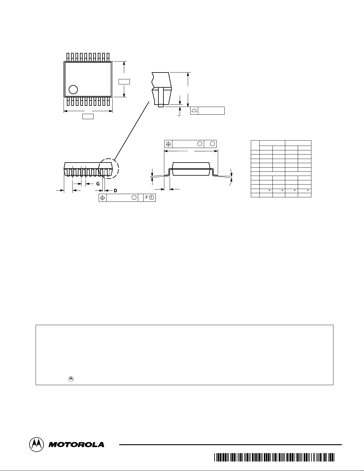
SD SUFFIX
SSOP
CASE 940C–02
20 11
A
–P–
G
H
B
–R–
101
D
0.120 (0.005) T
M
J
S
P
C
N
0.25 (0.010)
L
F
NOTE 4
0.076 (0.003)
M
M
R
NOTES:
1. CONTROLLING DIMENSION: MILLIMETER.
2. DIMENSIONS AND TOLERANCES PER ANSI
Y14.5M, 1982.
3. DIMENSIONS A AND B DO NOT INCLUDE
MOLD FLASH OR PROTRUSIONS AND ARE
MEASURED AT THE PARTING LINE. MOLD
FLASH OR PROTRUSIONS SHALL NOT
EXCEED 0.15MM PER SIDE.
4. DIMENSION IS THE LENGTH OF TERMINAL
FOR SOLDERING TO A SUBSTRATE.
5. TERMINAL POSITIONS ARE SHOWN FOR
REFERENCE ONLY.
6. THE LEAD WIDTH DIMENSION DOES NOT
INCLUDE DAMBAR PROTRUSION.
ALLOWABLE DAMBAR PROTRUSION SHALL
BE 0.08MM TOTAL IN EXCESS OF THE LEAD
WIDTH DIMENSION.
DIM MIN MAX MIN MAX
A 7.10 7.30 0.280 0.287
B 5.20 5.38 0.205 0.212
C 1.75 1.99 0.069 0.078
M
D 0.25 0.38 0.010 0.015
F 0.65 1.00 0.026 0.039
G 0.65 BSC 0.026 BSC
H 0.59 0.75 0.023 0.030
J 0.10 0.20 0.004 0.008
L 7.65 7.90 0.301 0.311
M 0 8 0 8
N 0.05 0.21 0.002 0.008
INCHESMILLIMETERS
____
Motorola reserves the right to make changes without further notice to any products herein. Motorola makes no warranty, representation or guarantee regarding
the suitability of its products for any particular purpose, nor does Motorola assume any liability arising out of the application or use of any product or circuit,
and specifically disclaims any and all liability, including without limitation consequential or incidental damages. “T ypical” parameters can and do vary in different
applications. All operating parameters, including “T ypicals” must be validated for each customer application by customer’s technical experts. Motorola does
not convey any license under its patent rights nor the rights of others. Motorola products are not designed, intended, or authorized for use as components in
systems intended for surgical implant into the body, or other applications intended to support or sustain life, or for any other application in which the failure of
the Motorola product could create a situation where personal injury or death may occur. Should Buyer purchase or use Motorola products for any such
unintended or unauthorized application, Buyer shall indemnify and hold Motorola and its officers, employees, subsidiaries, affiliates, and distributors harmless
against all claims, costs, damages, and expenses, and reasonable attorney fees arising out of, directly or indirectly, any claim of personal injury or death
associated with such unintended or unauthorized use, even if such claim alleges that Motorola was negligent regarding the design or manufacture of the part.
Motorola and are registered trademarks of Motorola, Inc. Motorola, Inc. is an Equal Opportunity/Affirmative Action Employer.
How to reach us:
USA/EUROPE: Motorola Literature Distribution; JAPAN: Nippon Motorola Ltd.; Tatsumi–SPD–JLDC, Toshikatsu Otsuki,
P.O. Box 20912; Phoenix, Arizona 85036. 1–800–441–2447 6F Seibu–Butsuryu–Center , 3–14–2 Tatsumi Koto–Ku, Tokyo 135, Japan. 03–3521–8315
MFAX: RMF AX0@email.sps.mot.com – T OUCHTONE (602) 244–6609 HONG KONG: Motorola Semiconductors H.K. Ltd.; 8B Tai Ping Industrial Park,
INTERNET: http://Design–NET .com 51 Ting Kok Road, Tai Po, N.T., Hong Kong. 852–26629298
MC14LC5480 MOTOROLA
24
◊
*MC14LC5480/D*
MC14LC5480/D
 Loading...