

Motorola MC145740F Datasheet
MC145740
MOTOROLA
1
Product Preview
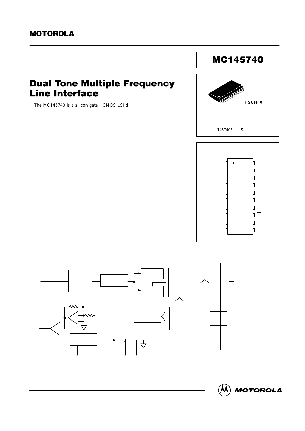
The MC145740 is a silicon gate HCMOS LSI designed for general purpose
Dual Tone Multiple Frequency (DTMF) communications, and contains a DTMF
signal generator and a receiver for all 16 standard digits.
The generator block has a differential line driver which drives a 600 Ω load
with 0 dBm level. The transmit signal level is adjusted in 1 dB steps by the
programmable attenuator.
The receiver block has an Auto Gain Control (AGC) amplifier to demodulate
50 dB (typ) dynamic range of DTMF signals to the hexadecimal codes.
The device also includes a serial control interface that permits a CPU to
exercise the following built–in features.
• Single Power Supply: 3.6 to 5.5 V
• DTMF Generator and Receiver for All 16 Standard Digits
• 0 dBm Line Driver Into 600 Ω Load
• AGC Amplifier
• Programmable Transmit Attenuator
• Serial Control Interface
• Power Down Mode, Less Than 1 µA
BLOCK DIAGRAM
+
–
RxA
DSI
TxA2
TxA1
Rx GAIN
CONTROL
WITH AGC
AMP
ANTI–ALIAS
FILTER
SMOOTHING
FILTER AND
Tx GAIN
CONTROL
CLOCK
GENERATOR
DTMF
GENERATOR
CONTROL REGISTER
AND
SERIAL INTERFACE
HIGH–BAND
BPF
LOW–BAND
BPF
DTMF
DETECTER
TIMING
CIRCUIT
AGC
out
FC1 FC2
X1 X2 VDDVSSV
ref
DV
TD
EN
CLK
DATA
R/W
– 1
This document contains information on a product under development. Motorola reserves the right to change or discontinue this product without notice.
Order this document
by MC145740/D
SEMICONDUCTOR TECHNICAL DATA
PIN ASSIGNMENT
F SUFFIX
SOG PACKAGE
CASE 751J
ORDERING INFORMATION
MC145740F SOG Package
FC1
AGC
out
RxA
TxA2
TxA1
V
SS
X2
X1
FC2
V
ref
5
4
3
2
1
10
9
8
7
6
14
15
16
17
18
19
20
11
12
13
EN
CLK
V
SS
V
DD
DSI
V
DD
DV
TD
R/W
DATA
20
1
Motorola, Inc. 1996
REV 0
8/96
MC145740
MOTOROLA
2
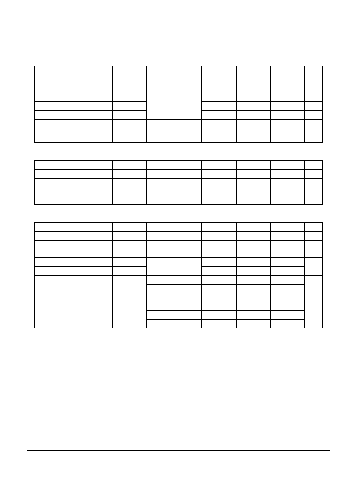
MAXIMUM RATINGS (Voltages Referenced to V
SS
Unless Otherwise Noted)
Ratings
Symbol
Value
Unit
DC Supply Voltage
V
CC
– 0.5 to + 7.0
V
Input Voltage, All Pins
V
in
– 0.5 to VCC + 0.5
V
DC Current Per Pin
I
± 20
mA
Power Dissipation
P
D
500
mW
Storage Temperature Range
T
stg
– 65 to + 150
°C
RECOMMENDED OPERATING CONDITIONS
Parameter Symbol Min Typ Max Unit
DC Supply Voltage V
CC
3.6 5 5.5 V
Input Voltage, All Pins V
in
0 — V
CC
V
Input Rise or Fall Time tr, t
f
0 — 500 ns
Crystal Frequency f
osc
— 3.5795 — MHz
Operating Temperature Range T
A
– 20 25 70 °C
DC ELECTRICAL CHARACTERISTICS (V
CC
= 5 V ± 10%, TA = – 20 to 70°C)
Parameter
Symbol Condition Min Typ Max Unit
Input Voltage H Level V
IH
3.15 — —
V
EN, CLK, DATA, R/W L Level V
IL
— — 1.1
Output Voltage H Level V
OH
IOH = 20 µA VCC – 0.1 VCC – 0.01 —
V
DV , TD, DATA L Level V
OL
IOL = – 20 µA
IOL = – 2 mA
—
—
0.01
—
0.1
0.4
Input Current R/W, DATA, EN, CLK I
in
Vin = VDD or V
SS
— ± 1.0 ± 10.0 µA
Supply Current I
DD
DTMF Tx Mode — 5 —
mA
DTMF Rx Mode — 8 —
Standby Current I
DD
Power Down 1 — — 500
µA
Power Down 2 — — 1
This device contains circuitry to protect the
inputs against damage due to high static voltages or electric fields. However, it is advised
that normal precautions be taken to avoid
applications of any voltage higher than maximum rated voltages to this high impedance
circuit. For proper operation, it is recommended
that Vin and V
out
be constrained to the range
VSS ≤ (Vin or V
out
) ≤ VDD.
Reliability of operation is enhanced if unused
logic inputs are tied to an appropriate logic voltage level (e.g., either VSS or VDD).
MC145740
MOTOROLA
3
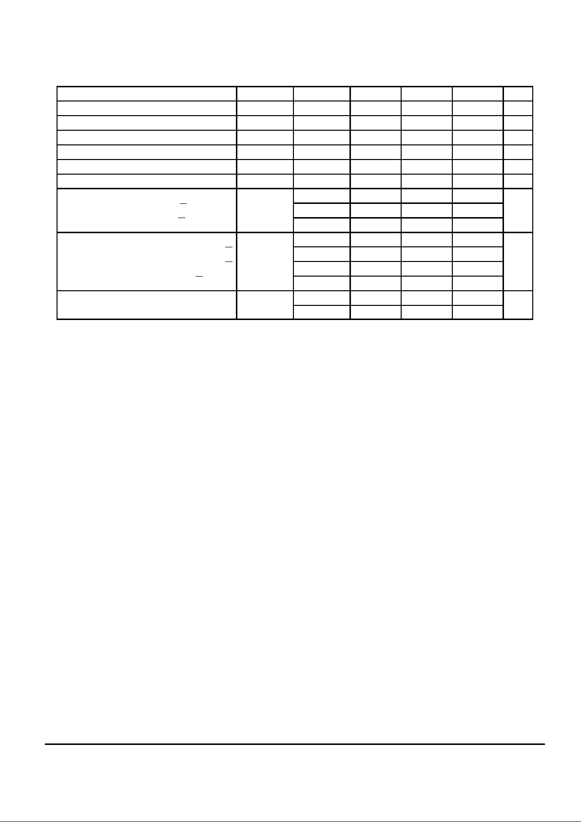
AC ELECTRICAL CHARACTERISTICS
DTMF TRANSMIT CHARACTERISTICS (V
CC
= 5 V ± 10%, TA = – 20 to 70°C)
Parameter Symbol Condition Min Typ Max Unit
Transmit Level Low Group V
fl
Attenuator = 0 dB
— 2.5 —
dBm
High Group V
fh
f
osc
= 3.579545 MHz
V
TxA1
– V
TxA2
— 3.5 —
High Group Pre–Emphasis PE
V
TxA1
V
TxA2
RL = 1.2 kΩ
0 — 3 dB
DTMF Distortion DIST — 5 — %
DTMF Frequency Variation ∆fV – 1 — 1 %
Out–of–Band Energy
(See Figure 1)
V
OE
— — —
Setup Time t
osc
— 4 — ms
TRANSMIT ATTENUATOR CHARACTERISTICS (V
CC
= 5 V ± 10%, TA = – 20 to 70°C)
Parameter
Symbol Condition Min Typ Max Unit
Attenuator Range ARNG 0 — 15 dB
Attenuator Accuracy AACC
1 dB – 5 dB – 0.5 — 0.5
dB
6 dB – 9 dB – 1 — 1
10 dB – 15 dB – 1.7 — 1
DTMF RECEIVER CHARACTERISTICS (V
CC
= 5 V ± 10%, TA = – 20 to 70°C)
Parameter
Symbol Condition Min Typ Max Unit
Input Impedance RIDTMF 50 — — kΩ
Detect Signal Level (Each Tone) – 48 — 0 dBm
Twist (High Group/Low Group) – 10 — 10 dB
Frequency Detect Band Width
See Figure 3
± 1.5% ± 2 Hz — —
% fc
Frequency Reject Band Width — — ± 3.5
DTMF Detect Timing OFF to ON
TVD
ON
CD1 = 0, CD0 = 1 — 20 —
ms
(See Figure 2)
CD1 = 1, CD0 = 0 — 30 —
CD1 = 1, CD0 = 1 — 40 —
ON to OFF TVD
OFF
CD1 = 0, CD0 = 1 — 20 —
CD1 = 1, CD0 = 0 — 30 —
CD1 = 1, CD0 = 1 — 20 —
MC145740
MOTOROLA
4
SWITCHING CHARACTERISTICS (V
CC
= 5 V ± 10%, TA = – 20 to 70°C, See Figure 4)
Parameter Symbol Number Min Typ Max Unit
Pulse Width (H) EN, SCK t
wh
1 50 — — ns
Pulse Width (L) EN, SCK t
wl
2 50 — — ns
Clock Cycle t
c
3 100 — — ns
Input Rise Time t
r
4 — — 2 µs
Input Fall Time t
f
5 — — 2 µs
Recovery Time EN to SCK t
rec
6, 18 50 — — ns
Setup Time DATA to SCK
t
su
7 50 — —
ns
R/W Low to DATA 9 100 — —
R/W High to DATA 12 50 — —
Hold Time SCK to DATA
t
h
8 50 — —
ns
EN to R/W 10 50 — —
DATA to R/W 14 50 — —
R/W to DATA 15 50 — —
Read Data Delay Time EN to DATA
t
d
13 — — 50
ns
SCK to DATA 17 — — 50
 Loading...