

MOTOROLA MC14572UBCP, MC14572UBD, MC14572UBDR2, MC14572UBF, MC14572UBFEL Datasheet
MC14572UB
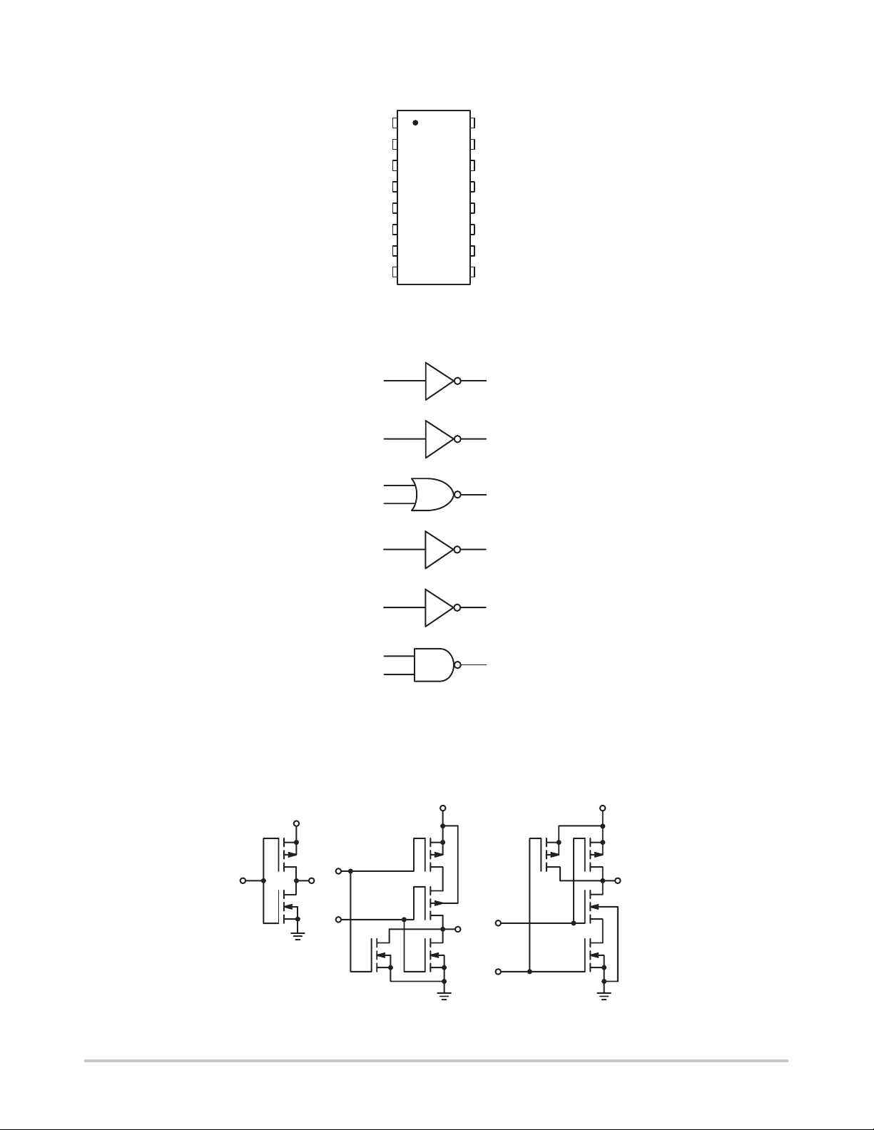
Hex Gate
The MC14572UB hex functional gate is constructed with MOS
P–channel and N–channel enhancement mode devices in a single
monolithic structure. These complementary MOS logic gates find
primary use where low power dissipation and/or high noise immunity
is desired. The chip contains four inverters, one NOR gate and one
NAND gate.
• Diode Protection on All Inputs
• Single Supply Operation
• Supply Voltage Range = 3.0 Vdc to 18 Vdc
• NOR Input Pin Adjacent to V
• NAND Input Pin Adjacent to V
Inverter
• NOR Output Pin Adjacent to Inverter Input Pin For OR Application
• NAND Output Pin Adjacent to Inverter Input Pin For AND
Application
• Capable of Driving T wo Low–power TTL Loads or One Low–Power
Schottky TTL Load over the Rated T emperature Range
MAXIMUM RATINGS (Voltages Referenced to V
Symbol
V
DD
Vin, V
Iin, I
P
T
T
stg
T
2. Maximum Ratings are those values beyond which damage to the device
may occur.
3. Temperature Derating:
Plastic “P and D/DW” Packages: – 7.0 mW/_C From 65_C To 125_C
This device contains protection circuitry to guard against damage due to high
static voltages or electric fields. However, precautions must be taken to avoid
applications of any voltage higher than maximum rated voltages to this
high–impedance circuit. For proper operation, Vin and V
to the range V
Unused inputs must always be tied to an appropriate logic voltage level (e.g.,
either V
DC Supply Voltage Range –0.5 to +18.0 V
Input or Output Voltage Range
out
Input or Output Current
out
Power Dissipation,
D
Ambient Temperature Range –55 to +125 °C
A
Storage Temperature Range –65 to +150 °C
Lead Temperature
L
SS
or VDD). Unused outputs must be left open.
SS
Parameter Value Unit
(DC or Transient)
(DC or Transient) per Pin
per Package (Note 3.)
(8–Second Soldering)
v (Vin or V
out
Pin to Simplify Use As An Inverter
SS
Pin to Simplify Use As An
DD
) (Note 2.)
SS
–0.5 to VDD + 0.5 V
±10 mA
500 mW
260 °C
should be constrained
) v VDD.
out
http://onsemi.com
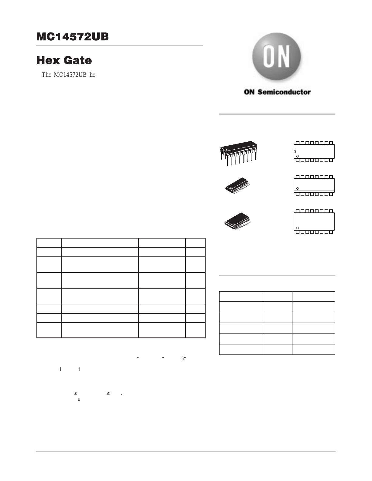
MARKING
DIAGRAMS
16
PDIP–16
P SUFFIX
CASE 648
SOIC–16
D SUFFIX
CASE 751B
SOEIAJ–16
F SUFFIX
CASE 966
A = Assembly Location
WL or L = Wafer Lot
YY or Y = Year
WW or W = Work Week
MC14572UBCP
AWLYYWW
1
16
14572U
AWLYWW
1
16
MC14572UB
AWLYWW
1
ORDERING INFORMATION
Device Package Shipping
MC14572UBCP PDIP–16 2000/Box
MC14572UBD SOIC–16 48/Rail
MC14572UBDR2 SOIC–16 2500/Tape & Reel
MC14572UBF SOEIAJ–16 See Note 1.
MC14572UBFEL SOEIAJ–16 See Note 1.
1. For ordering information on the EIAJ version of
the SOIC packages, please contact your local
ON Semiconductor representative.
Semiconductor Components Industries, LLC, 2000
March, 2000 – Rev . 3
1 Publication Order Number:
MC14572UB/D
MC14572UB
PIN ASSIGNMENT
OUT
1
A
IN
2
A
OUT
3
B
IN
4
B
OUT
C
IN 1
6
C
IN 2
7
C
V
8
SS
LOGIC DIAGRAM
V
16
DD
15
IN 2
F
IN 1
14
F
13
OUT
F
125
IN
E
OUT
11
10
E
IN
D
OUT
9
D
2
4
6
7
10
12
14
15
V
= PIN 16
DD
V
= PIN 8
SS
CIRCUIT SCHEMATIC
1
3
5
9
11
13
V
V
DD
7
2
1
6
V
SS
DD
14
5
V
DD
13
15
V
SS
V
SS
http://onsemi.com
2
MC14572UB
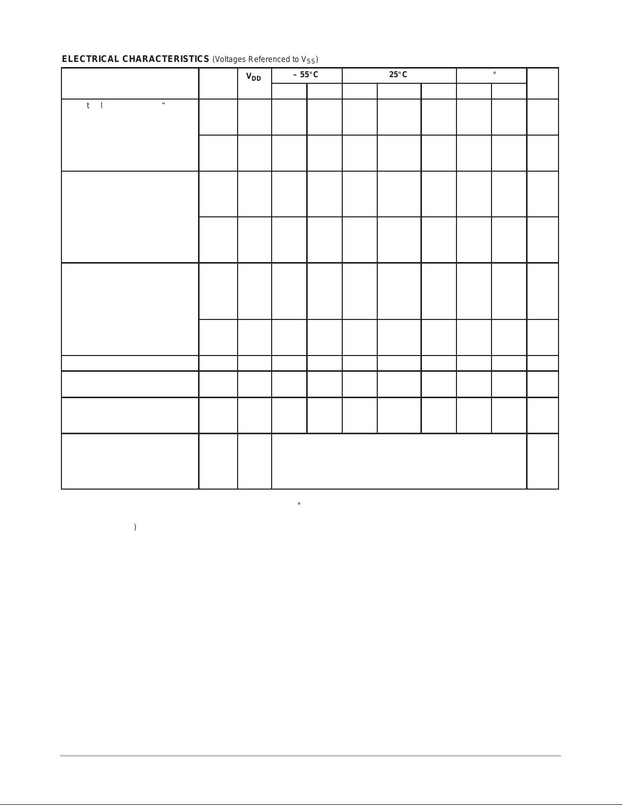
ELECTRICAL CHARACTERISTICS (Voltages Referenced to V
V
DD
Characteristic Symbol
Output Voltage “0” Level
V
= VDD or 0
in
Vin = 0 or V
DD
“1” Level V
Input Voltage “0” Level
(V
= 4.5 or 0.5 Vdc)
O
(V
= 9.0 or 1.0 Vdc)
O
(V
= 13.5 or 1.5 Vdc)
O
“1” Level
(V
= 0.5 or 4.5 Vdc)
O
= 1.0 or 9.0 Vdc)
(V
O
(V
= 1.5 or 13.5 Vdc)
O
Output Drive Current
(V
= 2.5 Vdc) Source
OH
(V
= 4.6 Vdc)
OH
(V
= 9.5 Vdc)
OH
(V
= 13.5 Vdc)
OH
(VOL = 0.4 Vdc) Sink
(V
= 0.5 Vdc)
OL
= 1.5 Vdc)
(V
OL
Input Current I
Input Capacitance
(V
= 0)
in
Quiescent Current
(Per Package)
Total Supply Current
(5.) (6.)
(Dynamic plus Quiescent,
Per Package)
= 50 pF on all outputs, all
(C
L
V
OL
OH
V
V
I
OH
I
OL
in
C
I
DD
I
Vdc
5.0
10
15
5.0
10
15
IL
5.0
10
15
IH
5.0
10
15
5.0
5.0
10
15
5.0
10
15
Min Max Min Typ
—
—
—
4.95
9.95
14.95
—
—
—
4.0
8.0
12.5
– 1.2
– 0.25
– 0.62
– 1.8
0.64
1.6
4.2
15 — ±0.1 — ±0.00001 ±0.1 — ±1.0 µAdc
in
T
— — — — 5.0 7.5 — — pF
5.0
10
15
—
—
—
5.0
10
15
)
SS
– 55_C 25_C 125_C
(4.)
Max Min Max
0.05
0.05
0.05
—
—
—
1.0
2.0
2.5
—
—
—
—
—
—
—
—
—
—
0.25
0.5
1.0
—
—
—
4.95
9.95
14.95
—
—
—
4.0
8.0
12.5
– 1.0
– 0.2
– 0.5
– 1.5
0.51
1.3
3.4
—
—
—
0
0
0
5.0
10
15
2.25
4.50
6.75
2.75
5.50
8.25
– 1.7
– 0.36
– 0.9
– 3.5
0.88
2.25
8.8
0.0005
0.0010
0.0015
IT = (1.89 µA/kHz) f + I
IT = (3.80 µA/kHz) f + I
IT = (5.68 µA/kHz) f + I
0.05
0.05
0.05
—
—
—
1.0
2.0
2.5
—
—
—
—
—
—
—
—
—
—
0.25
0.5
1.0
DD
DD
DD
—
—
—
4.95
9.95
14.95
—
—
—
4.0
8.0
12.5
– 0.7
– 0.14
– 0.35
– 1.1
0.36
0.9
2.4
—
—
—
0.05
0.05
0.05
buffers switching)
4. Data labelled “Typ” is not to be used for design purposes but is intended as an indication of the IC’s potential performance.
5. The formulas given are for the typical characteristics only at 25_C.
6. To calculate total supply current at loads other than 50 pF:
I
) = IT(50 pF) + (CL – 50) Vfk
T(CL
where: I
is in µA (per package), CL in pF, V = (VDD – VSS) in volts, f in kHz is input frequency, and k = 0.006.
T
—
—
—
1.0
2.0
2.5
—
—
—
—
—
—
—
—
—
—
7.5
15
30
Unit
Vdc
Vdc
Vdc
Vdc
mAdc
mAdc
µAdc
µAdc
http://onsemi.com
3
 Loading...