


Motorola MC145707DW, MC145705DW, MC145705P, MC145706DW, MC145706P Datasheet
...
MC145705•MC145706•MC145707MOTOROLA
1
Product Preview
#
!! "
#
EIA–232–E and CCITT V.28
The MC145705/06/07 are a series of silicon–gate CMOS transceiver ICs that
fulfill the electrical specifications of EIA–232–E and CCITT V .28 while operating
from a s ingle + 5 V power supply. T hese t ransceiver series a re h igh
performance and low power consumption devices that are equipped with
standby and output enable function.
A voltage doubler and inverter c onvert t he + 5 V to ± 10 V. This i s
accomplished through an on–board 20 kHz oscillator and four inexpensive
external electrolytic capacitors.
The MC145705 is composed of t wo drivers and three r eceivers, t he
MC145706 has three drivers and two receivers, and the MC145707 has three
drivers and three receivers. These drivers and receivers are virtually identical to
those of the MC145407.
Available Driver/Receiver Combinations
Device Drivers Receivers No. of Pins
MC145705 2 3 20
MC145706 3 2 20
MC145707 3 3 24
Drivers:
• ± 7.5 Output Swing
• 300 Ω Power–Off Impedance
• Output Current Limiting
• TTL and CMOS Compatible Inputs
• Three–State Outputs During Standby Mode
• Hold Output OFF (MARK) State by TxEN Pin
Receivers:
• ± 25 V Input Range
• 3 to 7 kΩ Input Impedance
• 0.8 V Hysteresis for Enhanced Noise Immunity
• Three–State Outputs During Standby Mode
Charge Pumps:
• + 5 to ± 10 V Dual Charge Pump Architecture
• Supply Outputs Capable of Driving Three Drivers on the MC145403/06
Simultaneously
• Requires Four Inexpensive Electrolytic Capacitors
• On–Chip 20 kHz Oscillators
This document contains information on a product under development. Motorola reserves the right to change or discontinue this product without notice.
Order this document
by MC145705/D
SEMICONDUCTOR TECHNICAL DATA
P SUFFIX
PLASTIC DIP
CASE 738
ORDERING INFORMATION
MC145705P Plastic DIP
MC145706P Plastic DIP
MC145707P Plastic DIP
MC145705DW SOG Package
MC145706DW SOG Package
MC145707DW SOG Package
P SUFFIX
PLASTIC DIP
CASE 724
DW SUFFIX
SOG PACKAGE
CASE 751E
DW SUFFIX
SOG PACKAGE
CASE 751D
20
1
24
1
20
1
24
1
Motorola, Inc. 1995
REV 1
8/95
MC145705•MC145706•MC145707 MOTOROLA
2
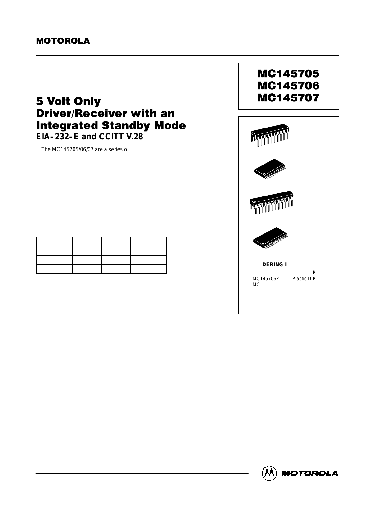
PIN ASSIGNMENTS
MC145706
3 DRIVERS/2 RECEIVERS
MC145705
2 DRIVERS/3 RECEIVERS
MC145707
3 DRIVERS/3 RECEIVERS
C2+
GND
C2–
V
SS
STB
Tx1
Rx1
Tx2
Rx2
Tx3
1
2
3
4
5
6
7
8
9
10
C1+
V
CC
C1–
V
DD
TxEN
DI1
DO1
DI2
DO2
DI3
20
19
18
17
16
15
14
13
12
11
1
2
3
4
5
6
7
8
9
10
20
19
18
17
16
15
14
13
12
11
C1+
V
CC
C1–
V
DD
TxEN
DO1
DO2
DI1
DO3
DI2
C2+
GND
C2–
V
SS
STB
Rx1
Rx2
Tx1
Rx3
Tx2
1
2
3
4
5
6
7
8
9
10
11
12
24
23
22
21
20
19
18
17
16
15
14
13
C2+
GND
C2–
V
SS
STB
NC
Rx1
Tx1
Rx2
Tx2
Rx3
Tx3
C1+
V
CC
C1–
V
DD
TxEN
NC
DO1
DI1
DO2
DI2
DO3
DI3
NC = NO CONNECTION
MC145705•MC145706•MC145707MOTOROLA
3
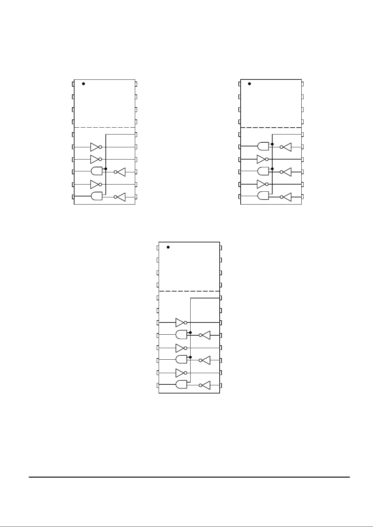
FUNCTION DIAGRAM
RECEIVER
DRIVER
TxEN
CHARGE PUMPS
OSC
VOLTAGE
DOUBLER
VOLTAGE
INVERTER
V
SS
V
DD
V
CC
GND
C1
C3 C4
C2
C1– C1+ C2+ C2–
+
+ +
+
–
+
V
DD
V
DD
V
SS
V
CC
STB
DO
1.0 V
1.8 V
15 k
Ω
5.4 k
Ω
*
*Protection Circuit
LEVEL
SHIFT
STB
V
CC
DI
1.4 V
–
+
V
CC
300
Ω
Tx
V
DD
V
SS
MC145705•MC145706•MC145707 MOTOROLA
4
MAXIMUM RATINGS (Voltage Polarities Referenced to GND)
Rating
Symbol Value Unit
DC Supply Voltage V
CC
– 0.5 to + 6.0 V
Input Voltage Rx1 – Rx3 Inputs
DI1 – DI3 Inputs
V
IR
VSS – 15 to VDD+ 15
0.5 to VCC+ 15
V
DC Current per Pin I ± 100 mA
Power Dissipation P
D
1 W
Operating Temperature Range T
A
– 40 to + 85 °C
Storage Temperature Range T
stg
– 85 to + 150 °C
RECOMMENDED OPERATING LIMITS
Parameter Symbol Min Typ Max Unit
Power Supply V
CC
4.5 5 5.5 V
Operating Temperature Range T
A
– 40 — 85 °C
DC ELECTRICAL CHARACTERISTICS (Voltage polarities referenced to GND = 0 V; C1 – C4 = 10 µF; T
A
= – 40 to + 85°C)
Parameter
Symbol Min Typ Max Unit
DC Power Supply V
CC
4.5 5 5.5 V
Quiescent Supply Current (Output Unloaded, Input Low) I
CC
— 1.7 3.5 mA
Quiescent Supply Current (Standby Mode) (Output Unloaded, Input Open) I
CC(STB)
— < 10 20 µA
Control Signal Input Voltage (STB, TxEN) Logic Low
Logic High
V
IL
V
IH
—
VCC – 0.5
—
—
0.5
—
V
Control Signal Input Current Logic Low (TxEN)
Logic High (STB)
I
IL
I
IH
—
—
—
—
– 10
10
µA
Charge Pumps Output Voltage (C1, C2, C3, C4 = 10 µF)
Output Voltage (VDD) I
load
= 0 mA
I
load
= 5 mA
I
load
= 10 mA
V
DD
8.5
7.5
6.0
10.0
9.5
9.0
11
—
—
V
Output Voltage (VSS) I
load
= 0 mA
I
load
= 5 mA
I
load
= 10 mA
V
SS
– 8.5
– 7.5
– 6.0
– 10.0
– 9.2
– 8.6
– 11
—
—
RECEIVER ELECTRICAL SPECIFICATIONS
(Voltage polarities referenced to GND = 0 V; VCC = + 5 V ± 10%; C1 – C4 = 10 µF; TA = – 40 to + 85°C)
Parameter
Symbol Min Typ Max Unit
Input Turn–On Threshold (V
DO1 – DO3
= VOL) Rx1 – Rx3 V
on
1.35 1.8 2.35 V
Input Turn–Off Threshold (V
DO1 – DO3
= VOH) Rx1 – Rx3 V
off
0.75 1 1.25 V
Input Threshold Hysteresis (Von = V
off
) Rx1 – Rx3 V
hys
0.6 0.8 — V
Input Resistance R
in
3 5.4 7 kΩ
High–Level Output Voltage (DO1 – DO3) I
out
= – 20 µA
V
Rx1 – Rx3
= – 3 to – 25 V I
out
= – 1 mA
V
OH
VCC – 0.1
VCC – 0.7
—
4.3
—
—
V
Low–Level Output Voltage (DO1 – DO3) I
out
= + 20 µA
V
Rx1 – Rx3
= + 3 to + 25 V I
out
= + 1.6 mA
V
OL
—
—
0.01
0.5
0.1
0.7
V
This device contains protection circuitry to
guard against damage due to high static
voltages or electric fields. However, precautions must be taken to avoid applications of any
voltage higher than maximum rated voltages to
this high–impedance circuit. For proper operation, it is recommended that the voltage at
the DI and DO pins be constrained to the range
GND ≤ VDI ≤ VDD and GND ≤ VDO ≤ VCC.
Also, the voltage at the Rx pin should be
constrained to (VSS – 15 V) ≤ V
Rx1 – Rx3
≤
(VDD + 15 V), and Tx should be constrained
to VSS ≤ V
Tx1 – Tx3
≤ VDD.
Unused inputs must always be tied to an
appropriate logic voltage level (e.g., GND or
VCC for DI, and GND for Rx).