

Motorola MC14568BCL, MC14568BCP, MC14568BD Datasheet
MOTOROLA CMOS LOGIC DATA
1
MC14568B
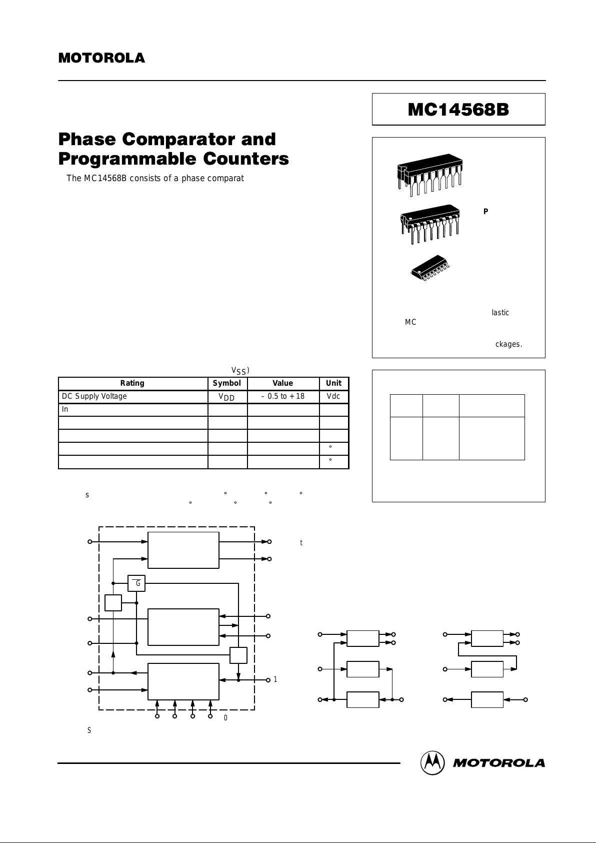
The MC14568B consists of a phase comparator, a divide–by–4, 16, 64 or
100 counter and a programmable divide–by–N 4–bit binary counter (all
positive–edge triggered) constructed with MOS P–channel and N–channel
enhancement mode devices (complementary MOS) in a monolithic structure.
The MC14568B has been designed for use i n conjunction with a
programmable divide–by–N counter for frequency synthesizers and phase–
locked loop applications requiring low power dissipation and/or high noise
immunity.
This device can be used with both counters cascaded and the output of
the second counter connected to the phase comparator (CTL high), or used
independently of the p rogrammable divide–by–N counter, for example
cascaded with a MC14569B, MC14522B or MC14526B (CTL low).
• Supply Voltage Range = 3.0 to 18 V
• Capable of Driving Two Low–Power TTL Loads, One Low–Power
Schottky TTL Load or Two HTL Loads Over the Rated Temperature
Range.
• Chip Complexity: 549 FETs or 137 Equivalent Gates
MAXIMUM RATINGS* (Voltages referenced to V
SS
)
Rating
Symbol Value Unit
DC Supply Voltage V
DD
– 0.5 to + 18 Vdc
Input Voltage, All Inputs V
in
– 0.5 to VDD + 0.5 Vdc
DC Input Current, per Pin I
in
± 10 mAdc
Power Dissipation, per Package† P
D
500 mW
Operating Temperature Range T
A
– 55 to + 125
_
C
Storage Temperature Range T
stg
– 65 to + 150
_
C
*Maximum Ratings are those values beyond which damage to the device may occur.
†Temperature Derating:
Plastic “P and D/DW” Packages: – 7.0 mW/_C From 65_C To 125_C
Ceramic “L” Packages: – 12 mW/_C From 100_C To 125_C
BLOCK DIAGRAM
PCin14
C1 9
CTL 15
“0” 3
PE 2
D
P3
D
P0
4 5 6 7
VDD = PIN 16
VSS = PIN 8
A
B
PHASE
COMPARATOR
13 PC
out
12 LD
11 G
10 F
1 Q1/C2
TG
TG
TG
COUNTER D1
4–BIT
PROGRAMMABLE
COUNTER D2
PC
in
C1
“0”
P/C
D1
D2
Q1/C2
Q1/C2
PC
out
LD
P/C
D1
D2
C1
“0”
DP2D
P1
(REF.)
CTL HIGH CTL LOW
PC
in
PC
out
LD
SEMICONDUCTOR TECHNICAL DATA
Motorola, Inc. 1995
REV 3
1/94
L SUFFIX
CERAMIC
CASE 620
ORDERING INFORMATION
MC14XXXBCP Plastic
MC14XXXBCL Ceramic
MC14XXXBD SOIC
TA = – 55° to 125°C for all packages.
P SUFFIX
PLASTIC
CASE 648
D SUFFIX
SOIC
CASE 751B
TRUTH TABLE
F G Division Ratio
Pin 10 Pin 11 of Counter D1
0 0 4
0 1 16
1 0 64
1 1 100
The divide by zero state on the programmable divide–by–N 4–bit binary
counter, D2, is illegal.
MOTOROLA CMOS LOGIC DATAMC14568B
2
ELECTRICAL CHARACTERISTICS (Voltages Referenced to V
SS
)
V
– 55_C 25_C 125_C
Characteristic
Symbol
V
DD
Vdc
Min Max Min Typ # Max Min Max
Unit
Output Voltage “0” Level
Vin = VDD or 0
V
OL
5.0
10
15
—
—
—
0.05
0.05
0.05
—
—
—
0
0
0
0.05
0.05
0.05
—
—
—
0.05
0.05
0.05
Vdc
“1” Level
Vin = 0 or V
DD
V
OH
5.0
10
15
4.95
9.95
14.95
—
—
—
4.95
9.95
14.95
5.0
10
15
—
—
—
4.95
9.95
14.95
—
—
—
Vdc
Input Voltage#‡ “0” Level
(VO = 4.5 or 0.5 Vdc)
(VO = 9.0 or 1.0 Vdc)
(VO = 13.5 or 1.5 Vdc)
V
IL
5.0
10
15
—
—
—
1.5
3.0
4.0
—
—
—
2.25
4.50
6.75
1.5
3.0
4.0
—
—
—
1.5
3.0
4.0
Vdc
“1” Level
(VO = 0.5 or 4.5 Vdc)
(VO = 1.0 or 9.0 Vdc)
(VO = 1.5 or 13.5 Vdc)
V
IH
5.0
10
15
3.5
7.0
11
—
—
—
3.5
7.0
11
2.75
5.50
8.25
—
—
—
3.5
7.0
11
—
—
—
Vdc
Output Drive Current
(VOH = 2.5 Vdc) Source
(VOH = 4.6 Vdc)
(VOH = 9.5 Vdc)
(VOH = 13.5 Vdc)
I
OH
5.0
5.0
10
15
– 1.2
– 0.25
– 0.62
– 1.8
—
—
—
—
– 1.0
– 0.2
– 0.5
– 1.5
– 1.7
– 0.36
– 0.9
– 3.5
—
—
—
—
– 0.7
– 0.14
– 0.35
– 1.1
—
—
—
—
mAdc
(VOL = 0.4 Vdc) Sink
(VOL = 0.5 Vdc)
(VOL = 1.5 Vdc)
I
OL
5.0
10
15
0.64
1.6
4.2
—
—
—
0.51
1.3
3.4
0.88
2.25
8.8
—
—
—
0.36
0.9
2.4
—
—
—
mAdc
Input Current I
in
15 — ±0.1 — ±0.00001 ±0.1 — ±1.0 µAdc
Input Capacitance C
in
— — — — 5.0 7.5 — — pF
Quiescent Current
(Per Package) Vin = 0 or VDD,
I
out
= 0 µA
I
DD
5.0
10
15
—
—
—
5.0
10
20
—
—
—
0.005
0.010
0.015
5.0
10
20
—
—
—
150
300
600
µAdc
Total Supply Current**†
(Dynamic plus Quiescent,
Per Package)
(CL = 50 pF on all outputs, all
buffers switching)
I
T
5.0
10
15
IT = (0.2 µA/kHz) f + I
DD
IT = (0.4 µA/kHz) f + I
DD
IT = (0.9 µA/kHz) f + I
DD
µAdc
Three–State Leakage Current
Pins 1, 13
I
TL
15 — ±0.1 — ±0.0001 ±0.1 — ±3.0 µAdc
#Noise immunity for worst input combination.
Noise Margin for both “1” and “0” level = 1.0 V min @ VDD = 5.0 V
= 2.0 V min @ VDD = 10 V
= 2.5 V min @ VDD = 15 V
†To calculate total supply current at loads other than 50 pF:
IT(CL) = IT(50 pF) + 1 x 10⁻³ (CL – 50) VDDf
where: IT is in µA (per package), CL in pF, VDD in V, and f in kHz is input frequency.
**The formulas given are for the typical characteristics only at 25_C.
‡Pin 15 is connected to VSS or VDD for input voltage test.
PIN ASSIGNMENT
13
14
15
16
9
10
11
125
4
3
2
1
8
7
6
LD
PC
out
PC
in
CTL
V
DD
C1
F
G
D
P3
“0”
PE
Q1/C2
V
SS
D
P0
D
P1
D
P2
MOTOROLA CMOS LOGIC DATA
3
MC14568B
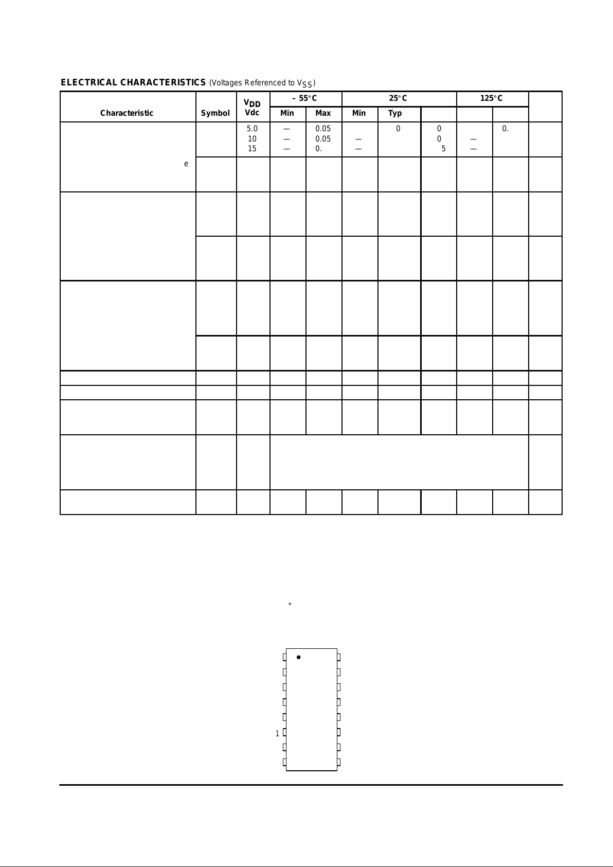
SWITCHING CHARACTERISTICS (C
L
= 50 pF, TA = 25_C)
Characteristic
Symbol
V
DD
V
Min Typ Max Unit
Output Rise Time t
TLH
5.0
10
15
—
—
—
180
90
65
360
180
130
ns
Output Fall Time t
THL
5.0
10
15
—
—
—
100
50
40
200
100
80
ns
Minimum Pulse Width, C1, Q1/C2, or PCin Input t
WH
5.0
10
15
—
—
—
125
60
45
250
120
90
ns
Maximum Clock Rise and Fall Time,
C1, Q1/C2, or PCin Input
t
TLH
,
t
THL
5.0
10
15
15
15
15
—
—
—
—
—
—
µs
PHASE COMPARATOR
Input Resistance R
in
5.0 to 15 — 10
6
— MΩ
Input Sensitivity, dc Coupled — 5.0 to 15 See Input Voltage
Turn–Off Delay Time,
PC
out
and LD Outputs
t
PHL
5.0
10
15
—
—
—
550
195
120
1100
390
240
ns
Turn–On Delay Time.
PC
out
and LD Outputs
t
PLH
5.0
10
15
—
—
—
675
300
190
1350
600
380
ns
DIVIDE–BY–4, 16, 64 OR 100 COUNTER (D1)
Maximum Clock Pulse Frequency
Division Ratio = 4, 64 or 100
f
cl
5.0
10
15
3.0
8.0
10
6.0
16
22
—
—
—
MHz
Division Ratio = 16 5.0
10
15
1.0
3.0
5 0
2.5
6.3
9.7
—
—
—
Propagation Delay Time, Q1/C2 Output
Division Ratio = 4, 64 or 100
t
PLH
,
t
PHL
5.0
10
15
—
—
—
450
190
130
900
380
260
ns
Division Ratio = 16 5.0
10
15
—
—
—
720
300
200
1440
600
400
PROGRAMMABLE DIVIDE–BY–N 4–BIT COUNTER (D2)
Maximum Clock Pulse Frequency
(Figure 3a)
f
cl
5.0
10
15
1.2
3.0
4.0
1.8
8.5
12
—
—
—
MHz
Turn–On Delay Time, “0” Output
(Figure 3a)
t
PLH
5.0
10
15
—
—
—
450
190
130
900
380
260
ns
Turn–Off Delay Time, “0” Output
(Figure 3a)
t
PHL
5.0
10
15
—
—
—
225
85
60
450
170
150
ns
Minimum Preset Enable Pulse Width t
WH(PE)
5.0
10
15
—
—
—
75
40
30
250
100
75
ns
MOTOROLA CMOS LOGIC DATAMC14568B
4
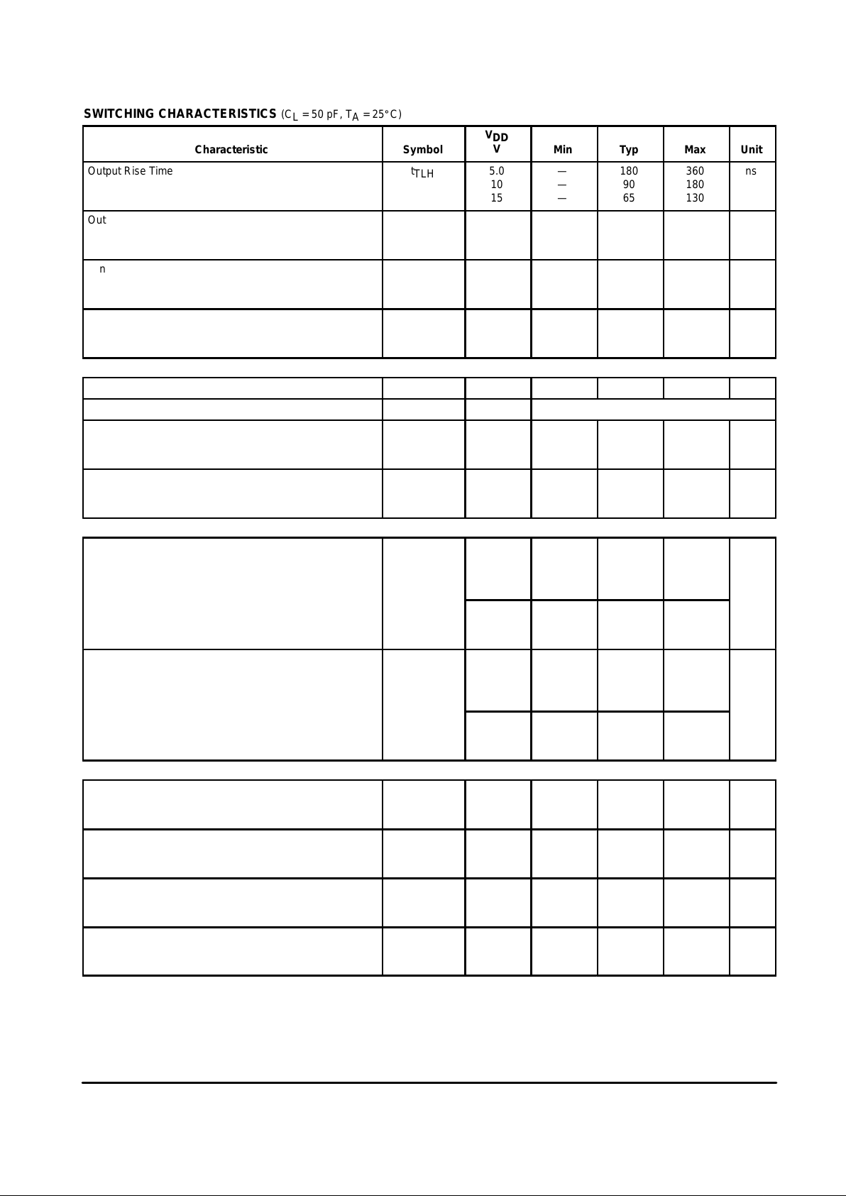
Figure 1. Phase Comparator
DP0PC
out
PULSE
GENERATOR 2
PULSE
GENERATOR 1
“0”
out
REF
PULSE
GENERATOR
PULSE
GENERATOR
PULSE
GENERATOR 1
PULSE
GENERATOR 2
Figure 2. Counter D1
Figure 3. Counter D2
*N is the value programmed on the DP Inputs.
V
DD
V
DD
2
10 k
C
L
C
L
LD
Q1/C2
“0”
V
SS
CTL
D
P1
D
P2
D
P3
PC
in
F
G
C1
PE
A LAGS B, PC
out
IS LOW. A LEADS B, PC
out
IS HIGH.
50%
20 ns
20 ns
t
W(PCin)
90%
50%
10%
t
PLH
t
PLH
t
THL
90%
10%
t
PHL
t
PHL
t
TLH
THREE–STATE THREE–STATE 75%
t
PLH
t
PHL
25%
V
OH
V
OL
PC
in
PG1
LD
PC
out
B
A
V
DD
V
SS
C
L
D
P0
CTL
D
P1
D
P2
D
P3
PC
in
F
G
C1
PE
PC
out
LD
Q1/C2
“0”
20 ns
20 ns
t
W(C1)
t
PHL
10%
50%
90%
t
TLHtTHL
finf
max
90%
50%
10%
C1
Q1/C2
D
P0
D
P1
D
P2
D
P3
PC
in
F
G
C1
PE
CTL
Q1/C2
PC
out
LD
“0”
V
SS
V
DD
a. b.
C
L
D
P0
D
P1
D
P2
D
P3
PC
in
F
G
C1
PE
CTL
Q1/C2
PC
out
LD
“0”
C
L
V
SS
V
DD
t
W(Q1/C2)
20 ns20 ns
90%
50%
10%
90%
50%
10%
Q1/C2
“0”
finf
max
t
PHL
t
PLH
t
TLH
t
THL
N PULSES*
Q1/C2 = PG 1
PE = PG2
20 ns
20 ns
50%
90%
50%
10%
t
W(PE)
“0”
SWITCHING TIME TEST CIRCUITS AND WAVEFORMS
t
PLH
 Loading...