

Datasheet MC14543BF, MC14543BFEL, MC14543BDR2, MC14543BCP, MC14543BFL1 Datasheet (MOTOROLA)
...
Semiconductor Components Industries, LLC, 2000
March, 2000 – Rev. 3
1 Publication Order Number:
MC14543B/D
MC14543B
BCD-to-Seven Segment
Latch/Decoder/Driver for
Liquid Crystals
The MC14543B BCD–to–seven segment latch/decoder/driver is
designed for use with liquid crystal readouts, and is constructed with
complementary MOS (CMOS) enhancement mode devices. The
circuit provides the functions of a 4–bit storage latch and an 8421
BCD–to–seven segment decoder and driver. The device has the
capability to invert the logic levels of the output combination. The
phase (Ph), blanking (BI), and latch disable (LD) inputs are used to
reverse the truth table phase, blank the display , and store a BCD code,
respectively . For liquid crystal (LC) readouts, a square wave is applied
to the Ph input of the circuit and the electrically common backplane of
the display. The outputs of the circuit are connected directly to the
segments of the LC readout. For other types of readouts, such as
light–emitting diode (LED), incandescent, gas discharge, and
fluorescent readouts, connection diagrams are given on this data sheet.
Applications include instrument (e.g., counter, DVM etc.) display
driver, computer/calculator display driver, cockpit display driver, and
various clock, watch, and timer uses.
• Latch Storage of Code
• Blanking Input
• Readout Blanking on All Illegal Input Combinations
• Direct LED (Common Anode or Cathode) Driving Capability
• Supply Voltage Range = 3.0 V to 18 V
• Capable of Driving 2 Low–power TTL Loads, 1 Low–power Schottky
TTL Load or 2 HTL Loads Over the Rated Temperature Range
• Pin–for–Pin Replacement for CD4056A (with Pin 7 Tied to V
SS
).
• Chip Complexity: 207 FETs or 52 Equivalent Gates
MAXIMUM RATINGS (Voltages Referenced to V
SS
) (Note 2.)
Symbol Parameter Value Unit
V
DD
DC Supply Voltage Range –0.5 to +18.0 V
V
in
Input Voltage Range, All Inputs –0.5 to VDD + 0.5 V
I
in
DC Input Current per Pin ±10 mA
P
D
Power Dissipation,
per Package (Note 3.)
500 mW
T
A
Operating Temperature Range –55 to +125 °C
T
stg
Storage Temperature Range –65 to +150 °C
I
OHmax
I
OLmax
Maximum Continuous Output
Drive Current (Source or Sink)
10
(per Output)
mA
P
OHmax
P
OLmax
Maximum Continuous Output
Power (Source or Sink)
(4.)
70
(per Output)
mW
2. Maximum Ratings are those values beyond which damage to the device
may occur.
3. Temperature Derating:
Plastic “P and D/DW” Packages: – 7.0 mW/_C From 65_C T o 125_C
4. P
OHmax
= IOH (VOH – VDD) and P
OLmax
= IOL (VOL – VSS)
http://onsemi.com
A = Assembly Location
WL or L = Wafer Lot
YY or Y = Year
WW or W = Work Week
Device Package Shipping
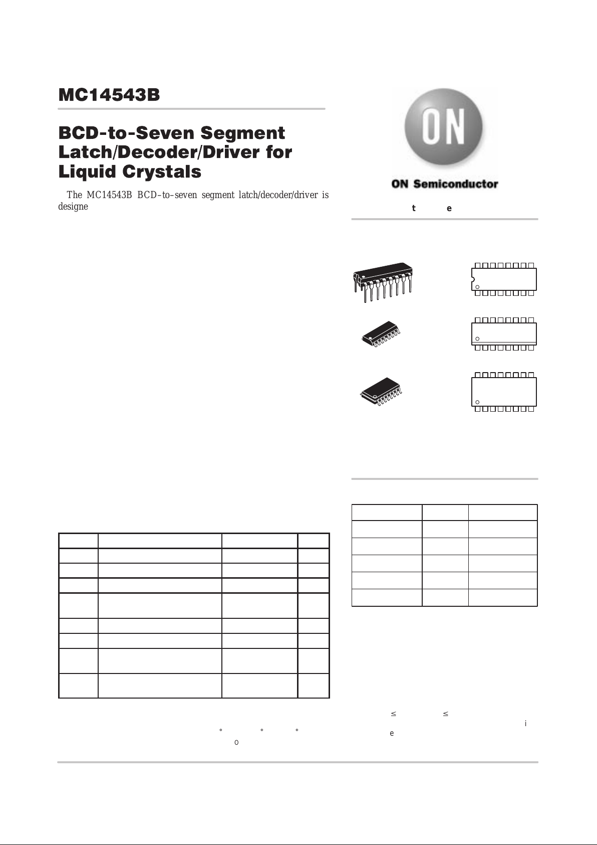
ORDERING INFORMATION
MC14543BCP PDIP–16 2000/Box
MC14543BD SOIC–16 48/Rail
MC14543BDR2 SOIC–16 2500/Tape & Reel
1. For ordering information on the EIAJ version of
the SOIC packages, please contact your local
ON Semiconductor representative.
MARKING
DIAGRAMS
1
16
PDIP–16
P SUFFIX
CASE 648
MC14543BCP
AWLYYWW
SOIC–16
D SUFFIX
CASE 751B
1
16
14543B
AWLYWW
SOEIAJ–16
F SUFFIX
CASE 966
1
16
MC14543B
AWLYWW
MC14543BFEL SOEIAJ–16 See Note 1.
MC14543BF SOEIAJ–16 See Note 1.
This device contains protection circuitry to guard
against damage due to high static voltages or electric
fields. However, precautions must be taken to avoid applications of any voltage higher than maximum rated
voltages to this high–impedance circuit. For proper
operation, V
in
and V
out
should be constrained to the
range V
SS
v (Vin or V
out
) v VDD.
Unused inputs must always be tied to an appropriate
logic voltage level (e.g., either V
SS
or VDD). Unused out-
puts must be left open.
MC14543B
http://onsemi.com
2
TRUTH TABLE
Inputs Outputs
LD BI Ph* D C B A a b c d e f g Display
X 1 0 X X X X 0 0 0 0 0 0 0 Blank
1 0 0 00 001111110 0
1 0 0 00 010110000 1
1 0 0 00 101101101 2
1 0 0 00 111111001 3
1 0 0 01 000110011 4
1 0 0 01 011011011 5
1 0 0 01 101011111 6
1 0 0 01 111110000 7
1 0 0 10 001111111 8
1 0 0 10 011111011 9
1 0 0 1 0 1 0 0 0 0 0 0 0 0 Blank
1 0 0 1 0 1 1 0 0 0 0 0 0 0 Blank
1 0 0 1 1 0 0 0 0 0 0 0 0 0 Blank
1 0 0 1 1 0 1 0 0 0 0 0 0 0 Blank
1 0 0 1 1 1 0 0 0 0 0 0 0 0 Blank
1 0 0 1 1 1 1 0 0 0 0 0 0 0 Blank
000XXXX ** **
† † † † Inverse of Output Display
Combinations as above
Above
X = Don’t care
† = Above Combinations
* = For liquid crystal readouts, apply a square wave to Ph
For common cathode LED readouts, select Ph = 0
For common anode LED readouts, select Ph = 1
** = Depends upon the BCD code previously applied when LD = 1
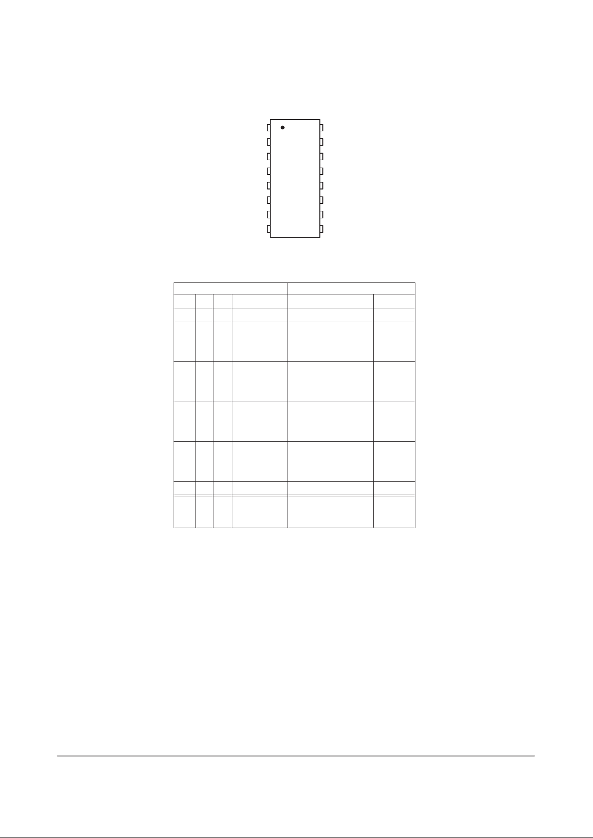
PIN ASSIGNMENT
13
14
15
16
9
10
11
125
4
3
2
1
8
7
6
d
e
g
f
V
DD
a
b
c
D
B
C
LD
V
SS
BI
PH
A
MC14543B
http://onsemi.com
3
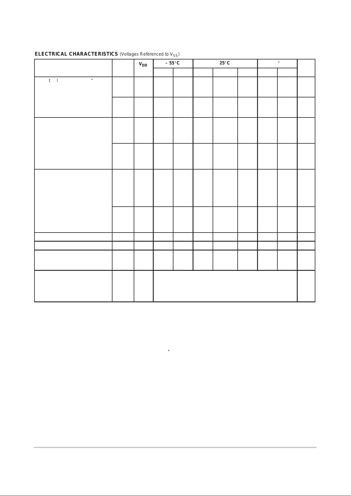
ELECTRICAL CHARACTERISTICS (Voltages Referenced to V
SS
)
V
DD
– 55_C 25_C 125_C
Characteristic Symbol
Vdc
Min Max Min Typ
(5.)
Max Min Max
Unit
Output Voltage “0” Level
V
in
= VDD or 0
V
OL
5.0
10
15
—
—
—
0.05
0.05
0.05
—
—
—
0
0
0
0.05
0.05
0.05
—
—
—
0.05
0.05
0.05
Vdc
“1” Level
V
in
= 0 or V
DD
V
OH
5.0
10
15
4.95
9.95
14.95
—
—
—
4.95
9.95
14.95
5.0
10
15
—
—
—
4.95
9.95
14.95
—
—
—
Vdc
Input Voltage “0” Level
(V
O
= 4.5 or 0.5 Vdc)
(V
O
= 9.0 or 1.0 Vdc)
(V
O
= 13.5 or 1.5 Vdc)
V
IL
5.0
10
15
—
—
—
1.5
3.0
4.0
—
—
—
2.25
4.50
6.75
1.5
3.0
4.0
—
—
—
1.5
3.0
4.0
Vdc
“1” Level
(V
O
= 0.5 or 4.5 Vdc)
(V
O
= 1.0 or 9.0 Vdc)
(V
O
= 1.5 or 13.5 Vdc)
V
IH
5.0
10
15
3.5
7.0
11
—
—
—
3.5
7.0
11
2.75
5.50
8.25
—
—
—
3.5
7.0
11
—
—
—
Vdc
Output Drive Current
(V
OH
= 2.5 Vdc) Source
(V
OH
= 4.6 Vdc)
(V
OH
= 0.5 Vdc)
(V
OH
= 9.5 Vdc)
(V
OH
= 13.5 Vdc)
I
OH
5.0
5.0
10
10
15
– 3.0
– 0.64
—
– 1.6
– 4.2
—
—
—
—
—
– 2.4
– 0.51
—
– 1.3
– 3.4
– 4.2
– 0.88
– 10.1
– 2.25
– 8.8
—
—
—
—
—
– 1.7
– 0.36
—
– 0.9
– 2.4
—
—
—
—
mAdc
(VOL = 0.4 Vdc) Sink
(V
OL
= 0.5 Vdc)
(V
OL
= 9.5 Vdc)
(V
OL
= 1.5 Vdc)
I
OL
5.0
10
10
15
0.64
1.6
—
4.2
—
—
—
—
0.51
1.3
—
3.4
0.88
2.25
10.1
8.8
—
—
—
—
0.36
0.9
—
2.4
—
—
—
mAdc
Input Current I
in
15 — ±0.1 — ±0.00001 ±0.1 — ±1.0 µAdc
Input Capacitance C
in
— — — — 5.0 7.5 — — pF
Quiescent Current
(Per Package) V
in
= 0 or VDD,
I
out
= 0 µA
I
DD
5.0
10
15
—
—
—
5.0
10
20
—
—
—
0.005
0.010
0.015
5.0
10
20
—
—
—
150
300
600
µAdc
Total Supply Current
(6.) (7.)
(Dynamic plus Quiescent,
Per Package)
(C
L
= 50 pF on all outputs, all
buffers switching)
I
T
5.0
10
15
IT = (1.6 µA/kHz) f + I
DD
IT = (3.1 µA/kHz) f + I
DD
IT = (4.7 µA/kHz) f + I
DD
µAdc
5. Noise immunity specified for worst–case input combination.
Noise Margin for both “1” and “0” level = 1.0 V min @ V
DD
= 5.0 V
= 2.0 V min @ V
DD
= 10 V
= 2.5 V min @ V
DD
= 15 V
6. To calculate total supply current at loads other than 50 pF:
IT(CL) = IT(50 pF) + 3.5 x 10⁻³ (CL – 50) VDDf
where: I
T
is in µA (per package), CL in pF, VDD in V, and f in kHz is input frequency.
7. The formulas given are for the typical characteristics only at 25_C.

MC14543B
http://onsemi.com
4
SWITCHING CHARACTERISTICS
(8.)
(C
L
= 50 pF, T
A
= 25_C)
Characteristic
Symbol V
DD
Min Typ Max Unit
Output Rise Time
t
TLH
= (3.0 ns/pF) CL + 30 ns
t
TLH
= (1.5 ns/pF) CL + 15 ns
t
TLH
= (1.1 ns/pF) CL + 10 ns
t
TLH
5.0
10
15
—
—
—
100
50
40
200
100
80
ns
Output Fall Time
t
THL
= (1.5 ns/pF) CL + 25 ns
t
THL
= (0.75 ns/pF) CL + 12.5 ns
t
THL
= (0.55 ns/pF) CL + 12.5 ns
t
THL
5.0
10
15
—
—
—
100
50
40
200
100
80
ns
Turn–Off Delay Time
t
PLH
= (1.7 ns/pF) CL + 520 ns
t
PLH
= (0.66 ns/pF) CL + 217 ns
t
PLH
= (0.5 ns/pF) CL + 160 ns
t
PLH
5.0
10
15
—
—
—
605
250
185
1210
500
370
ns
Turn–On Delay Time
t
PHL
= (1.7 ns/pF) CL + 420 ns
t
PHL
= (0.66 ns/pF) CL + 172 ns
t
PHL
= (0.5 ns/pF) CL + 130 ns
t
PHL
5.0
10
15
—
—
—
505
205
155
1650
660
495
ns
Setup Time t
su
5.0
10
15
350
450
500
—
—
—
ns
Hold Time t
h
5.0
10
15
40
30
20
—
—
—
ns
Latch Disable Pulse Width (Strobing Data) t
WH
5.0
10
15
250
100
80
125
50
40
—
—
—
ns
8. The formulas given are for the typical characteristics only.
LOGIC DIAGRAM
VDD = PIN 16
V
SS
= PIN 8
B3
LD 1
D4
C2
A5
PHASE 6
14 g
15 f
13 e
12 d
11 c
10 b
9a
BI 7

MC14543B
http://onsemi.com
5
Figure 1. Typical Output Source
Characteristics
Figure 2. Typical Output Sink
Characteristics
–24
–18
–12
–6.0
0
I
OH
, SOURCE CURRENT (mAdc)
(VOH – VDD), SOURCE DEVICE VOLTAGE (Vdc)
–16 –12 –8.0 –4.0 0
VDD = 5.0 Vdc
P
OHmax
= 70 mWdc
VDD = 10 Vdc
VDD = 15 Vdc
VSS = 0 Vdc
0
6.0
12
18
24
I
OL
, SINK CURRENT (mAdc)
(VOL – VSS), SINK DEVICE VOLTAGE (Vdc)
0 4.0 8.0 12 16
VDD = 15 Vdc
VDD = 10 Vdc
VDD = 5.0 Vdc
VSS = 0 Vdc
P
OLmax
= 70 mWdc
Figure 3. Dynamic Power Dissipation
Signal Waveforms
Inputs BI and Ph low, and Inputs D and LD high.
f in respect to a system clock.
Figure 4. Dynamic Signal Waveforms
(a) Inputs D, Ph, and BI low, and Inputs A, B, and LD high.
(b) Inputs D, Ph, and BI low, and Inputs A and B high.
(c) Data DCBA strobed into latches
20 ns
20 ns
V
DD
V
SS
V
OH
V
OL
10%
50%
90%
1
2f
50% DUTY CYCLE
A, B, AND C
ANY OUTPUT
All outputs connected to respective C
L
loads.
20 ns 20 ns
90%
10%
50%
t
PHL
t
PLH
90%
50%
10%
V
DD
V
SS
V
OH
V
OL
V
DD
V
SS
V
DD
V
SS
V
OH
V
OL
V
DD
V
SS
t
THL
t
TLH
C
g
LD
C
g
LD
20 ns
90%
50%
10%
50% 50%
t
h
t
su
50%
t
WH

MC14543B
http://onsemi.com
6
CONNECTIONS TO VARIOUS DISPLAY READOUTS
LIQUID CRYSTAL (LC) READOUT
LIGHT EMITTING DIODE (LED) READOUT
INCANDESCENT READOUT
NOTE: Bipolar transistors may be added for gain (for VDD v 10 V or I
out
≥ 10 mA).
GAS DISCHARGE READOUT
CONNECTIONS TO SEGMENTS
SQUARE WAVE
(V
SS
TO VDD)
COMMON
BACKPLANE
ONE OF SEVEN SEGMENTS
MC14543B
OUTPUT
Ph
MC14543B
OUTPUT
Ph
V
SS
APPROPRIATE
VOLTAGE
MC14543B
OUTPUT
Ph
V
SS
COMMON
CATHODE LED
COMMON
ANODE LED
V
DD
MC14543B
OUTPUT
Ph
V
DD
MC14543B
OUTPUT
Ph
APPROPRIATE
VOLTAGE
V
SS
VDD = PIN 16
V
SS
= PIN 8
0123456789
DISPLAY
a
b
c
d
e
fg

MC14543B
http://onsemi.com
7
P ACKAGE DIMENSIONS
PDIP–16
P SUFFIX
PLASTIC DIP PACKAGE
CASE 648–08
ISSUE R
NOTES:
1. DIMENSIONING AND TOLERANCING PER ANSI
Y14.5M, 1982.
2. CONTROLLING DIMENSION: INCH.
3. DIMENSION L TO CENTER OF LEADS WHEN
FORMED PARALLEL.
4. DIMENSION B DOES NOT INCLUDE MOLD FLASH.
5. ROUNDED CORNERS OPTIONAL.
–A–
B
F
C
S
H
G
D
J
L
M
16 PL
SEATING
18
916
K
PLANE
–T–
M
A
M
0.25 (0.010) T
DIM MIN MAX MIN MAX
MILLIMETERSINCHES
A 0.740 0.770 18.80 19.55
B 0.250 0.270 6.35 6.85
C 0.145 0.175 3.69 4.44
D 0.015 0.021 0.39 0.53
F 0.040 0.70 1.02 1.77
G 0.100 BSC 2.54 BSC
H 0.050 BSC 1.27 BSC
J 0.008 0.015 0.21 0.38
K 0.110 0.130 2.80 3.30
L 0.295 0.305 7.50 7.74
M 0 10 0 10
S 0.020 0.040 0.51 1.01
____
SOIC–16
D SUFFIX
PLASTIC SOIC PACKAGE
CASE 751B–05
ISSUE J
NOTES:
1. DIMENSIONING AND TOLERANCING PER ANSI
Y14.5M, 1982.
2. CONTROLLING DIMENSION: MILLIMETER.
3. DIMENSIONS A AND B DO NOT INCLUDE
MOLD PROTRUSION.
4. MAXIMUM MOLD PROTRUSION 0.15 (0.006)
PER SIDE.
5. DIMENSION D DOES NOT INCLUDE DAMBAR
PROTRUSION. ALLOWABLE DAMBAR
PROTRUSION SHALL BE 0.127 (0.005) TOTAL
IN EXCESS OF THE D DIMENSION AT
MAXIMUM MATERIAL CONDITION.
18
16 9
SEATING
PLANE
F
J
M
R
X 45
_
G
8 PLP
–B–
–A–
M
0.25 (0.010) B
S
–T–
D
K
C
16 PL
S
B
M
0.25 (0.010) A
S
T
DIM MIN MAX MIN MAX
INCHESMILLIMETERS
A 9.80 10.00 0.386 0.393
B 3.80 4.00 0.150 0.157
C 1.35 1.75 0.054 0.068
D 0.35 0.49 0.014 0.019
F 0.40 1.25 0.016 0.049
G 1.27 BSC 0.050 BSC
J 0.19 0.25 0.008 0.009
K 0.10 0.25 0.004 0.009
M 0 7 0 7
P 5.80 6.20 0.229 0.244
R 0.25 0.50 0.010 0.019
____

MC14543B
http://onsemi.com
8
P ACKAGE DIMENSIONS
H
E
A
1
DIM MIN MAX MIN MAX
INCHES
––– 2.05 ––– 0.081
MILLIMETERS
0.05 0.20 0.002 0.008
0.35 0.50 0.014 0.020
0.18 0.27 0.007 0.011
9.90 10.50 0.390 0.413
5.10 5.45 0.201 0.215
1.27 BSC 0.050 BSC
7.40 8.20 0.291 0.323
0.50 0.85 0.020 0.033
1.10 1.50 0.043 0.059
0
0.70 0.90 0.028 0.035
––– 0.78 ––– 0.031
A
1
H
E
Q
1
L
E
_
10
_
0
_
10
_
L
E
Q
1
_
NOTES:
1. DIMENSIONING AND TOLERANCING PER ANSI
Y14.5M, 1982.
2. CONTROLLING DIMENSION: MILLIMETER.
3. DIMENSIONS D AND E DO NOT INCLUDE
MOLD FLASH OR PROTRUSIONS AND ARE
MEASURED AT THE PARTING LINE. MOLD FLASH
OR PROTRUSIONS SHALL NOT EXCEED 0.15
(0.006) PER SIDE.
4. TERMINAL NUMBERS ARE SHOWN FOR
REFERENCE ONLY.
5. THE LEAD WIDTH DIMENSION (b) DOES NOT
INCLUDE DAMBAR PROTRUSION. ALLOWABLE
DAMBAR PROTRUSION SHALL BE 0.08 (0.003)
TOTAL IN EXCESS OF THE LEAD WIDTH
DIMENSION AT MAXIMUM MATERIAL CONDITION.
DAMBAR CANNOT BE LOCATED ON THE LOWER
RADIUS OR THE FOOT. MINIMUM SPACE
BETWEEN PROTRUSIONS AND ADJACENT LEAD
TO BE 0.46 ( 0.018).
M
L
DETAIL P
VIEW P
c
A
b
e
M
0.13 (0.005)
0.10 (0.004)
1
16 9
8
D
Z
E
A
b
c
D
E
e
L
M
Z
SOEIAJ–16
F SUFFIX
PLASTIC EIAJ SOIC PACKAGE
CASE 966–01
ISSUE O
ON Semiconductor and are trademarks of Semiconductor Components Industries, LLC (SCILLC). SCILLC reserves the right to make changes
without further notice to any products herein. SCILLC makes no warranty , representation or guarantee regarding the suitability of its products for any particular
purpose, nor does SCILLC assume any liability arising out of the application or use of any product or circuit, and specifically disclaims any and all liability ,
including without limitation special, consequential or incidental damages. “Typical” parameters which may be provided in SCILLC data sheets and/or
specifications can and do vary in different applications and actual performance may vary over time. All operating parameters, including “Typicals” must be
validated for each customer application by customer’s technical experts. SCILLC does not convey any license under its patent rights nor the rights of others.
SCILLC products are not designed, intended, or authorized for use as components in systems intended for surgical implant into the body, or other applications
intended to support or sustain life, or for any other application in which the failure of the SCILLC product could create a situation where personal injury or
death may occur. Should Buyer purchase or use SCILLC products for any such unintended or unauthorized application, Buyer shall indemnify and hold
SCILLC and its officers, employees, subsidiaries, affiliates, and distributors harmless against all claims, costs, damages, and expenses, and reasonable
attorney fees arising out of, directly or indirectly , any claim of personal injury or death associated with such unintended or unauthorized use, even if such claim
alleges that SCILLC was negligent regarding the design or manufacture of the part. SCILLC is an Equal Opportunity/Affirmative Action Employer .
PUBLICATION ORDERING INFORMATION
CENTRAL/SOUTH AMERICA:
Spanish Phone: 303–308–7143 (Mon–Fri 8:00am to 5:00pm MST)
Email: ONlit–spanish@hibbertco.com
ASIA/PACIFIC : LDC for ON Semiconductor – Asia Support
Phone: 303–675–2121 (Tue–Fri 9:00am to 1:00pm, Hong Kong Time)
T oll Free from Hong Kong & Singapore:
001–800–4422–3781
Email: ONlit–asia@hibbertco.com
JAPAN: ON Semiconductor, Japan Customer Focus Center
4–32–1 Nishi–Gotanda, Shinagawa–ku, T okyo, Japan 141–8549
Phone: 81–3–5740–2745
Email: r14525@onsemi.com
ON Semiconductor Website: http://onsemi.com
For additional information, please contact your local
Sales Representative.
MC14543B/D
NORTH AMERICA Literature Fulfillment:
Literature Distribution Center for ON Semiconductor
P.O. Box 5163, Denver, Colorado 80217 USA
Phone: 303–675–2175 or 800–344–3860 T oll Free USA/Canada
Fax: 303–675–2176 or 800–344–3867 Toll Free USA/Canada
Email: ONlit@hibbertco.com
Fax Response Line: 303–675–2167 or 800–344–3810 T oll Free USA/Canada
N. American Technical Support: 800–282–9855 Toll Free USA/Canada
EUROPE: LDC for ON Semiconductor – European Support
German Phone: (+1) 303–308–7140 (M–F 1:00pm to 5:00pm Munich Time)
Email: ONlit–german@hibbertco.com
French Phone: (+1) 303–308–7141 (M–F 1:00pm to 5:00pm Toulouse T ime)
Email: ONlit–french@hibbertco.com
English Phone: (+1) 303–308–7142 (M–F 12:00pm to 5:00pm UK Time)
Email: ONlit@hibbertco.com
EUROPEAN TOLL–FREE ACCESS*: 00–800–4422–3781
*Available from Germany, France, Italy , England, Ireland
 Loading...