

MC145421•MC145425MOTOROLA
1
(UDLT II)
The MC145421 and MC145425 UDLTs are high–speed data transceivers
capable of providing 160 kbps full–duplex data communication over 26 AWG
and larger twisted–pair cable up to 1 km in length. These devices are primarily
used in digital subscriber voice and data telephone systems. In addition, the
devices meet and exceed the CCITT recommendations for data transfer rates
of ISDNs on a single twisted pair. The devices utilize a 512 kbaud MDPSK burst
modulation technique to supply the 160 kbps full–duplex data transfer rates.
The 160 kbps rate is provided through four channels. There are two B channels,
which are 64 kbps each. In addition, there are two D channels which are
16 kbps each.
The MC145421 and MC145425 UDL Ts are designed for upward compatibility
with the existing MC145422 and MC145426 80 kbps UDLTs, as well as compa–
tibility with existing and evolving telephone switching hardware and software
architectures.
The MC145421 (Master) UDLT is designed for use at the telephone switch
line card while the MC145425 (Slave) UDLT is designed for use at the remote
digital telset or data terminal.
• Employs CMOS Technology in Order to Take Advantage of Its Proven
Capability for Complex Analog and Digital LSI Functions
• Provides Synchronous Full–Duplex 160 kbps Voice and Data
Communication in a 2B+2D Format for ISDN Compatibility
• Provides the CCITT Basic Access Data Transfer Rate (2B+D) for ISDNs
on a Single Twisted Pair Up to 1 km
• Compatible with Existing and Evolving Telephone Switch Architectures and
Call Signaling Schemes
• Protocol Independent
• Single + 5 V Power Supply
• MC145421EVK is Available
16 kbps D2
64 kbps B1
64 kbps B2
16 kbps D1
16 kbps D2
64 kbps B1
64 kbps B2
TWISTED PAIR
WIRE
≤
1 km
MASTER
ISDN UDLT
160 kbps FULL–DUPLEX
DATA TRANSMISSION
SLAVE
ISDN UDLT
16 kbps D1
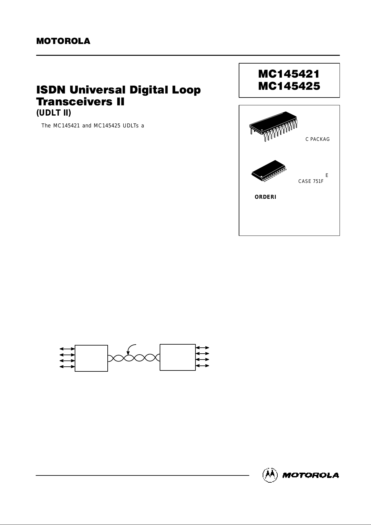
Order this document
by MC145421/D
SEMICONDUCTOR TECHNICAL DATA
P SUFFIX
PLASTIC PACKAGE
CASE 709
DW SUFFIX
SOG PACKAGE
CASE 751F
ORDERING INFORMATION
MC145421P Plastic Package
MC145425P Plastic Package
MC145421DW SOG Package
MC145425DW SOG Package
24
1
24
1
Motorola, Inc. 1995
REV 2 (Replaces ADI1251)
9/95
MC145421•MC145425 MOTOROLA
2
PIN ASSIGNMENTS
D1I
LB
LI
V
ref
V
SS
DCLK
D2I
VD RE2
Rx
LO2
LO1
V
DD
TE1
MSI
CCI
5
4
3
2
1
10
9
8
7
6
14
15
16
17
18
19
20
13
11
12
21
22
23
24
Tx
TE2
TDC/RDC
RE1
SE
PD
D2O
D1O
MC145421 — MASTER
(PLASTIC AND SOG PACKAGES)
D1I
LB
LI
V
ref
V
SS
DCLK
D2I
VD BCLK
Rx
LO2
LO1
V
DD
EN1
TONE
CCI
5
4
3
2
1
10
9
8
7
6
14
15
16
17
18
19
20
13
11
12
21
22
23
24
Tx
EN2
XTL
CLKOUT
Mu/A
PD
D2O
D1O
MC145425 — SLAVE
(PLASTIC AND SOG PACKAGES)
MC145421•MC145425MOTOROLA
3
23
22
4
11
16
17
12
5
3
2
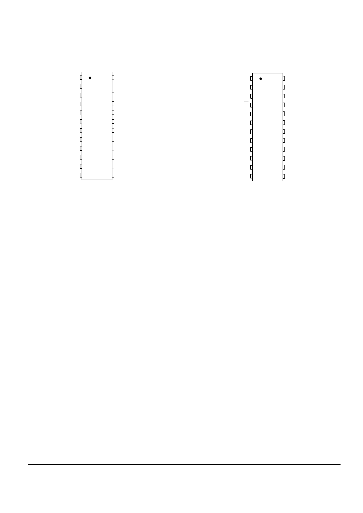
MODULATOR
B1
B1
B1
B1
B2
B2
B2
B2
D1
D1
D1
D1
D2
D2
D2
LO1
LO2
LB
SE
MSI
CCI
PD
VD
LI
V
ref
DEMODULATOR
SEQUENCE
AND
CONTROL
8 8 2 2
8
8
2
2
B CHANNEL BUFFERS
B CHANNEL BUFFERS
D CHANNEL BUFFERS
7
6
20
21
19
10
8
18
13
15
14
D2I
D1I
RE2
Rx
RE1
D2O
D1O
TDC/RDC
Tx
TE1
TE2
D CHANNEL BUFFERS
+
–
DCLK
9
D2
MC145421 MASTER ISDN BLOCK DIAGRAM
B1
B1
B1
B1
B2
B2
B2
B2
D1
D1
D1
D1
D2
D2
D2
D2
LO1
LO2
CCI
LB
PD
VD
LI
V
ref
XTL
Mu/A
TONE
23
22
17
18
4
11
16
19
5
3
2
MODULATOR
OSC
DEMODULATOR
SEQUENCE
AND
CONTROL
8 8 2 2
2
2
÷
2
8
8
B CHANNEL BUFFERS
B CHANNEL BUFFERS
D CHANNEL BUFFERS
D CHANNEL BUFFERS
7
6
10
8
9
20
13
15
14
21
D2I
D1I
Rx
D2O
DCLK
D1O
Tx
BCLK
EN1
EN2
+
–
12
CLKOUT
MC145425 SLAVE ISDN BLOCK DIAGRAM
MC145421•MC145425 MOTOROLA
4
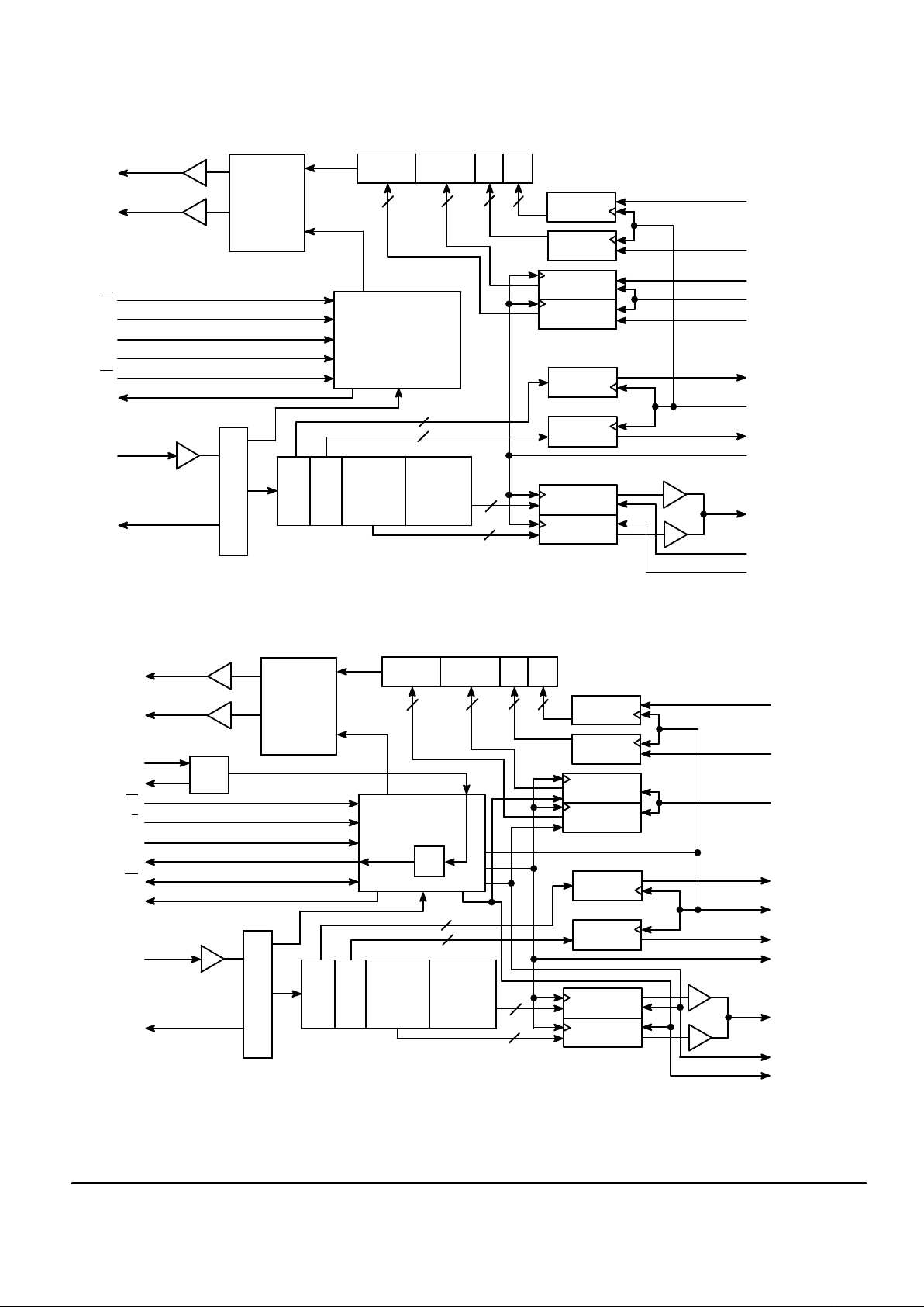
ABSOLUTE MAXIMUM RATINGS (Voltage Referenced to V
SS
)
Rating
Symbol Value Unit
DC Supply Voltage VDD – V
SS
– 0.5 to 6.5 V
Voltage Any Pin to V
SS
V – 0.5 to VDD + 0.5 V
DC Current, Any Pin (Excluding VDD,
VSS)
I ± 10 mA
Operating Temperature T
A
– 40 to + 85 °C
Storage Temperature T
stg
– 85 to + 150 °C
RECOMMENDED OPERATING CONDITIONS (T
A
= – 40 to + 85°C)
Parameter
Pins Min Typ Max Unit
DC Supply Voltage V
DD
4.5 5.0 5.5 V
Frame Rate MC145421 (See Note) MSI — 8.0 — kHz
MC145421/25 Frame Slip Rate (See Note) — — — 0.25 %
CCI Clock Frequency — — 8.192 8.29 MHz
TDC/RDC Data Clocks (for Master) — 0.128 — 4.1 MHz
DCLK — 0.016 — 4.1 MHz
Modulation Baud Rate (CCI/16) LO1, LO2 — 512 — kHz
NOTE: The slave’s crystal frequency divided by 1024 must equal the master’s MSI frequency ± 0.25% for optimum operation. Also, the
8.192 MHz input at the master divided by 1024 must be within 0.048% of the master’s 8 kHz MSI clock frequency.
DIGITAL CHARACTERISTICS (V
DD
= 5 V, TA = – 40 to + 85°C)
Parameter
Min Max Unit
Input High Level 3.5 — V
Input Low Level — 1.5 V
Input Current, V
DD
— 15 mA
Input Current (Digital Pins) — 5 µA
Input Capacitance — 10 pF
Output High Current (Except Tx on Master and Slave, and PD on the Slave) VOH = 2.5
VOH = 4.6
– 1.7
– 0.36
—
—
mA
Tx Output High Current VOH = 2.5
VOH = 4.6
– 3.4
– 0.7
—
—
mA
PD (Slave) Output High Current (See Note) VOH = 2.5 — – 90 µA
Output Low Current (Except Tx on Master and Slave, and PD on Slave) VOL = 0.4
VOL = 0.8
0.36
0.8
—
—
mA
Tx Output Low Current VOL = 0.4
VOL = 0.8
1.7
3.5
—
—
mA
PD (Slave) Output Low Current (See Note) VOL = 0.4 30 60 µA
Tx Three–State Impedance 100 — kΩ
XTL Output High Current VOH = 4.6 — – 450 µA
XTL Output Low Current VOH = 0.4 450 — µA
NOTE: To overdrive PD from a low level to 3.5 V, or a high level to 1.5 V requires a minimum of ± 800 µA drive capability.
ANALOG CHARACTERISTICS (V
DD
= 5 V, TA = 0 to 70°C)
Parameter
Min Max Unit
Modulation Differential Amplitude RL = 880 Ω (LO1 – LO2) 4.6 — Vpeak
Modulation Differential DC Offset — 40 mV
V
ref
Voltage (Typically 9/20 S (VDD – VSS))
2.0 2.5 V
PCM Tone Level – 22 – 18 dBm
Demodulator Input Amplitude 50 — mVpeak
Demodulator Input Impedance (LI to V
ref
) 75 300 kΩ
This device contains circuitry to protect the
inputs against damage due to high static
voltages or electric fields; however, it is
advised that normal precautions be taken to
avoid applications of any voltage higher than
maximum rated voltages to this high impedance circuit. For proper operation it is recommended that Vin and V
out
be constrained to
the range VSS ≤ (Vin or V
out
) ≤ VDD. Reliability
of operation is enhanced if unused inputs are
tied to an appropriate logic voltage level (e.g.,
either VSS or VDD).

MC145421•MC145425MOTOROLA
5
MC145421 MASTER PIN DESCRIPTIONS
V
DD
Positive Supply (Pin 24)
The most positive power supply pin, normally + 5 V with
respect to VSS.
V
SS
Negative Supply (Pin 1)
The most negative supply pin and logic ground, normally
0 V.
V
ref
Reference Output (Analog Ground) (Pin 2)
This pin is the output of the internal reference supply and
should be bypassed to VDD and VSS with 0.1 µF capacitors.
This pin usually serves as an analog ground reference for
transformer coupling of the device’s incoming bursts from the
line. No external dc load should be placed on this pin.
LI
Line Input (Pin 3)
This pin is an input to the demodulator for the incoming
bursts. The input has an internal 240 k
Ω resistor tied to the
V
ref
pin, so an external capacitor or line transformer may be
used to couple the input signal to the device with no dc offset.
LO1, LO2
Line Driver Outputs (Pins 23, 22)
These push–pull outputs drive the twisted pair transmission line with a 512 kHz modified DPSK (MDPSK) burst each
125 µs, in other words at an 8 kHz rate. When not modulating
the line, these pins are driven to the active high state —
being the s ame potential, they create a n ac short. When
used in conjunction with feed resistors, proper line termination is maintained.
SE
Signal Enable Input (Pin 11)
At the time of a negative transition on this pin, an internal
latch stores the states of LB
and PD for as long as SE is held
low. During this time, the VD, DO1, and DO2 outputs are
driven to the high–impedance state. When SE is high, all
pins function normally.
LB
Loopback Control (Pin 4)
A low level on this pin ties the internal modulator output to
the internal demodulator input, which loops the entire burst
for testing purposes. During the loopback operation, the LI
input is ignored and the LO1 and LO2 drivers are driven to
the active high level. The state of this pin is internally latched
if the SE pin is held low. This feature is only active when the
PD
input is high.
PD
Power–Down Input (Pin 12)
When held low the ISDN UDLT powers down, except the
circuitry that is necessary to demodulate an incoming burst
and to output VD, B, and D channel data bits. When PD is
brought high, the ISDN UDLT powers up. Then, it begins
transmitting every MSI period to the slave device, shortly
after the rising edge of MSI. The state of this pin is latched if
the SE pin is held low.
VD
Valid Data Output (Pin 5)
A high level on this pin indicates that a valid line transmission has been demodulated. A valid transmission burst is
determined by proper synchronization and the absence of
detected bit errors. VD changes state on the rising edge of
MSI when PD
is high. When PD is low, VD changes state at
the end of demodulation of a transmission burst and does not
change again until three MSI rising edges have occurred, at
which time it goes low, or until the next demodulation of a
burst. VD is a standard B–series CMOS output and is high
impedance when SE is low.
MSI
Master Sync Input (Pin 16)
This pin is the master, 8 kHz frame reference input. The
rising edge of MSI loads B and D channel data which had
been input during the previous frame into the modulator section of the device and initiates the outbound burst onto the
twisted–pair cable. The rising edge of MSI also initiates the
buffering of the B and D channel data demodulated during
the previous frame. MSI should be approximately leading
edge aligned with the TDC/RDC data clock input pin.
CCI
High–Speed Clock Input (Pin 17)
An 8.192 MHz clock should be supplied to this input. The
8.192 MHz input should be 50% duty cycle. However, it may
free–run with respect to all other clocks without performance
degradation.
D1I, D2I
D Channel Signaling Bit Inputs (Pins 6, 7)
These inputs are 16 kbps serial data inputs. Two bits
should be clocked into each of these inputs between the rising edges of the MSI frame reference clock. The first bit of
each D channel is clocked into an intermediate buffer on the
first falling edge of the DCLK following the rising edge of MSI.
The second bit of each D channel is clocked in on the next
negative transition of the DCLK. If further DCLK negative
edges occur, new information is serially clocked into the buffer replacing the previous data one bit at a t ime. Buffered
D channel data bits are burst to the slave device on the next
rising edge of the MSI frame reference clock.
D1O, D2O
D Channel Signal Outputs (Pins 9, 10)
These serial outputs provide the 16 kbps D channel signaling information from the incoming burst. T wo data bits should
be clocked out of each of these outputs between the rising
edges of the MSI frame reference clock. The rising edge of
MSI produces the first bit of each D channel on its respective
pin. Circuitry then searches for a negative D channel clock
edge. This tells the D channel data shift register to produce
the second D channel b it on the next rising e dge of the
DCLK. Further positive edges of the DCLK recirculate the
D channel output buffer information.

MC145421•MC145425 MOTOROLA
6
DCLK
D Channel Clock Input (Pin 8)
This input is the transmit and receive data clock for both
D channels. D channel i nput and output operation is described in the D1O, D2O pin description.
Tx
Transmit Data Output (Pin 13)
This pin is high impedance when both TE1 and TE2 are
low. This pin serves as an output for B channel information
received from the slave device. The B channel data is under
the control of TE1, TE2, and TDC/RDC. (See TE1, TE2
description.)
Rx
Receive Data Input (Pin 21)
B channel data is input on this pin and is controlled by the
RE1, RE2, and TDC/RDC pins. (See RE1, RE2 description.)
TE1, TE2
Transmit Data Enable Input (Pins 14, 15)
These two pins control the output of data for their respective B channel on the Tx output pin. When both TE1 and TE2
are low, the Tx pin is high impedance. The rising edge of the
respective enable p roduces the first bit of t he selected
B channel data on the Tx pin. Internal circuitry then scans for
the next negative transition of the TDC/RDC clock. Following
this event, the next seven bits of the selected B channel data
are output on the next seven rising edges of the TDC/RDC
data clock. When TE1 and TE2 are high simultaneously , data
on the Tx pin is undefined. TE1 and TE2 should be approximately leading–edge aligned with the TDC/RDC data clock
signal. In order to keep the Tx pin out of the high–impedance
state, these enable lines should be high while the respective
B channel data is being output.
RE1, RE2
Receive Data Enable Inputs (Pins 19, 20)
These inputs control the input of B channel data on the Rx
pin of the device. The rising edge of the respective enable
signal causes the device to load the selected receive data
buffer with d ata from the Rx pin on the next eight falling
edges o f the TDC/RDC clock input. The RE1 and RE2
enables should be roughly leading–edge aligned with the
TDC/RDC data clock input. These enables are rising edge
sensitive and need not be high for the entire B channel input
period.
TDC/RDC
Transmit/Receive Data Clock Input (Pin 18)
This input is the transmit and receive data clock for the
B channel data. As described in the TE1/TE2 and the RE1/
RE2 sections, output data changes state on the rising edge
of this signal, and input data is read on the falling edges of
this s ignal. T DC/RDC should be r oughly l eading–edge
aligned with the TE1, TE2, RE1, and RE2 enables, as well as
the MSI frame reference signal.
MC145425 SLAVE PIN DESCRIPTIONS
V
DD
Positive Supply (Pin 24)
The most positive power supply pin, normally + 5 V with
respect to VSS.
V
SS
Negative Supply (Pin 1)
The most negative supply pin and logic ground, normally
0 V.
V
ref
Reference Output (Analog Ground) (Pin 2)
This pin is the output of the internal reference supply and
should be bypassed to VDD and VSS with 0.1 µF capacitors.
This pin usually serves as an analog ground reference for
transformer coupling of the device’s incoming bursts from the
line. No external dc load should be placed on this pin.
LI
Line Input (Pin 3)
This pin is an input to the demodulator for the incoming
bursts. The input has an internal 240 kΩ resistor tied to the
V
ref
pin, an external capacitor or line transformer may be
used to couple the input signal to the device with no dc offset.
LO1, LO2
Line Driver Outputs (Pins 23, 22)
These push–pull outputs drive the twisted pair transmission line with a 512 kHz modified DPSK (MDPSK) burst each
125 µs; in other words at an 8 kHz frame rate. When not
modulating the line, these pins are driven to the active high
state — being the same potential, they create an ac short.
When used in conjunction with feed resistors, proper line termination is maintained.
CLK OUT
Clock Output (Pin 19)
This pin serves as a buffered output of the crystal f requency divided by two. This clock is provided for systems
using the MC145428 Data Set Interface asynchronous/synchronous terminal adaptor device.
LB
Loopback Control Input (Pin 4)
When this pin is low, the incoming B channels from the
master are burst back to the master — instead of the Rx B
channel input data. The B channel data from the master continues to be output at the slave’s Tx pin during loopback. If
the TONE and the loopback function are active simultaneously, the loopback function overrides the TONE function.
D channel data is not affected by LB
.
VD
Valid Data Output (Pin 5)
A high on this pin indicates that a valid transmission burst
has been demodulated. A valid burst is determined by proper
synchronization and the absence of detected bit errors. If no
transmissions from the master have been received in the last
250 µs, as determined by an internal oscillator, VD will go
low.

MC145421•MC145425MOTOROLA
7
Mu/A
Tone Format Input (Pin 11)
This pin determines the PCM code for the 500 Hz square
wave tone generated when the TONE input is high — Mu–
Law (Mu/A = 1) or CCITT A–Law (Mu/A = 0) format.
TONE
Tone Enable Input (Pin 16)
A high on this pin causes a 500 Hz square wave PCM tone
to be inserted in place of the demodulated B channel data on
B channel 1. This feature allows the designer to provide
audio feedback for telset keyboard operations.
PD
Power Down Input/Output (Pin 12)
This is a bidirectional pin with a weak output driver so that
it can be externally overdriven. When h eld low, the ISDN
UDLT is powered down, and the only active circuitry is that
which is necessary for demodulation, generation of EN1,
EN2, BCLK, and DCLK, and outputting of the data bits and
VD. When held high, the ISDN UDLT is powered up and
transmits normally in response to received bursts from the
master. If the ISDN UDLT is powered up for 250 µs — which
is derived from an internal oscillator and no bursts from the
master have occurred — the I SDN s lave U DLT generates
a free–running s et of EN1, EN2, BCLK, and DCLK signals
and sends a burst to the master device every other 125 µs
frame. This is a wake–up signal to the master.
When PD
is floating and a burst from the master is demod-
ulated, the weak output drivers will try to force PD
high. It will
try to force PD
low if 250 µs have elapsed without a burst
from the master being successfully demodulated. This allows
the slave d evice to self power up and down in demand–
powered loop systems.
CCI
Crystal Input (Pin 17)
Normally, an 8.192 MHz crystal is tied between this pin
and the XTL pin. A 10 MΩ resistor between CCI and XTL and
25 pF capacitors from CCI and XTL to VSS are required to
ensure stability and start–up. CCI may also be driven with an
external 8.192 MHz signal if a crystal is not desired.
XTL
Crystal Output (Pin 18)
This pin is capable of driving one external CMOS input and
15 pF of additional load capacitance.
D1I, D2I
D Channel Inputs (Pins 6, 7)
These two pins are inputs for the 16 kbps D data channels.
The D channel data bits are clocked in serially on the negative edge of the 16 kbps DCLK output pin.
D1O, D2O
D Channel Outputs (Pins 9, 10)
These two pins are outputs for the 16 kbps D data channels. These pins are updated on the rising edges of the slave
DCLK output pin.
Tx
Transmit Data Output (Pin 13)
This line is an output for the B channel data received from
the master. B channel 1 data is output on the first eight cycles
of the BCLK output when EN1 is high. B channel 2 data is
output on the next eight cycles of the BCLK, when EN2 is
high. B channel data bits are clocked out on the rising edge
of the BCLK output pin.
DCLK
D Channel Clock Output (Pin 8)
This output is the transmit and receive data clock for both
D channels. It starts upon demodulation of a burst from the
master device. This signal is rising e dge aligned with the
EN1 and BCLK signals. After the demodulation of a burst,
the DCLK line completes two cycles and then remains low
until another burst from the master is demodulated. In this
manner synchronization with the master is established and
any clock slip between master and slave is absorbed each
frame.
Rx
Receive Data Input (Pin 21)
This pin is an input for the B channel data. B channel 1
data is clocked in on the first eight falling edges of the BCLK
output following the rising edge of the EN1 output. B channel
2 data is clocked in on the next eight falling edges of the
BCLK following the rising edge of the EN2 output.
EN1
B Channel 1 Enable Output (Pin 15)
This line is an 8 kHz enable signal for the input and output
of the B channel 1 data. While EN1 is high, B channel 1 data
is clocked out on the Tx pin on the first eight rising edges of
the BCLK. During this same time, B channel 1 input data is
clocked in on the Rx pin on the first eight falling edges of the
BCLK. The VD pin is also updated on the rising edge of the
EN1 signal. EN1 serves as the slave device’s 8 kHz frame
reference signal.
EN2
B Channel 2 Enable Output (Pin 14)
This pin is the logical inverse of the EN1 output and is used
to signal the time slot for the input and output of data for the
B channel 2 data.
BCLK
B Channel Data Clock Output (Pin 20)
This is a standard B series output which provides the data
clock for the B channel data. This clock signal is 128 kHz and
begins operating upon the successful demodulation o f a
burst from the master. At this time, EN1 goes high and BCLK
starts toggling. BCLK remains active for 16 periods, at the
end of which time it remains low until another burst is received from the master. In this manner synchronization between the master and slave is established and any clock
slippage is absorbed each frame.

MC145421•MC145425 MOTOROLA
8
BACKGROUND
The MC145421 and the MC145425 ISDN UDLTs provide
an economical means of sending and receiving two B channels ( 64 kbps each) o f voice/data and two D c hannels
(16 kbps each) of signal data in a two–wire configuration at
distances up to one kilometer. There are two ISDN UDLTs,
master and slave. The master UDL T is compatible with existing and evolving PABX architectures. This device transmits
2B+2D channels of data to the remote slave. At the remote
end, the slave device presents a replica of the PBX backplane to the terminal devices.
These devices permit existing digital PBX architectures to
remain unchanged and provide enhanced voice/data communication services throughout the PBX service area by simply replacing a subscriber’s line card and telset.
All operations occur within the boundaries of an 8 kHz
frame (125 µs). In the master, the frame sequence begins on
the rising edge of MSI. In the slave, the frame begins after
the demodulation of a burst from the master. The slave initializes its timing controls at this point to stay synchronized with
the master.
During one 125 µs frame f our main a ctivities are performed:
1. Previously buffered 2B+2D channel data is burst to the
other end.
2. New 2B+2D channel data is accepted for the next
frame’s transmission.
3. An incoming burst is demodulated and stored.
4. 2B+2D channel data from the previous demodulated
frame is output.
The bursts are 20 bits long, composed of two 8–bit B channels and two 2–bit D channels. Bursts are encoded using a
modified DPSK method at 512 kHz. Since a single wire pair
is used, half–duplex operation is used. A 512 kHz burst is
sent from end to end in a ping–pong fashion. This method
provides apparent full–duplex 160 kbps transmission of data
at distances up to one kilometer.
GENERAL
The ISDN UDLT consists of a modulator, a demodulator,
intermediate data registers, receive and transmit data registers, and sequencing and control logic. The Rx and Tx buffers interface digitally to the line card backplane signals, while
the modulator and demodulator interface to the twisted pair
transmission media. Intermediate data registers buffer data
between these main components. The ISDN UDLT is intended to operate with a 5 V power supply and can be driven
by CMOS or TTL logic.
MASTER OPERATION
In the master, the rising edge of MSI initiates the 125 µs
frame. B channel data is clocked into the Rx registers under
control of TDC/RDC, RE1, and RE2. This data is combined
with the D channel data clocked in on pins D1I and D2I by the
DCLK. The resulting 20–bit packet is stored for the next
frame transmission to the slave UDLT.
The burst output to the slave consists of the 2B+2D data
loaded during the previous frame. The burst received from
the slave is demodulated and stored for outputting in the following frame.
B channel bits demodulated in the previous frame are output on the Tx pin under control of TDC/RDC, TE1, and TE2.
Demodulated D channel bits are output on the D1O and D2O
output pins. The indication of a valid burst demodulation is
the VD output, which is updated at the start of every frame.
SLAVE OPERATION
In normal slave operation, the main synchronizing event is
completion of demodulating a burst from the master UDLT.
This action initializes the 125 µs frame boundary of the slave.
During the slave frame, B channel data is loaded and stored
under control of the BCLK, EN1, and EN2 outputs. D channel
data is loaded at D1I and D21 under control of the DCLK
output.
The demodulated burst from the master is separated into
its D channel and B channel components and output on the
D1O, D2O, and Tx pins. The return burst to the master consisting of previously loaded 2B+2D data is transmitted eight
bauds after the completion of demodulation of the master’s
burst. This provides a period for line transients to diminish.
The start of the slave frame initiates two cycles of the
16 kHz DCLK, and one cycle each of the 8 kHz EN1 and EN2
enables. After completing their cycles, these outputs remain
low until another demodulation signals the start of a new
slave frame. In this manner, clock slip between the master
and slave UDLTs is absorbed each frame.
POWER–DOWN OPERATION
When PD
is low in the master, the ISDN UDLT is powered
down and only that circuitry necessary to demodulate incoming bursts is active. No transmissions to the slave occur
during power down. If the master is receiving bursts from the
slave, the VD pin will change state upon completion of the
demodulation.
When the PD
input pin is driven high, the master ISDN
UDLT is powered up. In this mode, the master bursts to the
slave every frame. B and D channel data can be loaded and
unloaded and VD is updated on the MSI rising edge.
If no bursts are received by the master, whether powered
up or not, the B channel data is unknown and the D channel
bits will remain at their last known values.
The PD
pin on the slave UDLT is bidirectional with a weak
output driver that can be overdriven externally. When low,
either externally or internally derived, the slave is powered
down. No bursts to the master can be transmitted. EN1, EN2,
BCLK, and DCLK outputs are inactive during power down
except when TONE is high or a burst has been received from
the master. B and D channel data can be loaded and unloaded, and VD is updated upon completion of demodulation
of an incoming burst from the master. Input B and D channel
data is not transmitted until the slave is powered up, in which
case the first burst contains the most recently loaded data.
When the PD
pin is high, the slave is powered up and
transmits every frame, the data enables and clocks are output, and data can be loaded and unloaded.
TIME–OUT OPERATION
Time–out is an operating state in both the UDLT master
and slave devices. This state indicates that no incoming
bursts have been demodulated, forcing the VD pin low. An
internal counter is incremented for each frame that does not
contain an incoming burst. The counter i s reset upon demodulating a burst from the far end. Time–out can occur
whether the device is powered up or down.

MC145421•MC145425MOTOROLA
9
In the master, time–out begins on the rising edge of the
third MSI following the last received burst. This is equivalent
to two MSI frames. The VD output is forced low during time–
out. The B channel output data will be unknown, but the
D channel bits will remain at their last values. Successful demodulation of a burst from the slave will result in leaving the
time–out state on the next rising MSI edge.
When the PD
pin is used as an output on the slave UDLT,
time–out controls the pin. Time–out forces the PD
output low
to indicate that the device has powered itself down. In this
case, the slave will not transmit to the master. However,
when a valid burst is received, time–out ends and the PD
pin
is driven high to indicate power up. This feature allows the
slave UDLT to self–power–up and down in demand–powered
loop systems.
NOTE
The slave uses a free running clock during time–
out. After a long period without a burst from the
master, the timing between master and slave
could be such that more than one burst will be
needed to resync the two devices.
125 µs
1ST BIT 2ND BIT
1ST BIT 2ND BIT
B CHANNEL 1 OUTPUT B CHANNEL 2 OUTPUT
B CHANNEL 2 INPUTB CHANNEL 1 INPUT
HIGH–Z
MSI
VD
DCLK
D1I, D2I
D1O, D2O
TDC/RDC
TE1
TE2
RE1
RE2
Tx
Rx
DON’T CARE
Figure 1. Typical MC145421 Master ISDN UDLT Timing

MC145421•MC145425 MOTOROLA
10
125 µs
1ST BIT
1ST BIT
2ND BIT
2ND BIT
B CHANNEL 1 OUTPUT B CHANNEL 2 OUTPUT
B CHANNEL 1 INPUT B CHANNEL 2 INPUT
SLIP
ABSORBED
1 8 9 16
EN1
EN2
DCLK
VD
D1I, D2I
D1O, D2O
Tx
Rx
BCLK
Figure 2. MC145425 Slave ISDN UDLT Timing
Top Trace: MSI
Bottom Trace: Outgoing burst measured at LI (with respect to V
ref
)
Figure 3. Master Burst

MC145421•MC145425MOTOROLA
11
110
Ω
110
Ω
110
Ω
110
Ω
+ 5 V
+ 5 V
+ 5 V
5 k
Ω
10 k
Ω
L2
L1
TWISTED PAIR WIRE
LO1
LO2
V
ref
LI
MASTER
OR
SLAVE
ISDN UDLT
+ 5 V
0.1
µ
F
0.1
µ
F
Rx
Tx
INDUCTANCE OF Tx: WINDING: 1.75 mH
TURNS RATIO: Tx L1 + L2 2:1
TURNS RATIO: Rx L1 + L2 4:1
DIODES: 1N4148 OR EQUIVALENT
TRANSFORMER PARAMETERS
Figure 4. Interface to Twisted Pair Wire

MC145421•MC145425 MOTOROLA
12
SWITCHING CHARACTERISTICS (V
DD
= 5 V, TA = 0 to 70°C; C
Load
= 50 pF)
No.*
Parameter Min Max Unit
Master Timing
1 TDC/RDC Pulse Width High 110 — ns
2 TDC/RDC Pulse Width Low 110 — ns
3 MSI Rising Edge to TDC/RDC Falling Edge 90 — ns
4 MSI Pulse Width 200 — ns
5 MSI Rising Edge to First DCLK Falling Edge 90 — ns
6 MSI Rising Edge to First D1O, D2O Bit Valid — 100 ns
7 TE1, TE2 Rising Edge to TDC/RDC Falling Edge 110 — ns
8 TDC/RDC Falling Edge to TE1, TE2 Rising Edge 20 — ns
9 TE1, TE2 Rising Edge to First Tx Data Bit Valid — 50 ns
10 TDC/RDC Rising Edge to Tx Data Bits 2 Through 8 Valid — 50 ns
11 TE1, TE2 Falling Edge to Tx High–Impedance — 70 ns
12 REI, RE2 Rising Edge to TDC/RDC Falling Edge 110 — ns
13 TDC/RDC Falling Edge to RE1, RE2 Rising Edge 20 — ns
14 Rx Data Setup (Data Valid Before TDC/RDC Falling Edge) 50 — ns
15 Rx Data Hold (Data Valid After TDC/RDC Falling Edge) 20 — ns
16 RE1, RE2 Pulse Width 220 — ns
17 DCLK Rising Edge to D1O, D2O Bit Valid — 135 ns
18 D1I, D2I Data Setup (Data Valid Before DCLK Falling Edge) 50 — ns
19 D1I, D2I Data Hold (Data Valid After DCLK Falling Edge) 20 — ns
20 DCLK Pulse Width Low 110 — ns
21 DCLK Pulse Width High 110 — ns
22 MSI Rising Edge to VD Valid — 150 ns
23 PD, LB Setup (PD, LB Valid Before MSI Rising Edge) 50 — ns
24 PD, LB Hold (PD, LB Valid After MSI Rising Edge) 20 — ns
Slave Timing
25 BCLK Pulse Width High (CCI = 8.192 MHz) 3.66 4.15 µs
26 BCLK Pulse Width Low (CCI = 8.192 MHz) 3.66 4.15 µs
27 EN1 or EN2 Rising Edge to BCLK Rising Edge 75 175 ns
28 EN1 or EN2 Rising Edge to DCLK Rising Edge — ± 50 ns
29 EN1 or EN2 Rising Edge to First Tx Data Bit Valid — 50 ns
30 BCLK Rising Edge to Tx Data Bits 2 Through 8 Valid — – 75 ns
31 DCLK Pulse Width High (CCI = 8.192 MHz) 31.0 31.5 µs
32 DCLK Pulse Width Low (CCI = 8.192 MHz) 31.0 31.5 µs
33 DCLK Rising Edge to D1O, D2O Bits Valid — 50 ns
34 Rx Setup (Rx Data Valid Before BCLK Falling Edge) 175 — ns
35 Rx Hold (Rx Data Valid After BCLK Falling Edge) 20 — ns
36 D1I, D2I Setup (D1I, D2I Valid Before DCLK Falling Edge) 50 — ns
37 D1I, D2I Hold (D1I, D2I Valid After DCLK Falling Edge) 20 — ns
38 EN1 Rising Edge to VD Valid — 50 ns
SE Pin Timing
39 LB, PD Hold (LB, PD Valid After SE Falling Edge) 20 — ns
40 D1O, D2O, VD High Impedance After SE Falling Edge — 70 ns
41 D1O, D2O, VD Valid After SE Rising Edge 60 — ns
42 LB, PD Setup (LB, PD Valid Before SE Rising Edge) 50 — ns
*See Switching Characteristics waveforms.

MC145421•MC145425MOTOROLA
13
NOTE: All measurement thresholds are 30% or 70% of V .
DD
MSI
TDC/RDC
TE1, TE2
Tx
RE1, RE2
Rx
DCLK
D1O, D2O
D1I, D2I
VD
PD, LB
DON’T CARE
BIT 1
VALID DATA BIT
VALID
DON’T CAREDON’T CAREDON’T CARE
DON’T CAREDON’T CARE
BIT 1
BIT 2
BIT 2
87654321
4
3
1
2
11
7
8
9
10
12
13
14
155
16
176
21
20
18
23
24
22 19
87654321
MASTER SWITCHING CHARACTERISTICS

MC145421•MC145425 MOTOROLA
14
SLAVE SWITCHING CHARACTERISTICS
MASTER SE PIN TIMING
PREVIOUS STATE
INTERNALLY LATCHED
VALIDVALID
SE
LB, PD
D1O, D2O, VD
39
40
41
42
BCLK
EN1
EN2
Tx
Rx
DCLK
D1O, D2O
D1I, D2I
VD VALID
DON’T CAREBIT 2DON’T CAREDON’T CAREDON’T CARE BIT 1
BIT 1 BIT 2
26
27
28
29
30
31 32
33
34
35
36
37
38
25
28
33
27
29
87654321 87654321 1
87654321 87654321 1
Note: All measurement thresholds are 30% or 70% of V
DD
.

MC145421•MC145425MOTOROLA
15
PACKAGE DIMENSIONS
P SUFFIX
PLASTIC PACKAGE
CASE 709–02
MIN MINMAX MAX
MILLIMETERS INCHES
DIM
A
B
C
D
F
G
H
J
K
L
M
N
31.37
13.72
3.94
0.36
1.02
1.65
0.20
2.92
0
°
0.51
32.13
14.22
5.08
0.56
1.52
2.03
0.38
3.43
15
°
1.02
1.235
0.540
0.155
0.014
0.040
0.065
0.008
0.115
0
°
0.020
1.265
0.560
0.200
0.022
0.060
0.080
0.015
0.135
15
°
0.040
2.54 BSC
15.24 BSC
0.100 BSC
0.600 BSC
NOTES:
1. POSITIONAL TOLERANCE OF LEADS (D),
SHALL BE WITHIN 0.25 (0.010) AT MAXIMUM
MATERIAL CONDITION, IN RELATION TO
SEATING PLANE AND EACH OTHER.
2. DIMENSION L TO CENTER OF LEADS WHEN
FORMED PARALLEL.
3. DIMENSION B DOES NOT INCLUDE MOLD
FLASH.
1 12
1324
B
A
N
SEATING
PLANE
M
J
L
DF
GH
C
K
DW SUFFIX
SOG PACKAGE
CASE 751F–04
MIN MINMAX MAX
MILLIMETERS INCHES
DIM
A
B
C
D
F
G
J
K
M
P
R
17.80
7.40
2.35
0.35
0.41
0.23
0.13
0
°
10.05
0.25
18.05
7.60
2.65
0.49
0.90
0.32
0.29
8
°
10.55
0.75
0.701
0.292
0.093
0.014
0.016
0.009
0.005
0
°
0.395
0.010
0.711
0.299
0.104
0.019
0.035
0.013
0.011
8
°
0.415
0.029
1.27 BSC 0.050 BSC
NOTES:
1. DIMENSIONING AND TOLERANCING PER
ANSI Y14.5M, 1982.
2. CONTROLLING DIMENSION: MILLIMETER.
3. DIMENSION A AND B DO NOT INCLUDE MOLD
PROTRUSION.
4. MAXIMUM MOLD PROTRUSION 0.15
(0.006) PER SIDE.
5. DIMENSION D DOES NOT INCLUDE
DAMBAR PROTRUSION.
ALLOWABLE
DAMBAR PROTRUSION SHALL BE 0.13
(0.005) TOTAL IN EXCESS OF D
DIMENSION AT MAXIMUM MATERIAL
CONDITION.
-A-
-B-
1 14
1528
-T-
C
SEATING
PLANE
0.010 (0.25)
B
M M
M
J
-T-
K
26X G
28X D
14X P
R
X 45°
F
0.010 (0.25) T A B
M
S S

MC145421•MC145425 MOTOROLA
16
Motorola reserves the right to make changes without further notice to any products herein. Motorola makes no warranty , representation or guarantee regarding
the suitability of its products for any particular purpose, nor does Motorola assume any liability arising out of the application or use of any product or circuit,
and specifically disclaims any and all liability, including without limitation consequential or incidental damages. “T ypical” parameters can and do vary in different
applications. All operating parameters, including “T ypicals” must be validated for each customer application by customer’s technical experts. Motorola does
not convey any license under its patent rights nor the rights of others. Motorola products are not designed, intended, or authorized for use as components in
systems intended for surgical implant into the body, or other applications intended to support or sustain life, or for any other application in which the failure of
the Motorola product could create a situation where personal injury or death may occur. Should Buyer purchase or use Motorola products for any such
unintended or unauthorized application, Buyer shall indemnify and hold Motorola and its officers, employees, subsidiaries, affiliates, and distributors harmless
against all claims, costs, damages, and expenses, and reasonable attorney fees arising out of, directly or indirectly, any claim of personal injury or death
associated with such unintended or unauthorized use, even if such claim alleges that Motorola was negligent regarding the design or manufacture of the part.
Motorola and are registered trademarks of Motorola, Inc. Motorola, Inc. is an Equal Opportunity/Affirmative Action Employer.
How to reach us:
USA/EUROPE: Motorola Literature Distribution; JAPAN: Nippon Motorola Ltd.; Tatsumi–SPD–JLDC, Toshikatsu Otsuki,
P.O. Box 20912; Phoenix, Arizona 85036. 1–800–441–2447 6F Seibu–Butsuryu–Center, 3–14–2 Tatsumi Koto–Ku, Tokyo 135, Japan. 03–3521–8315
MFAX: RMFAX0@email.sps.mot.com – TOUCHTONE (602) 244–6609 HONG KONG: Motorola Semiconductors H.K. Ltd.; 8B Tai Ping Industrial Park,
INTERNET: http://Design–NET.com 51 Ting Kok Road, Tai Po, N.T., Hong Kong. 852–26629298
MC145421/D
*MC145421/D*
◊
 Loading...