

SEMICONDUCTOR TECHNICAL DATA
Order this document
by MC145422/D
The MC145422 and MC145426 UDLTs are high–speed data transceivers
that provide 80 kbps full–duplex data communication over 26 AWG and larger
twisted–pair cable up to two kilometers in distance. Intended primarily for use in
digital subscriber voice/data telephone systems, these devices can also be
used in remote data acquisition and control systems. These devices utilize a
256 kilobaud modified differential phase shift keying burst modulation technique
for transmission to minimize RFI/
distribution and duplex data communication can be obtained using a single
twisted–pair wire.
These devices are designed for compatibility with existing, as well as
evolving, telephone switching hardware and software architectures.
The UDLT chip–set consists of the MC145422 Master UDLT for use at the
telephone switch linecard and the MC145426 Slave UDL T for use at the remote
digital telset and/or data terminal.
The devices employ CMOS technology in order to take advantage of their
reliable low–power operation and proven capability for complex analog/digital
LSI functions.
• Provides Full–Duplex Synchronous 64 kpbs Voice/Data Channel and Two
8 kbps Signaling Data Channels Over One 26 AWG Wire Pair Up to Two
Kilometers
• Compatible with Existing and Evolving Telephone Switch Architectures and
Call Signaling Schemes
• Automatic Detection Threshold Adjustment for Optimum Performance Over
V arying Signal Attenuations
• Protocol Independent
• Single 5 V Power Supply
• 22–Pin PDIP, 24–Pin SOG Packages
• Application Notes AN943, AN949, AN968, AN946, and AN948
MC145422 Master UDL T
• Pin Controlled Power–Down and Loopback Features
• Signaling and Control I/O Capable of Sharing Common Bus Wiring with
Other UDLTs
• V ariable Data Clock — 64 kHz to 2.56 MHz
• Pin Controlled Insertion/Extraction of 8 kbps Channel into LSB of 64 kbps
Channel for Simultaneous Routing of Voice and Data Through PCM Voice
Path of Telephone Switch
MC145426 Slave UDL T
• Compatible with MC145500 Series PCM Codec–Filters
• Pin Controlled Loopback Feature
• Automatic Power–Up/Power–Down Feature
• On–Chip Data Clock Recovery and Generation
• Pin Controlled 500 Hz D3 or CCITT Format PCM Tone Generator for
Audible Feedback Applications
EMI and crosstalk. Simultaneous power
P SUFFIX
22
1
24
1
ORDERING INFORMATION
MC145422P Plastic DIP
MC145426P Plastic DIP
MC145422DW SOG Package
MC145426DW SOG Package
PLASTIC DIP
CASE 708
DW SUFFIX
SOG PACKAGE
CASE 751E
REV 2
9/95
Motorola, Inc. 1995
MC145422•MC145426MOTOROLA
1
PIN ASSIGNMENTS
MC145422 — MASTER
(PLASTIC PACKAGE)
1
V
SS
V
ref
LI
LB
VD
SI1
SO1
SI2
SO2
SE
PD
2
3
4
5
6
7
8
9
10
11
22
21
20
19
18
17
16
15
14
13
12
V
DD
LO1
LO2
RE1
Rx
TDC/RDC
CCI
Tx
TE1
SIE
MSI
MC145426 — SLA VE
(PLASTIC PACKAGE)
1
V
SS
V
ref
LI
LB
VD
SI1
SO1
SI2
SO2
Mu/A
PD
2
3
4
5
6
7
8
9
10
11
22
21
20
19
18
17
16
15
14
13
12
V
DD
LO1
LO2
RE1
Rx
CLK
X2
X1
Tx
TE1
TE
NC = NO CONNECTION
MC145422 — MASTER
(SOG PACKAGE)
1
V
SS
2
V
ref
3
LI
4
NC NC
5
LB
VD
6
7
SI1
SO1
8
SI2
9
10
SO2
SE
11
PD
12
24
23
22
21
20
19
18
17
16
15
14
13
V
DD
LO1
LO2
RE1
Rx
TDC/RDC
CCI
Tx
TE1
SIE
MSI
MC145426 — SLA VE
(SOG PACKAGE)
1
V
SS
2
V
ref
3
LI
421NC NC
LB
5
VD
6
SI1
7
8
SO1
9
SI2
10
SO2
11
Mu/A
PD
12
24
23
22
20
19
18
17
16
15
14
13
V
DD
LO1
LO2
RE1
Rx
CLK
X2
X1
Tx
TE1
TE
MC145422•MC145426 MOTOROLA
2
MC145422 MASTER UDLT BLOCK DIAGRAM
LO1
LO2
CCI
MSI
LI
*— SE controlled latch
+ 1
– 1
MODULA TION BUFFER
MODULATOR
RECEIVE
REGISTER
*
SI1
SI2
SE
RE1
Rx
LB
*
PD
SIE
DIVIDE
SEQUENCE
AND
CONTROL
*
*
VD CONTROL
DEMODULATOR
DEMODULA TION BUFFER
TRANSMIT
REGISTER
*
VD
SO1
SO2
Tx
TE1
TDC/RDC
LO1
LO2
LB
TE
PD
X2
X1
LI
+ 1
– 1
POWER–
DOWN
CONTROL
OSC
MC145426 SLAVE UDLT BLOCK DIAGRAM
MODULA TION BUFFER
LOOPBACK
MODULATOR
CONTROL
SEQUENCE
CONTROL
VD CONTROL
DEMODULATOR
DEMODULA TION BUFFER
TRANSMIT
TONE
GEN.
AND
RECEIVE
REGISTER
*
SI1
SI2
Rx
RE1
Mu/A
CLK
VD
SO1
SO2
Tx
REGISTER
TE1
MC145422•MC145426MOTOROLA
3
ABSOLUTE MAXIMUM RATINGS (Voltage Referenced to V
Rating
DC Supply Voltage VDD – V
Voltage, Any Pin to V
DC Current, Any Pin (Excluding VDD,
VSS)
Operating Temperature T
Storage Temperature T
SS
RECOMMENDED OPERATING CONDITIONS (T
Parameter
DC Supply Voltage V
Power Dissipation (PD = VDD, VDD = 5 V) V
Power Dissipation (PD = VSS, TE = VSS) V
MC145422 Frame Rate MSI 7.9 8.1 kHz
MC145422 — MC145426 Frame Rate Slip (See Note 1) — — 0.25 %
CCI Clock Frequency (MSI = 8 kHz) CCI — 2.048 MHz
Data Clock Rate MC145422 TDC, RDC 64 2560 kHz
Modulation Baud Rate (See Note 2) LO1, LO2 — 256 kHz
NOTES:
1. The MC145426 crystal frequency divided by 512 must equal the MC145422 MSI Frequency ± 0.25% for optimum operation.
2. Assumes crystal frequency of 4.096 MHz for the MC145426 and 2.048 MHz CCI for the MC145422.
Symbol Value Unit
SS
V – 0.5 to VDD + 0.5 V
I ± 10 mA
A
stg
= 0 to 70°C)
A
)
SS
– 0.5 to + 9.0 V
– 40 to + 85 °C
– 85 to + 150 °C
This device contains circuitry to protect the
inputs against damage due to high static
voltages or electric fields; however, it is
advised that normal precautions be taken to
avoid applications of any voltage higher than
maximum rated voltages to this high impedance circuit. For proper operation it is recommended that Vin and V
the range VSS ≤ (Vin or V
Reliability of operation is enhanced if unused
inputs are tied to an appropriate logic voltage
level (e.g., either VSS or VDD).
Pins Min Max Unit
DD
DD
DD
4.5 5.5 V
— 80 mW
— 75 mW
be constrained to
out
) ≤ VDD.
out
DIGITAL CHARACTERISTICS (V
Input High Level 3.5 — V
Input Low Level — 1.5 V
Input Current Except LI
Input Capacitance — 7.5 pF
Output High Current (Except Tx on MC145422 VOH = 2.5 V
and Tx and PD
Output Low Current (Except Tx on MC145422 VOL = 0.4 V
and Tx and PD
PD Output High Current (MC145426) (See Note 1) VOH = 2.5 V
PD Output Low Current (MC145426) (See Note 1) VOL = 0.4 V
Tx Output High Current VOH = 2.5 V
Tx Output Low Current VOL = 0.4 V
Tx Input Impedance (TE1 = VSS, MC145422) 100 — kΩ
Crystal Frequency (MC145426, Note 2) 4.0 4.4 MHz
PCM Tone (TE = VDD, MC145426) – 22 – 18 dBm0
Three–State Current (SO1, SO2, VD, Tx on MC145422, Tx on MC145426) — ± 1 µA
V
Voltage (See Note 3) 2 3 V
ref
X2 — Oscillator Output High Drive Current (MC145426) (See Note 4) VOH = 4.6 V – 450 — µA
X2 — Oscillator Output Low Drive Current (MC145426) (See Note 4) VOL = 0.4 V 450 — µA
NOTES:
1. To overdrive PD
2. The MC145426 crystal frequency divided by 512 must equal the MC145422 MSI frequency ± 0.25% for optimum performance.
3. V
ref
4. Output drive when X1 is being driven from an external clock.
on MC145426) VOH = 4.6 V
on MC145426) VOL = 0.8 V
from a low level to 3.5 V or a high level to 1.5 V requires a minimum of ± 800 µA drive capability.
typically (9/20 VDD – VSS).
= 5 V, TA = 0 to 70°C)
DD
Parameter
VOH = 4.6 V
VOL = 0.8 V
VOH = 4.6 V
VOL = 0.8 V
Min Max Unit
LI
– 1.0
– 100
– 1.7
– 0.36
0.36
0.8
– 90
– 10
60
100
– 3.4
– 0.7
1.7
3.5
1.0
100
—
—
—
—
—
—
—
—
—
—
—
—
mA
mA
mA
mA
µA
µA
µA
MC145422•MC145426 MOTOROLA
4
ANALOG CHARACTERISTICS (V
Modulation Differential Amplitude (RL = 440 Ω) LO1 to LO2 4.5 6.0 V p–p
Modulation Differential DC Offset 0 300 mV
Demodulator Input Amplitude (See Note) 0.050 2.5 V peak
Demodulator Input lmpedance 50 150 kΩ
NOTE: The input level into the demodulator to reliably demodulate incoming bursts. Input referenced to V
= 5 V, TA = 0 to 70°C)
DD
Parameter
Min Max Unit
.
ref
MC145422 SWITCHING CHARACTERISTICS (V
Parameter
Input Rise Time All Digital Inputs 1 t
Input Fall Time All Digital Inputs 1 t
Pulse Width TDC/RDC, RE1, MSI 1 tw(H,L) 90 — ns
CCI Duty Cycle 1 tw(H,L) 45 55 %
Data Clock Frequency TDC/RDC — t
Propagation Delay Time MSI to SO1, SO2 VD (PD = VDD)
MSI to TDC/RDC Setup Time 4 t
TE1/RE1 to TDC/RDC Setup Time 4 t
Rx to TDC/RDC Setup Time 5 t
Rx to TDC/RDC Hold Time 5 t
SI1, SI2 to MSI Setup Time 6 t
SI1, SI2 to MSI Hold Time 6 t
MC145426 SWITCHING CHARACTERISTICS (V
Parameter
Input Rise Time All Digital Inputs 1 t
Input Fall Time All Digital Inputs 1 t
Clock Output Pulse Width CLK 1 tw(H,L) 3.8 4.0 µs
Crystal Frequency — f
Propagation Delay Times TE1 Rising to CLK (TE = VDD)
TE1 Rising to CLK (TE = VSS)
CLK to TE1 Falling
CLK to RE1 Rising
RE1 Falling to CLK (TE = VDD)
RE1 Falling to CLK (TE = VSS)
TE1 to SO1, SO2
Rx to CLK Setup Time 5 t
Rx to CLK Hold Time 5 t
SI1, SI2 to TE1 Setup Time 6 t
SI1, SI2 to TE1 Hold Time 6 t
= 5 V, TA = 25°C, CL = 50 pF)
DD
Figure
No.
TDC to Tx
= 5 V, TA = 25°C, CL = 50 pF)
DD
CLK to Tx
2
3
Figure
No.
7
7
7
8
8
8
9
9
Symbol Min Max Unit
r
f
DC
t
, t
PLH
PHL
su3
t
su4
su3
t
su4
su5
h1
su6
h2
Symbol Min Max Unit
r
f
X1
t
p1
t
p1
t
p2
t
p3
t
p4
t
p4
t
p5
t
p6
su5
h1
su6
h2
— 4 µs
— 4 µs
64 2560 kHz
—
—
90
40
90
40
60 — ns
60 — ns
60 — ns
60 — ns
— 4 µs
— 4 µs
4.086 4.1 MHz
– 50
438
—
—
– 50
438
—
—
60 — ns
60 — ns
60 — ns
60 — ns
90
90
—
—
—
—
50
538
40
40
50
538
90
90
ns
ns
ns
ns
MC145422•MC145426MOTOROLA
5
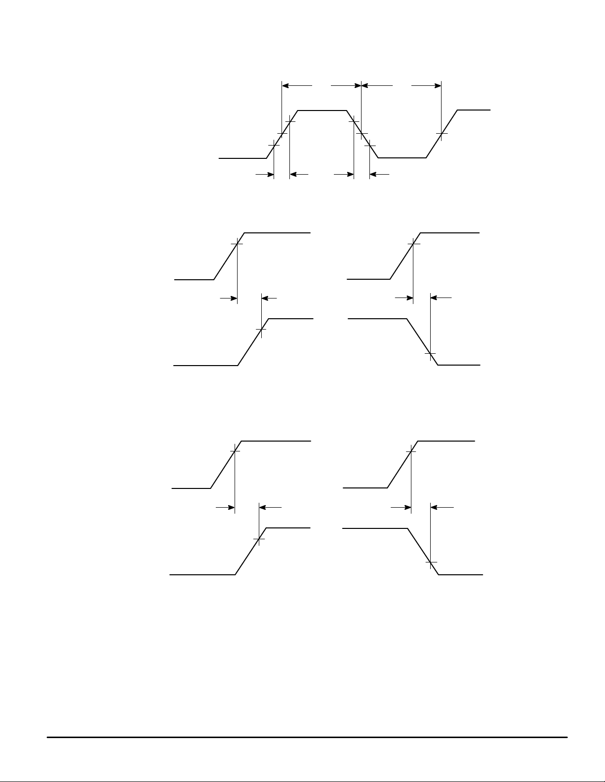
SWITCHING WAVEFORMS
CLK, TDC, RDC, RE1, CCI, MSI
MSI
VD, SO1, SO2
10%
t
w(H)
90%
50%
t
r
t
f
t
w(L)
Figure 1.
70% 70%
t
PHL
70%
t
PLH
50%
30%
TDC
Tx
Figure 2.
70% 70%
t
PLH
70%
t
PHL
Figure 3.
30%
MC145422•MC145426 MOTOROLA
6

TE1, RE1, MSI
TDC, RDC
TDC, RDC, CLK
SWITCHING WAVEFORMS (continued)
70%
t
su3
70%
Figure 4.
70%
30%
t
su5
t
h1
30%
30%
t
su4
Rx
TE1 (MC145426) OR
MSI (MC145422)
SI1, SI2
70%
30%
Figure 5.
t
su6
70%
30%
Figure 6.
30%
70%
30%
70%
t
h2
70%
30%
MC145422•MC145426MOTOROLA
7

TE1
CLK
RE1
SWITCHING WAVEFORMS (continued)
70%
t
P1
70%
Figure 7.
70%
t
P3
t
P2
70%
30%
t
P4
30%
Tx
CLK
CLK
70% 70%
Figure 8.
t
P5
70%
70%
SO1, SO2
30%
TE1
t
P6
70%
70%
30%
Figure 9.
MC145422•MC145426 MOTOROLA
8

MC145422 MASTER UDLT PIN DESCRIPTIONS
V
DD
Positive Supply
Normally 5 V.
V
SS
Negative Supply
This pin is the most negative supply pin, normally 0 V.
V
ref
Reference Output
This pin is the output of the internal reference supply and
should be bypassed to VDD and VSS by 0.1 µF capacitors.
No external dc load should be placed on this pin.
LI
Line Input
This input to the demodulator circuit has an internal
100 kΩ resistor tied to the internal reference node so that an
external capacitor and/or line transformer may be used to
couple the input signal to the part with no dc offset.
LB
Loopback Control
A low on this pin disconnects the LI pin from internal circuitry, drives LO1, LO2 to V
lator output to the demodulator input which loops the part on
itself for testing in the system. The state of this pin is internally latched if the SE pin is brought and held low. Loopback
is active only when PD
VD
Valid Data Output
A high on this pin indicates that a valid line transmission
has been demodulated. A valid transmission is determined
by proper sync and the absence of detected bit errors. VD
changes state on the leading edge of MSI when PD
When PD
tion of a line transmission. VD is a standard B–series CMOS
output and is high impedance when SE is held low.
SI1, SI2
Signaling Bit Inputs
transmission to the slave. The state of these pins is internally
latched if SE is held low.
SO1, SO2
Signaling Bit Outputs
UDLT and change state on the rising edge of MSI if PD
high, or at the completion of demodulation if PD
outputs have standard B–series CMOS drive capability and
are high impedance if the SE pin is held low.
SE
Signal Enable Input
SO1, SO2, and VD outputs function normally. If held low, the
state of these inputs is latched and held internally while the
outputs are high impedance. This allows these pins to be
bussed with those of other UDL Ts to a common controller.
is low, VD changes state at the end of demodula-
Data on these pins is loaded on the rising edge of MSI for
These outputs are received signaling bits from the slave
If held high, the PD
Is high.
, LB, SI1, SI2, and SIE inputs and the
and internally ties the modu-
ref
is high.
is low. These
is
PD
Power–Down Input
If held low, the UDLT ceases modulation. In power–down,
the only active circuit is that which is necessary to demodulate an incoming burst and output the signal and valid data
bits. Internal data transfers to the transmit and receive registers cease. When brought high, the UDLT powers up, and
waits three positive MSI edges or until the end of an incoming transmission from the slave UDLT and begins transmitting every MSI period to the slave UDLT on the next rising
edge of the MSI.
MSI
Master Sync Input
This pin is the system sync and initiates the modulation on
the twisted pair. MSI should be approximately leading–edge
aligned with TDC/RDC.
SIE
Signal Insert Enable
This pin, when held high, inserts signal bit 2 received from
the slave into the LSB of the outgoing PCM word at Tx and
will ignore the SI2 pin and use in place the LSB of the incoming PCM word at Rx for transmission to the slave. The PCM
word to the slave will have LSB forced low in this mode. In
this manner, signal bit 2 to/from the slave UDLT is inserted in
to the PCM words the master sends and receives from the
backplane for routing through the PABX for simultaneous
voice/data communication. The state of this pin is internally
latched if the SE pin is brought and held low.
TE1
Transmit Data Enable 1 Input
This pin controls the outputting of data on the Tx pin. While
TE1 is high, the Tx data is presented on the eight rising
edges of TDC/RDC. TE1 is also a high–impedance control of
the Tx pin. If MSI occurs during this period, new data will be
transferred to the Tx output register in the ninth high period of
TDC/RDC after TE1 rises; otherwise, it will transfer on the
rising edge of MSI. TE1 and TDC/RDC should be approximately leading–edge aligned.
Tx
Transmit Data Output
This three–state output presents new voice data during the
high periods of TDC/RDC when TE1 is high (see TE1).
CCI
Convert Clock Input
A 2.048 MHz clock signal should be applied to this pin. The
signal is used for internal sequencing and control. This signal
should be coherent with MSI for optimum performance but
may be asynchronous if slightly worse error rate performance can be tolerated.
TDC/RDC
Transmit/Receive Data Clock
This pin is the transmit and receive data clock and can be
64 kHz to 2.56 MHz. Data is output at the Tx pin while TE1 is
high on the eight rising edges of TDC/RDC after the rising
edge of TE1. Data on the Rx pin is loaded into the receive
register of the UDLT on the eight falling edges of TDC/RDC
after a positive transition on RE1. This clock should be approximately leading–edge aligned with MSI.
MC145422•MC145426MOTOROLA
9

Rx
Receive Data
Voice data is clocked into the UDLT from this pin on the
falling edges of TDC/RDC under the control of RE1.
RE1
Receive Data Enable 1 Input
A rising edge on this pin will enable data on the Rx pin to
be loaded into the receive data register on the next eight falling edges of the data dock, TDC/RDC. RE1 and TDC/RDC
should be approximately leading–edge aligned.
LO1, LO2
Line Driver Outputs
These outputs drive the twisted pair line with 256 kHz
modified DPSK bursts each frame and are push–pull. These
pins are driven to V
when not modulating the line.
ref
MC145426 SLAVE UDLT PIN DESCRIPTIONS
V
DD
Positive Supply
Normally 5 V.
V
SS
Negative Supply
This pin is the most negative supply pin, normally 0 V.
V
ref
Reference Output
This pin is the output of the internal reference supply and
should be bypassed to VDD and VSS by 0.1 µF capacitors.
No external dc load should be placed on this pin.
LI
Line Input
This input to the demodulator circuit has an internal
100 kΩ resistor tied to the internal reference node (V
that an external capacitor and/or line transformer may be
used to couple the signal to this part with no dc offset.
LB
Loopback Control
When this pin is held low and PD
ceiving transmissions from the master), the UDLT will use
the 8 bits of demodulated PCM data in place of the 8 bits of
Rx data in the return burst to the Master, thereby looping the
part back on itself for system testing. SI1 and SI2 operate
normally in this mode. CLK will be held low during loopback
operation.
VD
Valid Data Output
A high on this pin indicates that a valid line transmission has
been demodulated. A valid transmission is determined by
proper sync and the absence of detected bit errors.VD
changes state on the leading edge of TE1. If no transmissions
from the master have been received in the last 250 µs
(derived from the internal oscillator), VD will go low without
TE1 rising since TE1 is not generated in the absence of received transmissions from the master (see TE pin description for the one exception to this).
is high (the UDLT is re-
ref
) so
SI1, SI2
Signaling Bit Inputs
Data on these pins is loaded on the rising edge of TE1 for
transmission to the master. If no transmissions from the
master are being received and PD
will be loaded into the part on an internal signal. Therefore,
data on these pins should be steady until synchronous
communication with the master has been established, as indicated by the high on VD.
SO1, SO2
Signaling Bit Outputs
These outputs are received signaling bits from the master
UDLT and change state on the rising edge of TE1. These
outputs have standard B–series CMOS output drive capability.
PD
Power–Down Input/Output
This is a bidirectional pin with weak output drivers such
that it can be overdriven externally . When held low , the UDLT
is powered down and the only active circuitry is that which is
necessary for demodulation, TE1/RE1/CLK generation upon
demodulation, the outputting of data received from the master, and updating of VD status. When held high, the UDLT is
powered up and transmits in response to transmissions from
the master. If no received bursts from the master have occurred when powered up for 250 µs (derived from the internal
oscillator frequency), the UDLT will generate a free running
125 µs internal clock from the internal oscillator and will burst
a transmission to the master every other internal 125 µs
clock using data on the SI1 and SI2 pins and the last data
word loaded into the receive register. The weak output drivers will try to force PD
master is demodulated and will try to force it low if 250 µs
have passed without a transmission from the master. This allows the slave UDLT to self power–up and down in demand
powered loop systems.
TE
T one Enable
A high on this pin generates a 500 Hz square wave PCM
tone and inserts it in place of the demodulated voice PCM
word from the master for outputting to the Tx pin to the telset
mono–circuit. A high on TE will generate TE1 and CLK from
the internal oscillator when the slave is not receiving bursts
from the master so that the PCM square wave can be loaded
into the codec–filter. This feature allows the user to provide
audio feedback for the telset keyboard depressions except
during loopback. During loopback of the slave UDLT, CLK is
defeated so a tone cannot be generated in this mode.
TE1
Transmit Data Enable 1 Output
This is a standard B–series CMOS output which goes
high after the completion of demodulation of an incoming
transmission from the master. It remains high for 8 CLK
periods and then low until the next burst from the master is
demodulated. While high, the voice data just demodulated is
output on the first eight rising edges of CLK at the Tx pin. The
signaling data just demodulated is output on SO1 and SO2
on TE1’s rising edge, as is VD.
high when a transmission from the
is high, data on these pins
MC145422•MC145426 MOTOROLA
10

Tx
Transmit Data Output
This is a standard B–series CMOS output. Voice data is
output on this pin on the rising edges of CLK while TE1 is
high and is high impedance when TE1 is low.
X1
Crystal Input
A 4.096 MHz crystal is tied between this pin and X2. A
10 MΩ resistor across X1 and X2 and 25 pF capacitors from
X1 and X2 to VSS are required for stability and to ensure
startup. X1 may be driven by an external CMOS clock signal
if X2 is left open.
X2
Crystal Output
This pin is capable of driving one external CMOS input and
15 pF of additional capacitance (see X1 pin description).
CLK
Clock Output
This is a standard B–series CMOS output which provides
the data clock for the telset codec–filter. It is generated by dividing the oscillator down to 128 kHz and starts upon the
completion of demodulation of an incoming burst from the
master. At this time, CLK begins and TE1 goes high. CLK will
remain active for 16 periods, at the end of which it will remain
low until another transmission from the master is demodulated. In this manner, sync from the master is established in
the slave and any clock slip between the master and the
slave is absorbed each frame. CLK is generated in response
to an incoming burst from the master, however, if TE is
brought high, then CLK and TE1/RE1 are generated from the
internal oscillator until TE is brought low or an incoming burst
from the master is received. CLK is disabled when LB
low.
Rx
Receive Data Input
Voice data from the telset codec–filter is input on this pin
on the first eight falling edges of CLK after RE1 goes high.
Mu/A
T one Digital Format Input
This pin determines if the PCM code of the 500 Hz square
wave tone, when TE is high, is Mu–Law (Mu/A = 1) or A–Law
(Mu/A = 0) format.
RE1
Receive Data Enable 1 Output
This is a standard B–series CMOS output which is the
inverse of TE1 (see TE1 pin description).
LO1, LO2
Line Driver Outputs
These outputs drive the twisted pair line with 256 kHz
modified DPSK bursts each frame and are push–pull. These
pins are driven to V
when the device is not modulating.
ref
is held
BACKGROUND
The MC145422 master and MC145426 slave UDLT transceiver ICs main application is to bidirectionally transmit the
digital signals present at a codec–filter digital–PABX backplane interface over normal telephone wire pairs. This allows
the remoting of the codec–filter in a digital telephone set and
enables each set to have a high speed data access to the
PABX switching facility. In effect, the UDLT allows each
PABX subscriber direct access to the inherent 64 kbps data
routing capabilities of the PABX.
The UDLT provides a means for transmitting and receiving
64 kbits of voice data and 16 kbps of signaling data in two–
wire format over normal telephone pairs. The UDL T is a two–
chip set consisting of a master and a slave. The master
UDLT replaces the codec–filter and SLIC on the PABX line
card, and transmits and receives data over the wire pair to
the teleset. The UDL T appears to the linecard and backplane
as if it were a PCM Codec–Filter and has almost the same
digital interface features as the MC145500 series codec–filters. The slave UDLT is located in the telset and interfaces
the codec–filter to the wire pair. By hooking two UDLTs back–
to–back, a repeater can also be formed. The master and
slave UDLTs operate in a frame synchronous manner, sync
being established at the slave by the timing of the master’s
transmission. The master’s sync is derived from the PABX
frame sync.
The UDLT operates using one twisted pair. Eight bits of
voice data and two bits of signaling data are transmitted and
received each frame in a half–duplex manner (i.e., the slave
waits until the transmission from the master is completely received before transmitting back to the master). Transmission
occurs at 256 kHz bit rate using a modified form of DPSK.
This “ping– pong” mode will allow transmission of data at distances up to two kilometers before turnaround delay becomes a problem. The UDLT is so defined as to allow this
data to be handled by the linecard, backplane, and PABX as
if it were just another voice conversation. This allows existing
PABX hardware and software to be unchanged and yet provides switc hed 64 kbps voice or data communications
throughout its service area by simply replacing a subscriber’s linecard and teleset. A feature in the master allows one
of the two signaling bits to be inserted and extracted from the
backplane PCM word to allow simultaneous voice and data
transmission through the PABX. Both UDLTs have a loopback feature by which the device can be tested in the user
system.
The slave UDLT has the additional feature of providing a
500 Hz Mu–Law or A–Law coded square wave to the codec–
filter when the TE pin is brought high. This can be used to
provide audio feedback in the telset during keyboard depressions.
CIRCUIT DESCRIPTION
GENERAL
The UDL T consists of a modulator, demodulator, two intermediate data buffers, sequencing and control logic, and
transmit and receive data registers. The data registers
interface to the linecard or codec–filter digital interface signals, the modulator and demodulator interface the twisted
pair transmission medium, while the intermediate data registers buffer data between these two sections. The UDLT is
MC145422•MC145426MOTOROLA
11

intended to operate on a single 5 V supply and can be driven
by TTL or CMOS logic.
MASTER OPERATION
In the master, data from the linecard is loaded into the receive register each frame from the Rx pin under the control of
the TDC/RDC clock and the receive data enable, RE1. RE1
controls loading of eight serial bits, henceforth referred to as
the voice data word. Each MSI, these words are transferred
out of the receive register to the modulation buffer for subsequent modulation onto the line. The modulation buffer takes
the receive voice data word and the two signaling data input
bits on SI1 and SI2 loaded on the MSI transition and formats
the 10 bits into a specific order. This data field is then transmitted in a 256 kHz modified DPSK burst onto the line to the
remote slave UDLT.
Upon demodulating the return burst from the slave, the decoded data is transferred to the demodulation buffer and the
signaling bits are stripped ready to be output on SO1 and
SO2 at the next MSI. The voice data word is loaded into the
transmit register as described in the TE1 pin description for
outputting via the Tx pin at the TDC/RDC data clock rate under the control of TE1. VD is output on the rising edge of MSI.
Timing diagrams for the master are shown in Figure 10.
SLAVE OPERATION
In the slave, the synchronizing event is the detection of an
incoming line transmission from the master as indicated by
the completion of demodulation. When an incoming burst
from the master is demodulated, several events occur. As in
the master, data is transferred from the demodulator to the
demodulation buffer and the signaling bits are stripped for
outputting at SO1 and SO2. Data in the receive register is
transferred to the modulation buffer . TE1 goes high loading in
data at SI1 and SI2, which will be used in the transmission
burst to the master along with the data in the transmit data
buffer, and outputting SO1, SO2, and VD. Modulation of the
burst begins four 256 kHz periods after the completion of demodulation.
While TE1 is high, voice data is output on Tx to the telset
codec–filter on the rising edges of the data clock output on
the CLK pin. On the ninth rising edge of CLK, TE1 goes low,
RE1 goes high, and voice data from the codec–filter is input
to the receiver register from the Rx pin on the next eight
falling edges of CLK. RE1 is TE1 inverted and is provided to
facilitate interface to the codec–filter.
The CLK pin 128 kHz output is formed by dividing down
the 4.096 MHz crystal frequency by 32. Slippage between
the frame rate of the master (as represented by the completion of demodulation of an incoming transmission from the
master) and the crystal frequency is absorbed by holding the
16th low period of CLK until the next completion of demodulation. This is shown in the slave UDL T timing diagram of Figure 11.
POWER–DOWN OPERATION
In the master when PD
and only that circuitry necessary to demodulate the incoming
bursts and output the signaling and VD data bits is active. In
this mode, if the UDLT receives a burst from the slave, the
SO1, SO2, and VD pins will change state upon completion of
the demodulation instead of the the rising edge of MSI. The
state of these pins will not change until either three rising MSI
edges have occurred without the reception of a burst from
the slave or until another burst is demodulated, whichever
occurs first.
When PD
three rising MSI edges or until the MSI rising edge following
the demodulation of an incoming burst before transmitting to
the slave. The data for the first transmission to the slave after
power–up is loaded into the UDLT during the RE1 period
prior to the burst in the case of voice, and on the present rising edge of MSI for signaling data.
In the slave, PD
drivers such that it can be overdriven externally. When held
low, the UDLT slave is powered–down and only that circuitry
necessary for demodulation, TE1/RE1/CLK generation upon
demodulation, and the outputting of voice and signaling bits
is active. When held high, the UDLT slave is powered–up
and transmits normally in response to transmissions from the
master. If no bursts have been received from the master
within 250 µs after power–up (derived from the internal oscillator frequency), the UDLT generates an internal 125 µs
free–running clock from the internal oscillator. The slave
UDLT then bursts a transmission to the master UDLT every
other 125 µs clock period using data loaded into the Rx pin
during the last RE1 period and SI1, SI2 data loaded in on the
internal 125 µs clock edge. The weak output drivers will try to
force PD
dulated and will try to force it low if 250 µs have passed without a transmission from the master. This allows the slave
UDLT to self power–up and down in demand power–loop
systems.
is brought high, the master UDL T will wait either
high when a transmission from the master is demo-
is low, the UDLT stops modulating
is a bidirectional pin with weak output
MC145422•MC145426 MOTOROLA
12

125 µs
MSI
CCI/TDC/RDC
TE1
Tx
RE1
Rx
SI1, SI2
SO1, SO2
VD
DEMODULA TOR
SYNC
OUT (INTERNAL)
THREE–STATE
VALID DATA
VALID
••••••••••••••••••••••••••••••••••••••••••••••••••••••
••••••••••••••••••••••••••••••••••••••••••••••••••••••
TRANSFER RECEIVE REGISTER TO MODULA TION BUFFER, LATCH VALID DATA PIN,
LATCH SI1, SI2. TWO CCI CLOCKS LATER, TRANSFER RECEIVE REGISTER TO
MODULA TION BUFFER, START MODULATION.
DON’T CARE
•••
DON’T CARE
VALID
TRANSFER DEMODULAT OR
DATA TO DEMODULATION
BUFFER
••
IN
IN
IN
OUT
IN
IN
IN
OUT
OUT
Figure 10. Master UDL T Timing
MC145422•MC145426MOTOROLA
13

DEMODULATOR
SYNC (INTERNAL)
CLK (128 kHz)
INTERNAL
2.048 MHz FROM XTAL
TE1
RE1
Tx
µ
s
125
•
•
•
•
•
•
•
•
•
•
•
•
•
NOTE 1
•
•
•
•
•
•
•
•
•
•
•
•
•
••• ••• ••••
•
•
•
•
•
•
VOICE
HIGH IMPEDANCE
•
•
•
•
•
•
Rx
SI1, SI2
SO1, SO2
VD
DON’T CARE
DON’T CARE
TRANSFER DEMODULA TION BUFFER TO TRANSMIT REGISTER, GENERATE ENABLES,
LATCH SI1, SI2, OUTPUT Tx, SO1, SO2, OUTPUT VALID DAT A, START 128 kHz CLOCK, START
MODULA TION AFTER FOUR 256 kHz BAUD PERIODS.
DEMODULATION DATA TRANSFER TO
DEMODULA TION BUFFER
NOTE: 1. Slip between master and slave is taken up in this period.
Figure 11. Slave UDLT Timing
VOICE
MC145422•MC145426 MOTOROLA
14

Both the Differential–Phase Shift Keying and the Modified
Differential–Phase–Shift Keying waveforms are shown in
Figures 12 thru 14. The DPSK encodes data as phase reversals of a 256 kHz carrier. A 0 is indicated by a 180° phase
shift between bit boundaries, while the signal continues in
phase to indicate a 1. This method needs no additional bits
to indicate the start of the burst.
The modified DPSK waveform actually used in the transceivers is a slightly modified form of DPSK, as shown in Figure 12. The phase–reversal cusps of the DPSK waveform
have been replaced by a 128 kHz half–cycle to lower the
DIFFERENTIAL–PHASE–SHIFT KEYING
MODIFIED DIFFERENTIAL–PHASE–SHIFT KEYING
spectral content of the waveform, which, save for some key
differences, appears quite similar to frequency shift keying.
The burst always begins and ends with a half–cycle of
256 kHz, which helps locate bit boundaries.
The bit pattern shown in Figure 13a shows a stable waveform due to the even number of phase changes or zeros. The
waveform shown in Figure 13b shows random data patterns
being modulated.
Figure 14 shows the “ping–pong” signals on 3000 feet of
26 AWG twisted–pair wire as viewed at LI of the master
UDLT and the slave UDLT.
1111
00000
1
Figure 12. Modified Differential Phase Shift Keying
13a. Bit Pattern — 1010101000 13b. Bit Pattern — Random
Figure 13. T ypical Signal Waveforms at Demodulator
MC145422•MC145426MOTOROLA
15

MASTER
SLAVE
BIT PATTERN — 1010101000
BIT PATTERN — RANDOM
Figure 14. T ypical Signal Waveforms at Demodulator
MC145422•MC145426 MOTOROLA
16

TO
BACKPLANE
8 kHz FRAME SYNC
TRANSMIT DATA BUS
RECEIVE DATA BUS
2.048 MHz DATA CLOCK
TO
BACKPLANE
TIMING
AND
CONTROL
POWER
SUPPLY
121518171611191413101
Tx
Rx
CCIPDRE1
T/RDC
ref
LO1VLO2LISI1
3687954
110 110
N = 2N = 0.5
SI2
110
110
MSI
DD
V
22
21220
SIE
TE1
SO1
SO2VDLB
F
µ
0.1
SE
V
SS
F
µ
0.1
MC145422
5.1 k
5.1 k
N = 4
N = 0.5
POWER
SUPPLY
121518171611191413101
Tx
Rx
MSI
DD
ref
V
LO1VLO2LISI1
22
21220
110
CCIPDRE1
T/RDC
3687954
N = 2N = 0.5
SI2
110
TE1
SO1
110
SE
SIE
SO2VDLB
V
SS
F
µ
0.1
MC145422
F
µ
5.1 k
0.1
5.1 k
N = 4
N = 0.5
TIP
RING
TIP 110
Figure 15. T ypical Multichannel Digital Line Card
RING
MC145422•MC145426MOTOROLA
17

TIP
RING
N = 0.5
T1
ΩΩ
4.7 k
5 V
4.7 k
5 V
22114
DD
V
Tx
1413181917812
PD
TE1
LB
Rx
N = 4
3
LI
RE1
2
ref
V
CLK
5
212010
VD
LO1
UDLT
MC145426
SI2
TE
Ω
110
Ω
110
7
LO2
SO1
9
N = 0.5
N = 2
8
Mu/A
SO2
15
Ω
110
Ω
110
1
SI1
V
X2
X1
18
Ω
10 M
SS
20 pF20 pF
4.096 MHz
Ω
20
F
µ
50
Ω
10 k
10 V
2 W
33 V
5 V
LM317 78M05
Ω
270
10 V
F
µ
4.7
F
µ
4.7
SPEAKER
Ω
1.8 k
F
µ
0.1
+5 V
10 V
1514111012
RDD
DD
V
6
16
10 V
Ω
10 k
F
µ
0.1
TDD
RCE
Mu/A
PD
7
XMTR
1398
TDE
TDC
RDC
MONO-
CIRCUIT
MC145503
RxO
Tx–
TxI
5
4
2
Ω
1.6 k
56 k
ΩΩ
3.6 k
3
LS
V
Tx+
SS
V
AG
V
1
RCVR
5 V
Ω
100 k
AG
V
S1B OPEN = ON HOOK
AG
S1A CLOSED = ON HOOK
V
Figure 16. Basic Digital T elset
181712
DTMF OUT
Ω
100 k
DD
V
1
OPL
COL1
3
7
OH/T
COL2
4
11
TSO
PULSE/TONE
COL3
5
Ω
47 k
10
MS
MO
DIALER
COL4
ROW1
2
161514
8
in
OSC
ROW2
ROW3
MHz
3.579545
9
out
OSC
SS
V
ROW4
6
13
= ANALOG GROUND
= DIGITAL GROUND
MC145422•MC145426 MOTOROLA
18

10 V
Ω
10 k
SPEAKER
+5 V
R2
Ω
10 k
S3
HOOK
SWITCH
T1
TIP
RING
N = 1
11
10 98
PD
Mu/A
TE
TE1TxX1
12
13
S2 – SW1
C1
20 pF
SI2
SO2
141516
Y1
Ω
R1
10 M
20 pF
Ω
R3
5 k
7
6
5
SI1
SO1
MC145426
X2
4.096 MHz
C2
+ 5 V
NC
4
LB
VD
CLKRxRE1
171819
Ω
R11
5 k
D1
5 k
3
LI
LO2
LO1
202122
D2
N = 4
2
ref
V
DD
V
F
µ
0.1
C8
F
µ
C9
0.1
1
SS
V
+5 V
R10
D3
Ω
110
Ω
110
D4
N = 2
R9
D5
Ω
110
D6
Ω
110
+5 V
– 5 V
F
µ
C13
10
2221201918171615141312
DD
RSI
ref
V
1
2
V
V
AG
RDD
RxO
3
R5
RCE
RxG
4
Ω
5 k
V
AG
CCI
TDC
RDC
MC145502
RxO
+Tx
5
6
R7
Ω
R6
500
F
µ
0.1
Ω
10 k
R8
R13
Figure 17. Full–Featured Digital T elset
TDD
TxI
7
TDE
–Tx
8
Ω
56 k
Ω
10 k
C4
MSI
Mu/A
9
Ω
1 k
LS
V
PDI
10
F
µ
10
R12
SS
V
11
– 5 V
C12
= ANALOG GROUND
+5 V
= DIGITAL GROUND
MC145422•MC145426MOTOROLA
19

P ACKAGE DIMENSIONS
P SUFFIX
PLASTIC PACKAGE
CASE 708–04
1222
B
111
A
N
C
K
DFGH
–T–
SEATING
PLANE
SEATING
PLANE
SOG PACKAGE
CASE 751E–04
–A–
1324
–B–
12X
1
12
D24X
0.010 (0.25) B
M
S
A
T
S
C
G22X
K
M
DW SUFFIX
P
0.010 (0.25) B
J
F
NOTES:
1. POSITIONAL TOLERANCE OF LEADS (D),
SHALL BE WITHIN 0.25 (0.010) AT MAXIMUM
MATERIAL CONDITION, IN RELATION TO
SEATING PLANE AND EACH OTHER.
2. DIMENSION L TO CENTER OF LEADS WHEN
FORMED PARALLEL.
3. DIMENSION B DOES NOT INCLUDE MOLD
FLASH.
MILLIMETERS INCHES
MIN MINMAX MAX
L
J
M
M
R
X 45
M
DIM
27.56
A
8.64
B
3.94
C
0.36
D
1.27
F
2.54 BSC
G
1.02
H
0.20
J
2.92
K
10.16 BSC
L
M
°
0
0.51
N
NOTES:
1. DIMENSIONING AND TOLERANCING PER ANSI
Y14.5M, 1982.
2. CONTROLLING DIMENSION: MILLIMETER.
3. DIMENSIONS A AND B DO NOT INCLUDE
MOLD PROTRUSION.
4. MAXIMUM MOLD PROTRUSION 0.15 (0.006)
PER SIDE.
5. DIMENSION D DOES NOT INCLUDE DAMBAR
PROTRUSION. ALLOWABLE DAMBAR
PROTRUSION SHALL BE 0.13 (0.005) TOTAL IN
EXCESS OF D DIMENSION AT MAXIMUM
MATERIAL CONDITION.
DIM MIN MAX MIN MAX
A 15.25 15.54 0.601 0.612
B 7.40 7.60 0.292 0.299
C 2.35 2.65 0.093 0.104
D 0.35 0.49 0.014 0.019
_
F 0.41 0.90 0.016 0.035
G 1.27 BSC 0.050 BSC
J 0.23 0.32 0.009 0.013
K 0.13 0.29 0.005 0.011
M 0 8 0 8
P 10.05 10.55 0.395 0.415
R 0.25 0.75 0.010 0.029
28.32
9.14
5.08
0.56
1.78
1.52
0.38
3.43
15
1.02
°
1.085
0.340
0.155
0.014
0.050
0.100 BSC
0.040
0.008
0.115
0.400 BSC
°
0
0.020
INCHESMILLIMETERS
1.115
0.360
0.200
0.022
0.070
0.060
0.015
0.135
15
0.040
°
____
Motorola reserves the right to make changes without further notice to any products herein. Motorola makes no warranty, representation or guarantee regarding
the suitability of its products for any particular purpose, nor does Motorola assume any liability arising out of the application or use of any product or circuit,
and specifically disclaims any and all liability, including without limitation consequential or incidental damages. “T ypical” parameters can and do vary in different
applications. All operating parameters, including “T ypicals” must be validated for each customer application by customer’s technical experts. Motorola does
not convey any license under its patent rights nor the rights of others. Motorola products are not designed, intended, or authorized for use as components in
systems intended for surgical implant into the body, or other applications intended to support or sustain life, or for any other application in which the failure of
the Motorola product could create a situation where personal injury or death may occur. Should Buyer purchase or use Motorola products for any such
unintended or unauthorized application, Buyer shall indemnify and hold Motorola and its officers, employees, subsidiaries, affiliates, and distributors harmless
against all claims, costs, damages, and expenses, and reasonable attorney fees arising out of, directly or indirectly, any claim of personal injury or death
associated with such unintended or unauthorized use, even if such claim alleges that Motorola was negligent regarding the design or manufacture of the part.
Motorola and are registered trademarks of Motorola, Inc. Motorola, Inc. is an Equal Opportunity/Af firmative Action Employer.
How to reach us:
USA/EUROPE: Motorola Literature Distribution; JAPAN: Nippon Motorola Ltd.; Tatsumi–SPD–JLDC, Toshikatsu Otsuki,
P.O. Box 20912; Phoenix, Arizona 85036. 1–800–441–2447 6F Seibu–Butsuryu–Center, 3–14–2 Tatsumi Koto–Ku, Tokyo 135, Japan. 03–3521–8315
MFAX: RMF AX0@email.sps.mot.com – T OUCHTONE (602) 244–6609 HONG KONG: Motorola Semiconductors H.K. Ltd.; 8B T ai Ping Industrial Park,
INTERNET: http://Design–NET.com 51 Ting Kok Road, Tai Po, N.T., Hong Kong. 852–26629298
MC145422•MC145426 MOTOROLA
20
◊
*MC145422/D*
MC145422/D
 Loading...