

Datasheet MC14538BCP, MC14538BD, MC14538BDR2, MC14538BDT, MC14538BDTR2 Datasheet (MOTOROLA)
...
Semiconductor Components Industries, LLC, 2000
March, 2000 – Rev. 3
1 Publication Order Number:
MC14538B/D
MC14538B
Dual Precision
Retriggerable/Resettable
Monostable Multivibrator
The MC14538B is a dual, retriggerable, resettable monostable
multivibrator. It may be triggered from either edge of an input pulse,
and produces an accurate output pulse over a wide range of widths, the
duration and accuracy of which are determined by the external timing
components, C
X
and RX.
Output Pulse Width = (Cx) (Rx) where:
Rx is in k
W
Cx is in mF
• Unlimited Rise and Fall Time Allowed on the A Trigger Input
• Pulse Width Range = 10 µs to 10 s
• Latched Trigger Inputs
• Separate Latched Reset Inputs
• 3.0 Vdc to 18 Vdc Operational Limits
• Triggerable from Positive (A Input) or Negative–Going Edge
(B–Input)
• Capable of Driving Two Low–power TTL Loads or One Low–power
Schottky TTL Load Over the Rated Temperature Range
• Pin–for–pin Compatible with MC14528B and CD4528B (CD4098)
• Use the MC54/74HC4538A for Pulse Widths Less Than 10 µs with
Supplies Up to 6 V.
MAXIMUM RATINGS (Voltages Referenced to V
SS
) (Note 2.)
Symbol Parameter Value Unit
V
DD
DC Supply Voltage Range –0.5 to +18.0 V
Vin, V
out
Input or Output Voltage Range
(DC or Transient)
–0.5 to VDD + 0.5 V
Iin, I
out
Input or Output Current
(DC or Transient) per Pin
±10 mA
P
D
Power Dissipation,
per Package (Note 3.)
500 mW
T
A
Operating Temperature Range –55 to +125 °C
T
stg
Storage Temperature Range –65 to +150 °C
T
L
Lead Temperature
(8–Second Soldering)
260 °C
2. Maximum Ratings are those values beyond which damage to the device
may occur.
3. Temperature Derating:
Plastic “P and D/DW” Packages: – 7.0 mW/_C From 65_C T o 125_C
This device contains protection circuitry to guard against damage due to high
static voltages or electric fields. However, precautions must be taken to avoid
applications of any voltage higher than maximum rated voltages to this
high–impedance circuit. For proper operation, V
in
and V
out
should be constrained
to the range V
SS
v (Vin or V
out
) v VDD.
Unused inputs must always be tied to an appropriate logic voltage level (e.g.,
either V
SS
or VDD). Unused outputs must be left open.
http://onsemi.com
A = Assembly Location
WL or L = Wafer Lot
YY or Y = Year
WW or W = Work Week
Device Package Shipping
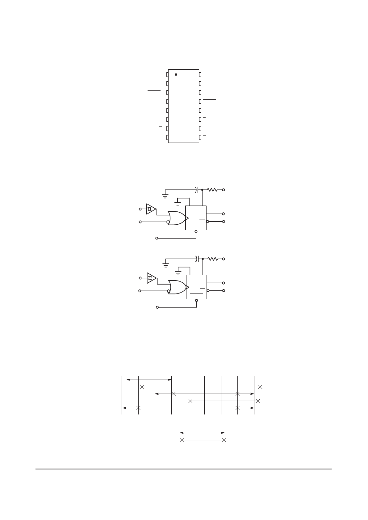
ORDERING INFORMATION
MC14538BCP PDIP–16 2000/Box
MC14538BD SOIC–16 48/Rail
MARKING
DIAGRAMS
1
16
PDIP–16
P SUFFIX
CASE 648
MC14538BCP
AWLYYWW
MC14538BDR2 SOIC–16 2500/Tape & Reel
SOIC–16
DW SUFFIX
CASE 751G
1
16
14538B
AWLYYWW
1. For ordering information on the EIAJ version of
the SOIC packages, please contact your local
ON Semiconductor representative.
SOEIAJ–16
F SUFFIX
CASE 966
1
16
MC14538B
AWLYWW
MC14538BDT TSSOP–16 96/Rail
SOIC–16
D SUFFIX
CASE 751B
1
16
14538B
AWLYWW
TSSOP–16
DT SUFFIX
CASE 948F
14
538B
ALYW
1
16
MC14538BDTR2 TSSOP–16 2500/Tape & Reel
MC14538BDW SOIC–16 47/Rail
MC14538BDWR2 SOIC–16 1000/Tape & Reel
MC14538BF SOEIAJ–16 See Note 1.
MC14538BFEL SOEIAJ–16 See Note 1.
MC14538B
http://onsemi.com
2
PIN ASSIGNMENT
13
14
15
16
9
10
11
125
4
3
2
1
8
7
6
A
B
RESET B
C
X/RX
B
V
SS
V
DD
Q
B
Q
B
B
B
A
A
RESET A
C
X/RX
A
V
SS
V
SS
Q
A
Q
A
B
A
BLOCK DIAGRAM
V
DD
V
DD
6
7
10
9
12
11
5
4
A
B
C
X
R
X
12
Q1
Q1
RESET
3
C
X
R
X
15 14
Q2
Q2
RESET
13
A
B
RX AND CX ARE EXTERNAL COMPONENTS.
V
DD
= PIN 16
V
SS
= PIN 8, PIN 1, PIN 15
ONE–SHOT SELECTION GUIDE
100 ns
MC14528B
MC14536B
MC14538B
MC14541B
MC4538A*
1 µs 10 µs 100 µs 1 ms 10 ms 100 ms 1 s 10 s
*LIMITED OPERATING VOLTAGE (2 – 6 V)
TOTAL OUTPUT PULSE WIDTH RANGE
RECOMMENDED PULSE WIDTH RANGE
23 HR
5 MIN.
MC14538B
http://onsemi.com
3
ELECTRICAL CHARACTERISTICS (Voltages Referenced to V
SS
)
V
DD
– 55_C 25_C 125_C
Characteristic Symbol
Vdc
Min Max Min Typ
(4.)
Max Min Max
Unit
Output Voltage “0” Level
V
in
= VDD or 0
V
OL
5.0
10
15
—
—
—
0.05
0.05
0.05
—
—
—
0
0
0
0.05
0.05
0.05
—
—
—
0.05
0.05
0.05
Vdc
“1” Level
V
in
= 0 or V
DD
V
OH
5.0
10
15
4.95
9.95
14.95
—
—
—
4.95
9.95
14.95
5.0
10
15
—
—
—
4.95
9.95
14.95
—
—
—
Vdc
Input Voltage “0” Level
(V
O
= 4.5 or 0.5 Vdc)
(V
O
= 9.0 or 1.0 Vdc)
(V
O
= 13.5 or 1.5 Vdc)
V
IL
5.0
10
15
—
—
—
1.5
3.0
4.0
—
—
—
2.25
4.50
6.75
1.5
3.0
4.0
—
—
—
1.5
3.0
4.0
Vdc
“1” Level
(V
O
= 0.5 or 4.5 Vdc)
(V
O
= 1.0 or 9.0 Vdc)
(V
O
= 1.5 or 13.5 Vdc)
V
IH
5.0
10
15
3.5
7.0
11
—
—
—
3.5
7.0
11
2.75
5.50
8.25
—
—
—
3.5
7.0
11
—
—
—
Vdc
Output Drive Current
(V
OH
= 2.5 Vdc) Source
(V
OH
= 4.6 Vdc)
(V
OH
= 9.5 Vdc)
(V
OH
= 13.5 Vdc)
I
OH
5.0
5.0
10
15
– 3.0
– 0.64
– 1.6
– 4.2
—
—
—
—
– 2.4
– 0.51
– 1.3
– 3.4
– 4.2
– 0.88
– 2.25
– 8.8
—
—
—
—
– 1.7
– 0.36
– 0.9
– 2.4
—
—
—
—
mAdc
(VOL = 0.4 Vdc) Sink
(V
OL
= 0.5 Vdc)
(V
OL
= 1.5 Vdc)
I
OL
5.0
10
15
0.64
1.6
4.2
—
—
—
0.51
1.3
3.4
0.88
2.25
8.8
—
—
—
0.36
0.9
2.4
—
—
—
mAdc
Input Current, Pin 2 or 14 I
in
15 — ±0.05 — ±0.00001 ±0.05 — ±0.5 µAdc
Input Current, Other Inputs I
in
15 — ±0.1 — ±0.00001 ±0.1 — ±1.0 µAdc
Input Capacitance, Pin 2 or 14 C
in
— — — — 25 — — — pF
Input Capacitance, Other Inputs
(V
in
= 0)
C
in
— — — — 5.0 7.5 — — pF
Quiescent Current
(Per Package)
Q = Low, Q
= High
I
DD
5.0
10
15
—
—
—
5.0
10
20
—
—
—
0.005
0.010
0.015
5.0
10
20
—
—
—
150
300
600
µAdc
Quiescent Current, Active State
(Both) (Per Package)
Q = High, Q
= Low
I
DD
5.0
10
15
—
—
—
2.0
2.0
2.0
—
—
—
0.04
0.08
0.13
0.20
0.45
0.70
—
—
—
2.0
2.0
2.0
mAdc
Total Supply Current at an external
load capacitance (C
L
) and at
external timing network (R
X
, CX)
(5.)
I
T
5.0
10
IT = (3.5 x 10⁻²) RXCXf + 4CXf + 1 x 10⁻⁵ CLf
I
T
= (8.0 x 10⁻²) RXCXf + 9CXf + 2 x 10⁻⁵ CLf
I
T
= (1.25 x 10⁻¹) RXCXf + 12CXf + 3 x 10⁻⁵ CLf
where: I
T
in µA (one monostable switching only),
where: C
X
in µF, CL in pF, RX in k ohms, and
where: f in Hz is the input frequency.
µAdc
4. Data labelled “Typ” is not to be used for design purposes but is intended as an indication of the IC’s potential performance.
5. The formulas given are for the typical characteristics only at 25_C.
MC14538B
http://onsemi.com
4
SWITCHING CHARACTERISTICS
(6.)
(C
L
= 50 pF, T
A
= 25_C)
V
All Types
Characteristic Symbol
V
DD
Vdc
Min Typ
(7.)
Max
Unit
Output Rise Time
t
TLH
= (1.35 ns/pF) CL + 33 ns
t
TLH
= (0.60 ns/pF) CL + 20 ns
t
TLH
= (0.40 ns/pF) CL + 20 ns
t
TLH
5.0
10
15
—
—
—
100
50
40
200
100
80
ns
Output Fall Time
t
THL
= (1.35 ns/pF) CL + 33 ns
t
THL
= (0.60 ns/pF) CL + 20 ns
t
THL
= (0.40 ns/pF) CL + 20 ns
t
THL
5.0
10
15
—
—
—
100
50
40
200
100
80
ns
Propagation Delay Time
A or B to Q or Q
t
PLH
, t
PHL
= (0.90 ns/pF) CL + 255 ns
t
PLH
, t
PHL
= (0.36 ns/pF) CL + 132 ns
t
PLH
, t
PHL
= (0.26 ns/pF) CL + 87 ns
t
PLH
,
t
PHL
5.0
10
15
—
—
—
300
150
100
600
300
220
ns
Reset to Q or Q
t
PLH
, t
PHL
= (0.90 ns/pF) CL + 205 ns
t
PLH
, t
PHL
= (0.36 ns/pF) CL + 107 ns
t
PLH
, t
PHL
= (0.26 ns/pF) CL + 82 ns
5.0
10
15
—
—
—
250
125
95
500
250
190
ns
Input Rise and Fall Times
Reset
tr, t
f
5
10
15
—
—
—
—
—
—
15
5
4
µs
B Input 5
10
15
—
—
—
300
1.2
0.4
1.0
0.1
0.05
ms
A Input 5
10
15
No Limit
—
Input Pulse Width
A, B, or Reset
tWH,
t
WL
5.0
10
15
170
90
80
85
45
40
—
—
—
ns
Retrigger Time t
rr
5.0
10
15
0
0
0
—
—
—
—
—
—
ns
Output Pulse Width — Q or Q
Refer to Figures 8 and 9
C
X
= 0.002 µF, RX = 100 kΩ
T
5.0
10
15
198
200
202
210
212
214
230
232
234
µs
CX = 0.1 µF, RX = 100 kΩ 5.0
10
15
9.3
9.4
9.5
9.86
10
10.14
10.5
10.6
10.7
ms
CX = 10 µF, RX = 100 kΩ 5.0
10
15
0.91
0.92
0.93
0.965
0.98
0.99
1.03
1.04
1.06
s
Pulse Width Match between circuits in
the same package.
C
X
= 0.1 µF, RX = 100 kΩ
100
[(T
1
– T2)/T1]
5.0
10
15
—
—
—
± 1.0
± 1.0
± 1.0
± 5.0
± 5.0
± 5.0
%
6. The formulas given are for the typical characteristics only at 25_C.
7. Data labelled “Typ” is not to be used for design purposes but is intended as an indication of the IC’s potential performance.

MC14538B
http://onsemi.com
5
OPERATING CONDITIONS
External Timing Resistance R
X
— 5.0 —
(8.)
kΩ
External Timing Capacitance C
X
— 0 — No
Limit
(9.)
µF
8. The maximum usable resistance RX is a function of the leakage of the capacitor CX, leakage of the MC14538B, and leakage due to board
layout and surface resistance. Susceptibility to externally induced noise signals may occur for R
X
> 1 MΩ..
9. If C
X
> 15 µF, use discharge protection diode per Fig. 11.
Figure 1. Logic Diagram
(1/2 of DevIce Shown)
NOTE: Pins 1, 8 and 15 must
be externally grounded
–
+
–
+
V
DD
V
DD
P1
R
X
C
X
21(14)
(15)
4 (12)
5(11)
3 (13)
A
B
RESET
V
SS
N1
V
ref1
C1 C2
ENABLE
V
ref2
ENABLE
CONTROL
S
RESET LATCH
Q
R
Q
R
RS
RSQ
Q
6 (10)
7 (9)
OUTPUT
LATCH
Figure 2. Power Dissipation Test Circuit and Waveforms
500 pF
V
DD
0.1 µF
CERAMIC
R
X
RX′
C
X
′
V
SS
C
X
V
SS
V
in
CX/R
X
A
B
RESET
A′
B′
RESET
′
Q
Q
Q′
Q
′
V
SS
C
L
C
L
C
L
C
L
20 ns 20 ns
V
DD
0 V
90%
10%
V
in
I
D

MC14538B
http://onsemi.com
6
INPUT CONNECTIONS
Characteristics Reset A B
t
PLH
, t
PHL
, t
TLH
, t
THL
,
T, t
WH
, t
WL
V
DD
PG1 V
DD
t
PLH
, t
PHL
, t
TLH
, t
THL
,
T, t
WH
, t
WL
V
DD
V
SS
PG2
t
PLH(R)
, t
PHL(R)
,
t
WH
, t
WL
PG3 PG1 PG2
Figure 4. Switching Test Waveforms
RESET
A
B
t
PLH
Q
Q
50%
t
WH
90%
10%
t
TLH
t
THL
t
WL
t
THL
t
PHL
t
THL
90%
10%
50%
T
50% 50% 50%
90%
10%
t
PLH
t
THL
t
TLH
t
PHL
t
WL
50%
90%
10%
t
PHL
t
PHL
t
TLH
t
THL
t
PLH
50% 50%
90%
10%
50%
50%
50%
t
rr
50% V
DD
V
DD
V
DD
t
TLH
Figure 5. Typical Normalized Distribution
of Units for Output Pulse Width
Figure 6. Typical Pulse Width Variation as
a Function of Supply Voltage V
DD
0
0.2
0.4
0.6
0.8
1.0
–4 –2 0 2 4
T , OUTPUT PULSE WIDTH (%)
RELATIVE FREQUENCY OF OCCURRENCE
2
1
0
1
2
15141312111098765
V
DD
, SUPPLY VOLTAGE (VOLTS)
NORMALIZED PULSE WIDTH CHANGE
WITH RESPECT TO VALUE AT V
DD
= 10 V (%)
TA = 25°C
R
X
= 100 kΩ
C
X
= 0.1 µF
0% POINT PULSE WIDTH
V
DD
= 5.0 V, T = 9.8 ms
V
DD
= 10 V, T = 10 ms
V
DD
= 15 V, T = 10.2 ms
RX = 100 kΩ
C
X
= 0.1 µF
Figure 3. Switching Test Circuit
*Includes capacitance of probes,
wiring, and fixture parasitic.
NOTE: Switching test waveforms
for PG1, PG2, PG3 are shown
In Figure 4.
V
DD
R
X
RX′
V
SS
C
X
CX/R
X
A
B
RESET
A′
B′
RESET
′
Q
Q
Q′
Q
′
C
L
CX′
C
L
C
L
C
L
V
SS
PULSE
GENERATOR
PULSE
GENERATOR
PULSE
GENERATOR
V
SS
*CL = 50 pF
PG1 =
PG2 =
PG3 =

MC14538B
http://onsemi.com
7
Figure 7. Typical Total Supply Current
versus Output Duty Cycle
T
O
TA
L
S
UPPLY
C
U
RRE
N
T
(
A
)µ
1000
100
10
1.0
0.1
0.001 0.1 1.0 10 100
OUTPUT DUTY CYCLE (%)
RX = 100 kΩ, CL = 50 pF
ONE MONOSTABLE SWITCHING ONLY
VDD = 15 V
10 V
5.0 V
FUNCTION TABLE
Inputs Outputs
Reset A B Q Q
H H
H L
H L Not Triggered
H H Not Triggered
H L, H, H Not Triggered
H L L, H, Not Triggered
L X X L H
X X Not Triggered
Figure 8. Typical Error of Pulse Width
Equation versus Temperature
Figure 9. Typical Error of Pulse Width
Equation versus Temperature
–2
–1
0
1
2
–60 –40 –20 0 20 40 60 80 100 120 140
T
A
, AMBIENT TEMPERATURE (°C)
T
YPI
CA
L NO
R
M
A
LIZ
ED
ERR
O
R
WITH RESPECT TO 25
DD
= 10 V (%)°C VALUE AT V
RX = 100 kΩ
C
X
= 0.1 µF
VDD = 15 V
VDD = 10 V
VDD = 5 V
–2.0
–1.0
0
1.0
2.0
3.0
–3.0
–60 –40 –20 0 20 40 60 80 100 120 140
T
A
, AMBIENT TEMPERATURE (°C)
RX = 100 kΩ
C
X
= .002 µF
VDD = 15 V
VDD = 10 V
VDD = 5.0 V
TYPICAL NORMALIZED ERROR
WITH RESPECT TO 25
DD
= 10 V (%)°C VALUE AT V

MC14538B
http://onsemi.com
8
THEORY OF OPERATION
2
Figure 10. Timing Operation
Positive edge re–trigger (pulse lengthening)Positive edge trigger
1
2
3 4
5
1
3
4
5
RESET
A
B
C
X/RX
Q
V
ref 1
V
ref 1
V
ref 1
V
ref 1
V
ref 2
V
ref 2
V
ref 2
V
ref 2
T T
T
Negative edge trigger
Positive edge trigger
Positive edge re–trigger (pulse lengthening)
TRIGGER OPERATION
The block diagram of the MC14538B is shown in
Figure 1, with circuit operation following.
As shown in Figure 1 and 10, before an input trigger
occurs, the monostable is in the quiescent state with the Q
output low, and the timing capacitor C
X
completely charged
to VDD. When the trigger input A goes from VSS to V
DD
(while inputs B and Reset are held to VDD) a valid trigger is
recognized, which turns on comparator C1 and N–channel
transistor N1 . At the same time the output latch is set. With
transistor N1 on, the capacitor CX rapidly discharges toward
V
SS
until V
ref1
is reached. At this point the output of
comparator C1 changes state and transistor N1 turns off.
Comparator C1 then turns off while at the same time
comparator C2 turns on. With transistor N1 off, the capacitor
CX begins to charge through the timing resistor, RX, toward
V
DD
. When the voltage across CX equals V
ref 2
, comparator
C2 changes state, causing the output latch to reset (Q goes
low) while at the same time disabling comparator C2 . This
ends at the timing cycle with the monostable in the quiescent
state, waiting for the next trigger.
In the quiescent state, CX is fully charged to VDD causing
the current through resistor RX to be zero. Both comparators
are “off” with total device current due only to reverse
junction leakages. An added feature of the MC14538B is
that the output latch is set via the input trigger without regard
to the capacitor voltage. Thus, propagation delay from
trigger to Q is independent of the value of C
X
, RX, or the duty
cycle of the input waveform.
RETRIGGER OPERATION
The MC14538B is retriggered if a valid trigger occurs
followed by another valid trigger before the Q output has
returned to the quiescent (zero) state. Any retrigger, after the
timing node voltage at pin 2 or 14 has begun to rise from
V
ref 1
, but has not yet reached V
ref 2
, will cause an increase
in output pulse width T. When a valid retrigger is initiated
, the voltage at C
X/RX
will again drop to V
ref 1
before
progressing along the RC charging curve toward V
DD
. The
Q output will remain high until time T, after the last valid
retrigger.
RESET OPERATION
The MC14538B may be reset during the generation of the
output pulse. In the reset mode of operation, an input pulse
on Reset sets the reset latch and causes the capacitor to be
fast charged to VDD by turning on transistor P1 . When the
voltage on the capacitor reaches V
ref 2
, the reset latch will
clear, and will then be ready to accept another pulse. It the
Reset
input is held low, any trigger inputs that occur will be
inhibited and the Q and Q outputs of the output latch will not
change. Since the Q output is reset when an input low level
is detected on the Reset input, the output pulse T can be made
significantly shorter than the minimum pulse width
specification.

MC14538B
http://onsemi.com
9
POWER–DOWN CONSIDERATIONS
Large capacitance values can cause problems due to the
large amount of energy stored. When a system containing
the MC14538B is powered down, the capacitor voltage may
discharge from V
DD
through the standard protection diodes
at pin 2 or 14. Current through the protection diodes should
be limited to 10 mA and therefore the discharge time of the
V
DD
supply must not be faster than (VDD). (C) /(10 mA).
For example, if VDD = 10 V and CX = 10 µF , the VDD supply
should discharge no faster than (10 V) x (10 µF) /(10 mA)
= 10 ms. This is normally not a problem since power
supplies are heavily filtered and cannot discharge at this rate.
When a more rapid decrease of V
DD
to zero volts occurs,
the MC14538B can sustain damage. To avoid this possibility
use an external clamping diode, DX, connected as shown in
Fig. 11.
Figure 11. Use of a Diode to Limit
Power Down Current Surge
V
SS
D
x
V
DD
V
DD
R
x
C
x
Q
Q
RESET
Figure 12. Retriggerable
Monostables Circuitry
Figure 13. Non–Retriggerable
Monostables Circuitry
C
X
R
X
V
DD
Q
Q
RESET = V
DD
B = V
DD
A
B
RISING–EDGE
TRIGGER
C
X
R
X
V
DD
Q
Q
RESET = V
DD
B
A = V
SS
FALLING–EDGE
TRIGGER
C
X
R
X
V
DD
Q
Q
A
B
RESET
= V
DD
C
X
R
X
V
DD
Q
Q
RESET = V
DD
A
B
FALLING–EDGE
TRIGGER
RISING–EDGE
TRIGGER
NC
NC
NC
V
DD
V
DD
A
B
Figure 14. Connection of Unused Sections
Q
Q
C
D
TYPICAL APPLICA TIONS

MC14538B
http://onsemi.com
10
P ACKAGE DIMENSIONS
PDIP–16
P SUFFIX
PLASTIC DIP PACKAGE
CASE 648–08
ISSUE R
NOTES:
1. DIMENSIONING AND TOLERANCING PER ANSI
Y14.5M, 1982.
2. CONTROLLING DIMENSION: INCH.
3. DIMENSION L TO CENTER OF LEADS WHEN
FORMED PARALLEL.
4. DIMENSION B DOES NOT INCLUDE MOLD FLASH.
5. ROUNDED CORNERS OPTIONAL.
–A–
B
F
C
S
H
G
D
J
L
M
16 PL
SEATING
18
916
K
PLANE
–T–
M
A
M
0.25 (0.010) T
DIM MIN MAX MIN MAX
MILLIMETERSINCHES
A 0.740 0.770 18.80 19.55
B 0.250 0.270 6.35 6.85
C 0.145 0.175 3.69 4.44
D 0.015 0.021 0.39 0.53
F 0.040 0.70 1.02 1.77
G 0.100 BSC 2.54 BSC
H 0.050 BSC 1.27 BSC
J 0.008 0.015 0.21 0.38
K 0.110 0.130 2.80 3.30
L 0.295 0.305 7.50 7.74
M 0 10 0 10
S 0.020 0.040 0.51 1.01
____
SOIC–16
D SUFFIX
PLASTIC SOIC PACKAGE
CASE 751B–05
ISSUE J
NOTES:
1. DIMENSIONING AND TOLERANCING PER ANSI
Y14.5M, 1982.
2. CONTROLLING DIMENSION: MILLIMETER.
3. DIMENSIONS A AND B DO NOT INCLUDE
MOLD PROTRUSION.
4. MAXIMUM MOLD PROTRUSION 0.15 (0.006)
PER SIDE.
5. DIMENSION D DOES NOT INCLUDE DAMBAR
PROTRUSION. ALLOWABLE DAMBAR
PROTRUSION SHALL BE 0.127 (0.005) TOTAL
IN EXCESS OF THE D DIMENSION AT
MAXIMUM MATERIAL CONDITION.
18
16 9
SEATING
PLANE
F
J
M
R
X 45
_
G
8 PLP
–B–
–A–
M
0.25 (0.010) B
S
–T–
D
K
C
16 PL
S
B
M
0.25 (0.010) A
S
T
DIM MIN MAX MIN MAX
INCHESMILLIMETERS
A 9.80 10.00 0.386 0.393
B 3.80 4.00 0.150 0.157
C 1.35 1.75 0.054 0.068
D 0.35 0.49 0.014 0.019
F 0.40 1.25 0.016 0.049
G 1.27 BSC 0.050 BSC
J 0.19 0.25 0.008 0.009
K 0.10 0.25 0.004 0.009
M 0 7 0 7
P 5.80 6.20 0.229 0.244
R 0.25 0.50 0.010 0.019
____

MC14538B
http://onsemi.com
11
P ACKAGE DIMENSIONS
SOIC–16
DW SUFFIX
PLASTIC SOIC PACKAGE
CASE 751G–03
ISSUE B
D
14X
B16X
SEATING
PLANE
S
A
M
0.25 B
S
T
16 9
81
h X 45
_
M
B
M
0.25
H8X
E
B
A
e
T
A1
A
L
C
q
NOTES:
1. DIMENSIONS ARE IN MILLIMETERS.
2. INTERPRET DIMENSIONS AND TOLERANCES
PER ASME Y14.5M, 1994.
3. DIMENSIONS D AND E DO NOT INLCUDE MOLD
PROTRUSION.
4. MAXIMUM MOLD PROTRUSION 0.15 PER SIDE.
5. DIMENSION B DOES NOT INCLUDE DAMBAR
PROTRUSION. ALLOWABLE DAMBAR
PROTRUSION SHALL BE 0.13 TOTAL IN EXCESS
OF THE B DIMENSION AT MAXIMUM MATERIAL
CONDITION.
DIM MIN MAX
MILLIMETERS
A 2.35 2.65
A1 0.10 0.25
B 0.35 0.49
C 0.23 0.32
D 10.15 10.45
E 7.40 7.60
e 1.27 BSC
H 10.05 10.55
h 0.25 0.75
L 0.50 0.90
q
0 7
__
TSSOP–16
DT SUFFIX
PLASTIC TSSOP PACKAGE
CASE 948F–01
ISSUE O
DIM MIN MAX MIN MAX
INCHESMILLIMETERS
A 4.90 5.10 0.193 0.200
B 4.30 4.50 0.169 0.177
C ––– 1.20 ––– 0.047
D 0.05 0.15 0.002 0.006
F 0.50 0.75 0.020 0.030
G 0.65 BSC 0.026 BSC
H 0.18 0.28 0.007 0.011
J 0.09 0.20 0.004 0.008
J1 0.09 0.16 0.004 0.006
K 0.19 0.30 0.007 0.012
K1 0.19 0.25 0.007 0.010
L 6.40 BSC 0.252 BSC
M 0 8 0 8
NOTES:
1. DIMENSIONING AND TOLERANCING PER ANSI
Y14.5M, 1982.
2. CONTROLLING DIMENSION: MILLIMETER.
3. DIMENSION A DOES NOT INCLUDE MOLD
FLASH. PROTRUSIONS OR GATE BURRS. MOLD
FLASH OR GATE BURRS SHALL NOT EXCEED 0.15
(0.006) PER SIDE.
4. DIMENSION B DOES NOT INCLUDE INTERLEAD
FLASH OR PROTRUSION. INTERLEAD FLASH OR
PROTRUSION SHALL NOT EXCEED
0.25 (0.010) PER SIDE.
5. DIMENSION K DOES NOT INCLUDE DAMBAR
PROTRUSION. ALLOWABLE DAMBAR
PROTRUSION SHALL BE 0.08 (0.003) TOTAL IN
EXCESS OF THE K DIMENSION AT MAXIMUM
MATERIAL CONDITION.
6. TERMINAL NUMBERS ARE SHOWN FOR
REFERENCE ONLY.
7. DIMENSION A AND B ARE TO BE DETERMINED
AT DATUM PLANE –W–.
____
SECTION N–N
SEATING
PLANE
IDENT.
PIN 1
1
8
16
9
DETAIL E
J
J1
B
C
D
A
K
K1
H
G
DETAIL E
F
M
L
2X L/2
–U–
S
U0.15 (0.006) T
S
U0.15 (0.006) T
S
U
M
0.10 (0.004) V
S
T
0.10 (0.004)
–T–
–V–
–W–
0.25 (0.010)
16X REFK
N
N

MC14538B
http://onsemi.com
12
P ACKAGE DIMENSIONS
H
E
A
1
DIM MIN MAX MIN MAX
INCHES
––– 2.05 ––– 0.081
MILLIMETERS
0.05 0.20 0.002 0.008
0.35 0.50 0.014 0.020
0.18 0.27 0.007 0.011
9.90 10.50 0.390 0.413
5.10 5.45 0.201 0.215
1.27 BSC 0.050 BSC
7.40 8.20 0.291 0.323
0.50 0.85 0.020 0.033
1.10 1.50 0.043 0.059
0
0.70 0.90 0.028 0.035
––– 0.78 ––– 0.031
A
1
H
E
Q
1
L
E
_
10
_
0
_
10
_
L
E
Q
1
_
NOTES:
1. DIMENSIONING AND TOLERANCING PER ANSI
Y14.5M, 1982.
2. CONTROLLING DIMENSION: MILLIMETER.
3. DIMENSIONS D AND E DO NOT INCLUDE
MOLD FLASH OR PROTRUSIONS AND ARE
MEASURED AT THE PARTING LINE. MOLD FLASH
OR PROTRUSIONS SHALL NOT EXCEED 0.15
(0.006) PER SIDE.
4. TERMINAL NUMBERS ARE SHOWN FOR
REFERENCE ONLY.
5. THE LEAD WIDTH DIMENSION (b) DOES NOT
INCLUDE DAMBAR PROTRUSION. ALLOWABLE
DAMBAR PROTRUSION SHALL BE 0.08 (0.003)
TOTAL IN EXCESS OF THE LEAD WIDTH
DIMENSION AT MAXIMUM MATERIAL CONDITION.
DAMBAR CANNOT BE LOCATED ON THE LOWER
RADIUS OR THE FOOT. MINIMUM SPACE
BETWEEN PROTRUSIONS AND ADJACENT LEAD
TO BE 0.46 ( 0.018).
M
L
DETAIL P
VIEW P
c
A
b
e
M
0.13 (0.005)
0.10 (0.004)
1
16 9
8
D
Z
E
A
b
c
D
E
e
L
M
Z
SOEIAJ–16
F SUFFIX
PLASTIC EIAJ SOIC PACKAGE
CASE 966–01
ISSUE O
ON Semiconductor and are trademarks of Semiconductor Components Industries, LLC (SCILLC). SCILLC reserves the right to make changes
without further notice to any products herein. SCILLC makes no warranty , representation or guarantee regarding the suitability of its products for any particular
purpose, nor does SCILLC assume any liability arising out of the application or use of any product or circuit, and specifically disclaims any and all liability ,
including without limitation special, consequential or incidental damages. “Typical” parameters which may be provided in SCILLC data sheets and/or
specifications can and do vary in different applications and actual performance may vary over time. All operating parameters, including “Typicals” must be
validated for each customer application by customer’s technical experts. SCILLC does not convey any license under its patent rights nor the rights of others.
SCILLC products are not designed, intended, or authorized for use as components in systems intended for surgical implant into the body, or other applications
intended to support or sustain life, or for any other application in which the failure of the SCILLC product could create a situation where personal injury or
death may occur. Should Buyer purchase or use SCILLC products for any such unintended or unauthorized application, Buyer shall indemnify and hold
SCILLC and its officers, employees, subsidiaries, affiliates, and distributors harmless against all claims, costs, damages, and expenses, and reasonable
attorney fees arising out of, directly or indirectly , any claim of personal injury or death associated with such unintended or unauthorized use, even if such claim
alleges that SCILLC was negligent regarding the design or manufacture of the part. SCILLC is an Equal Opportunity/Affirmative Action Employer .
PUBLICATION ORDERING INFORMATION
CENTRAL/SOUTH AMERICA:
Spanish Phone: 303–308–7143 (Mon–Fri 8:00am to 5:00pm MST)
Email: ONlit–spanish@hibbertco.com
ASIA/PACIFIC : LDC for ON Semiconductor – Asia Support
Phone: 303–675–2121 (Tue–Fri 9:00am to 1:00pm, Hong Kong Time)
T oll Free from Hong Kong & Singapore:
001–800–4422–3781
Email: ONlit–asia@hibbertco.com
JAPAN: ON Semiconductor, Japan Customer Focus Center
4–32–1 Nishi–Gotanda, Shinagawa–ku, T okyo, Japan 141–8549
Phone: 81–3–5740–2745
Email: r14525@onsemi.com
ON Semiconductor Website: http://onsemi.com
For additional information, please contact your local
Sales Representative.
MC14538B/D
NORTH AMERICA Literature Fulfillment:
Literature Distribution Center for ON Semiconductor
P.O. Box 5163, Denver, Colorado 80217 USA
Phone: 303–675–2175 or 800–344–3860 T oll Free USA/Canada
Fax: 303–675–2176 or 800–344–3867 Toll Free USA/Canada
Email: ONlit@hibbertco.com
Fax Response Line: 303–675–2167 or 800–344–3810 T oll Free USA/Canada
N. American Technical Support: 800–282–9855 Toll Free USA/Canada
EUROPE: LDC for ON Semiconductor – European Support
German Phone: (+1) 303–308–7140 (M–F 1:00pm to 5:00pm Munich Time)
Email: ONlit–german@hibbertco.com
French Phone: (+1) 303–308–7141 (M–F 1:00pm to 5:00pm Toulouse T ime)
Email: ONlit–french@hibbertco.com
English Phone: (+1) 303–308–7142 (M–F 12:00pm to 5:00pm UK Time)
Email: ONlit@hibbertco.com
EUROPEAN TOLL–FREE ACCESS*: 00–800–4422–3781
*Available from Germany, France, Italy , England, Ireland
 Loading...