

MOTOROLA CMOS LOGIC DATA
1
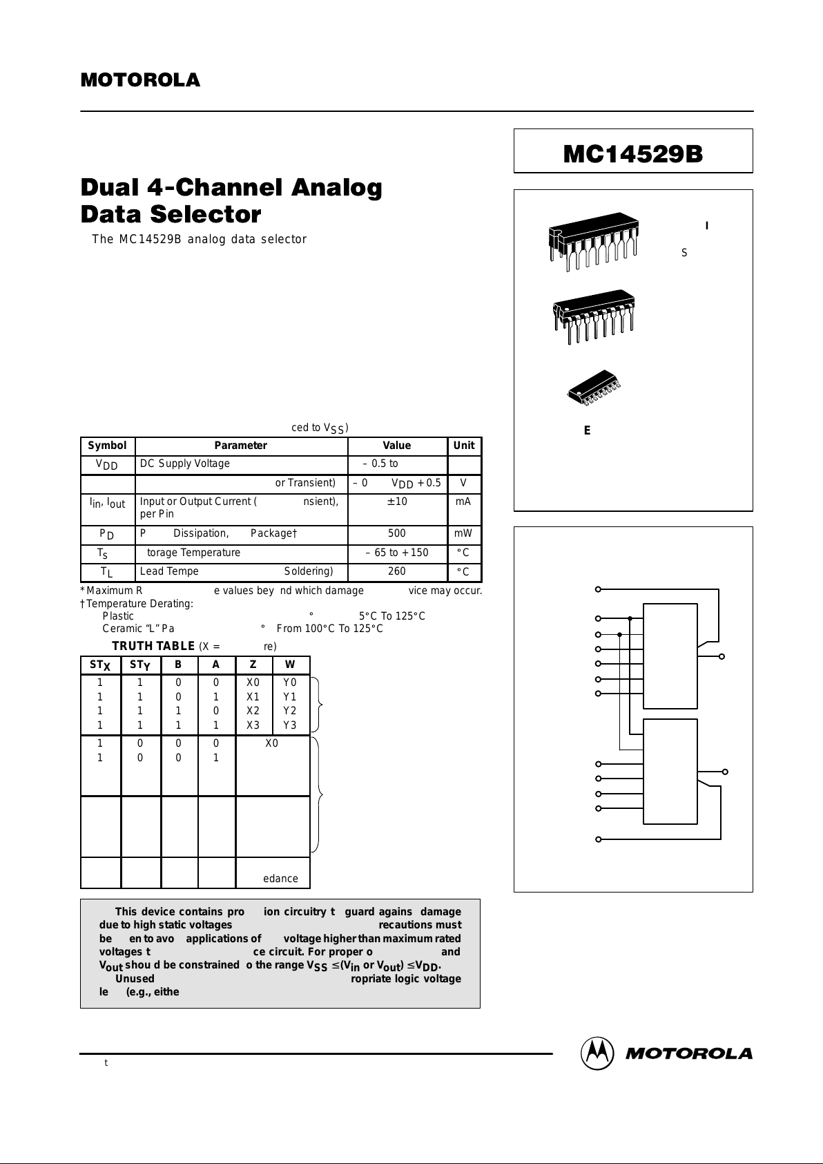
MC14529B
The MC14529B analog data selector is a dual 4–channel or single
8–channel device depending on the input coding. The device is suitable for
digital as well as analog application, including various one–of–four and
one–of–eight data selector functions. Since the device has bidirectional
analog characteristics it can also be used as a dual binary to 1–of–4 or a
binary to 1–of–8 decoder.
• Data Paths Are Bidirectional
• 3–State Outputs
• Linear “On” Resistance
• Supply Voltage Range = 3.0 Vdc to 18 Vdc
• Capable of Driving Two Low–power TTL Loads or One Low–power
Schottky TTL Load over the Rated Temperature Range.
MAXIMUM RATINGS* (Voltages Referenced to V
SS
)
Symbol
Parameter
Value
Unit
V
DD
DC Supply Voltage
– 0.5 to + 18.0
V
Vin, V
out
Input or Output Voltage (DC or Transient)
– 0.5 to VDD + 0.5
V
Iin, I
out
Input or Output Current (DC or Transient),
per Pin
± 10
mA
P
D
Power Dissipation, per Package†
500
mW
T
stg
Storage Temperature
– 65 to + 150
_
C
T
L
Lead Temperature (8–Second Soldering)
260
_
C
*Maximum Ratings are those values beyond which damage to the device may occur.
†Temperature Derating:
Plastic “P and D/DW” Packages: – 7.0 mW/_C From 65_C To 125_C
Ceramic “L” Packages: – 12 mW/_C From 100_C To 125_C
TRUTH TABLE (X = Don’t Care)
ST
X
ST
Y
B A Z W
1 1 0 0 X0 Y0
1 1 0 1 X1 Y1
1 1 1 0 X2 Y2
1 1 1 1 X3 Y3
1 0 0 0 X0
1 0 0 1 X1
1 0 1 0 X2
1 0 1 1 X3
0 1 0 0 Y0
0 1 0 1 Y1
0 1 1 0 Y2
0 1 1 1 Y3
0 0 X X High
Impedance
This device contains protection circuitry to guard against damage
due to high static voltages or electric fields. However, precautions must
be taken to avoid applications of any voltage higher than maximum rated
voltages to this high-impedance circuit. For proper operation, Vin and
V
out
should be constrained to the range VSS ≤ (Vin or V
out
) ≤ VDD.
Unused inputs must always be tied to an appropriate logic voltage
level (e.g., either VSS or VDD). Unused outputs must be left open.
Dual 4–Channel Mode
2 Outputs
Single 8–Channel Mode
1 Output
(Z and W tied together)
SEMICONDUCTOR TECHNICAL DATA
Motorola, Inc. 1995
REV 3
1/94
L SUFFIX
CERAMIC
CASE 620
ORDERING INFORMATION
MC14XXXBCP Plastic
MC14XXXBCL Ceramic
MC14XXXBD SOIC
TA = – 55° to 125°C for all packages.
P SUFFIX
PLASTIC
CASE 648
D SUFFIX
SOIC
CASE 751B
BLOCK DIAGRAM
VDD = PIN 16
VSS = PIN 8
10
9
Z
W
A
B
X0
X1
X2
X3
Y0
Y1
Y2
Y3
6
STROBE X 1
STROBE Y 15
7
2
3
4
5
14
13
12
11
3–STATE OUTPUT ENABLE
MOTOROLA CMOS LOGIC DATAMC14529B
2
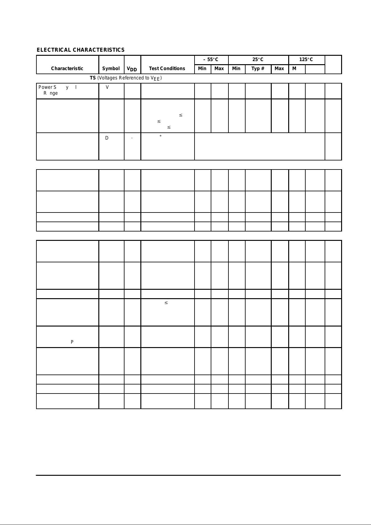
ELECTRICAL CHARACTERISTICS
– 55_C 25_C 125_C
Characteristic
Symbol
VDDTest Conditions
Min Max Min Typ # Max Min Max
Unit
SUPPLY REQUIREMENTS (Voltages Referenced to VEE)
Power Supply Voltage
Range
V
DD
— VDD – 3.0 ≥ VSS ≥
V
EE
3.0 18 3.0 — 18 3.0 18 V
Quiescent Current Per
Package
I
DD
5.0
10
15
Control Inputs: Vin =
VSS or VDD,
Switch I/O: VSS
v
V
I/O
v VDD, and
∆V
switch
v 500 mV**
—
—
—
1.0
1.0
2.0
—
—
—
0.005
0.010
0.015
1.0
1.0
2.0
—
—
—
60
60
120
µA
Total Supply Current
(Dynamic Plus
Quiescent, Per Package
I
D(AV)
5.0
10
15
TA = 25_C only (The
channel component,
(Vin – V
out
)/Ron, is
not included.)
(0.07 µA/kHz) f + I
DD
Typical (0.20 µA/kHz) f + I
DD
(0.36 µA/kHz) f + I
DD
µA
CONTROL INPUTS — INHIBIT, A, B (Voltages Referenced to VSS)
Low–Level Input Voltage V
IL
5.0
10
15
Ron = per spec,
I
off
= per spec
—
—
—
1.5
3.0
4.0
—
—
—
2.25
4.50
6.75
1.5
3.0
4.0
—
—
—
1.5
3.0
4.0
V
High–Level Input Voltage V
IH
5.0
10
15
Ron = per spec,
I
off
= per spec
3.5
7.0
11
—
—
—
3.5
7.0
11
2.75
5.50
8.25
—
—
—
3.5
7.0
11
—
—
—
V
Input Leakage Current I
in
15 Vin = 0 or V
DD
— ± 0.1 — ±0.00001 ±0.1 — ±1.0 µA
Input Capacitance C
in
— — — — 5.0 7.5 — — pF
SWITCHES IN/OUT AND COMMONS OUT/IN — W, Z (Voltages Referenced to VEE)
Recommended Peak–to–
Peak Voltage Into or
Out of the Switch
V
I/O
— Channel On or Off 0 V
DD
0 — V
DD
0 V
DDVp–p
Recommended Static or
Dynamic Voltage
Across the Switch**
(Figure 5)
∆V
switch
— Channel On 0 600 0 — 600 0 300 mV
Output Offset Voltage V
OO
— Vin = 0 V, No Load — — — 10 — — — µV
ON Resistance R
on
1015∆V
switch
v 500 mV**,
Vin = VIL or V
IH
(Control), and Vin =
0 to VDD (Switch)
——400
240——
120
80
480
270——
560
350
Ω
∆ON Resistance Between
Any Two Channels
in the Same Package
∆R
on
10
15
—————
—
15
10
———
—
—
—
Ω
Off–Channel Leakage
Current (Figure 10)
I
off
15 Vin = VIL or V
IH
(Control) Channel to
Channel or Any One
Channel
± 100 — ± 0.05 ± 100 — ±1000 nA
Capacitance, Switch I/O C
I/O
— Inhibit = V
DD
— — — 8.0 — — — pF
Capacitance, Common O/I C
O/I
— Inhibit = V
DD
— — — 20 — — — pF
Capacitance, Feedthrough
(Channel Off)
C
I/O
——Pins Not Adjacent
Pins Adjacent
—————
—
0.15
0.47
———
—
—
—
pF
#Data labelled “Typ” is not to be used for design purposes, but is intended as an indication of the IC’s potential performance.
** For voltage drops across the switch (∆V
switch
) > 600 mV ( > 300 mV at high temperature), excessive VDD current may be drawn; i.e. the
current out of the switch may contain both VDD and switch input components. The reliability of the device will be unaffected unless the Maximum
Ratings are exceeded. (See first page of this data sheet.)
MOTOROLA CMOS LOGIC DATA
3
MC14529B
SWTCHING CHARACTERISTICS (T
A
= 25_C)
Characteristic
Figure Symbol V
SS
V
DD
Min Typ # Max Unit
Vin to V
out
Propagation Delay Time
(CL = 50 pF, RL = 1.0 kΩ)
7 t
PLH
, t
PHL
0.0 5.0
10
15
—
—
—
20
10
8.0
40
20
15
ns
Propagation Delay Time, Control to
Output, Vin = VDD or V
SS
(CL = 50 pF, RL = 1.0 kΩ)
8 t
PLZ
, t
PZL
,
t
PHZ
, t
PZH
0.0 5.0
10
15
—
—
—
140
70
50
400
160
120
ns
Crosstalk, Control to Output
(CL = 50 pF, RL = 1.0 kΩ
R
out
= 10 kΩ)
9 — 0.0 5.0
10
15
—
—
—
5.0
5.0
5.0
—
—
mV
Control Input Pulse Frequency
(CL = 50 pF, RL = 1.0 kΩ)
10 f
in
0.0 5.0
10
15
—
—
—
5.0
10
12
2.5
6.2
8.3
MHz
Noise Voltage
(f = 100 Hz)
11, 12 — 0.0 5.0
10
15
5.0
10
15
—
—
—
—
—
—
24
25
30
12
12
15
—
—
—
—
—
—
nV/
√cycle
Sine Wave Distortion
(Vin = 1.77 Vdc RMS
Centered @ 0.0 Vdc,
RL = 10 kΩ, f = 1.0 kHz)
— — – 5.0 5.0 — 0.36 — %
Off–Channel Leakage Current
(Vin = + 5.0 Vdc, V
out
= – 5.0 Vdc)
(Vin = – 5.0 Vdc, V
out
= + 5.0 Vdc)
(Vin = + 7.5 Vdc, V
out
= – 7.5 Vdc)
(Vin = – 7.5 Vdc, V
out
= + 7.5 Vdc)
— I
off
– 5.0
– 5.0
– 7.5
– 7.5
5.0
5.0
7.5
7.5
—
—
—
—
± 0.001
± 0.001
± 0.0015
± 0.0015
± 125
± 125
± 250
± 250
nA
Insertion Loss
(Vin = 1.77 Vdc
RMS centered @ 0.0 Vdc,
f = 1.0 MHz)
I
loss
= 20 Log10 (V
out/Vin
)
(RL = 1.0 kΩ)
(RL = 10 kΩ)
(RL = 100 kΩ)
(RL = 1.0 MΩ)
13 — – 5.0 5.0
—
—
—
—
2.0
0.8
0.25
0.01
—
—
—
—
dB
Bandwidth (– 3 dB)
(Vin = 1.77 Vdc
RMS centered @ 0.0 Vdc)
(RL = 1.0 kΩ)
(RL = 10 kΩ)
(RL = 100 kΩ)
(RL = 1.0 MΩ)
— BW – 5.0 5.0
—
—
—
—
35
28
27
26
—
—
—
—
MHz
Feedthrough and Crosstalk
20 Log10 (V
out/Vin
) = – 50 dB
(RL = 1.0 kΩ)
(RL = 10 kΩ)
(RL = 100 kΩ)
(RL = 1.0 MΩ)
— — – 5.0 5.0
—
—
—
—
850
100
12
1.5
—
—
—
—
MHz
#Data labelled “Typ” is not to be used for design purposes but is intended as an indication of the IC’s potential performance.

MOTOROLA CMOS LOGIC DATAMC14529B
4
Figure 1. Output Voltage
Test Circuit
Figure 2. Noise Immunity
Test Circuit
Pins 2, 3, 4, 12, 13 and 14 are left open.
VIL: VC is raised from VSS until VC = VIL.
VIL: at VC = VIL: IS = ± 10 µA with Vin = VSS, V
out
= V
DD
VIL: Vin = VDD, V
out
= VSS.
VIH: When VC = VIH to VDD, the switch is ON and the R
ON
VIH: specifications are met.
V
V
DD
V
in
VSS = 0.0 V
V
SS
OUT
V
N
1 k
V
DD
V
SS
I
S
Z
W
ST
X
ST
Y
A
B
X3
Y3
Figure 3. Quiescent Power Dissipation
Test Circuit
Figure 4. RON Characteristics
Test Circuit
PULSE
GENERATOR
V
DD
OUT
10 k
V
SS
V
in
I
D
V
DD
f
c
A0, A1
PD = VDD x I
D
V
DD
OUT
V
SS
V
in
R
L
STX = STY = V
DD
TYPICAL RON versus INPUT VOLTAGE
Figure 5. Figure 6.
Vin, INPUT VOLTAGE (Vdc) Vin, INPUT VOLTAGE (Vdc)
–10 –5 0 5 10 0 5 10 15 20 25
VDD = 15 V
VSS = 0 V
VDD = 10 V
VSS = 0 V
VDD = 5 V
VSS = –5 V
VDD = 7.5 V
VSS = –7.5 V
R “ON” RESISTANCE (OHMS)
ON
R “ON” RESISTANCE (OHMS)
ON
250
200
150
100
50
0
250
200
150
100
50
0

MOTOROLA CMOS LOGIC DATA
5
MC14529B
Figure 7. Propagation Delay Test Circuit
and Waveforms
Figure 8. Turn–On Delay Time Test Circuit
and Waveforms
V
DD
V
SS
50%
20 ns
10%
90%
50%
20 ns
t
PHL
t
PLH
V
SS
V
in
V
out
V
in
V
DD
C
L
R
L
OUT
V
DD
V
SS
V
SS
V
DD
V
DD
V
SS
C
L
10%
90%
t
PZL
t
PLZ
20 ns
R
L
V
out
V
in
10%
V
out
V
out
90%
10%
50%
V
X
90%
V
in
V
x
V
in
V
x
t
PHZ
t
PZH
STX, ST
Y
STX, ST
Y
Figure 9. Crosstalk Test Circuit Figure 10. Frequency Response Test Circuit
A OR B
CONTROL
LOGIC
10 k
50 pF
OUT
V
in
1 k
R
L
V
DD
OUT
X, Y INPUT
V
SS
V
DD
V
SS
V
Feedthrough
R
L
X, Y
INPUT
+2.5 Vdc
–2.5 Vdc
0.0 Vdc
V
in
Figure 11. Noise Voltage Test Circuit Figure 12. Typical Noise Characteristics
QUAN–TECH
MODEL
2283
OR EQUIV
V
DD
V
SS
OUT
IN
35
30
25
20
15
10
5.0
0
10 100 1.0 k 10 k 100 k
VDD = 15 Vdc
5.0 Vdc
10 Vdc
f, FREQUENCY (Hz)
NOISE VOLTAGE (nV/ CYCLE)
p

MOTOROLA CMOS LOGIC DATAMC14529B
6
Figure 13. Typical Insertion Loss/Bandwidth
Characteristics
PIN ASSIGNMENT
13
14
15
16
9
10
11
125
4
3
2
1
8
7
6
Y2
Y1
Y0
ST
Y
V
DD
Z
W
Y3
X2
X1
X0
ST
X
V
SS
B
A
X3
10 k 100 k 1.0 M 10 M 100 M
2.0
0
–2.0
–4.0
–6.0
–8.0
–10
–12
fin, INPUT FREQUENCY (Hz)
TYPICAL INSERTION LOSS (dB)
RL = 1 MW AND 100 k
W
1.0 k
W
10 k
W
–3.0 dB (RL = 1.0 M
W)
–3.0 dB (RL = 10 k
W)
–3.0 dB (RL = 1.0 k
W)
LOGIC DIAGRAM
VDD = PIN 16
VSS = PIN 8
11
12
5
4
3
2
13
14
10
W
9
Z
Y3
Y2
Y1
Y0
X3
X2
X1
X0
15 167
STYST
X
AB

MOTOROLA CMOS LOGIC DATA
7
MC14529B
OUTLINE DIMENSIONS
P SUFFIX
PLASTIC DIP PACKAGE
CASE 648–08
ISSUE R
NOTES:
1. DIMENSIONING AND TOLERANCING PER ANSI
Y14.5M, 1982.
2. CONTROLLING DIMENSION: INCH.
3. DIMENSION L TO CENTER OF LEADS WHEN
FORMED PARALLEL.
4. DIMENSION B DOES NOT INCLUDE MOLD FLASH.
5. ROUNDED CORNERS OPTIONAL.
–A–
B
F
C
S
H
G
D
J
L
M
16 PL
SEATING
1 8
916
K
PLANE
–T–
M
A
M
0.25 (0.010) T
DIM MIN MAX MIN MAX
MILLIMETERSINCHES
A 0.740 0.770 18.80 19.55
B 0.250 0.270 6.35 6.85
C 0.145 0.175 3.69 4.44
D 0.015 0.021 0.39 0.53
F 0.040 0.70 1.02 1.77
G 0.100 BSC 2.54 BSC
H 0.050 BSC 1.27 BSC
J 0.008 0.015 0.21 0.38
K 0.110 0.130 2.80 3.30
L 0.295 0.305 7.50 7.74
M 0 10 0 10
S 0.020 0.040 0.51 1.01
____
L SUFFIX
CERAMIC DIP PACKAGE
CASE 620–10
ISSUE V
NOTES:
1. DIMENSIONING AND TOLERANCING PER
ANSI Y14.5M, 1982.
2. CONTROLLING DIMENSION: INCH.
3. DIMENSION L TO CENTER OF LEAD WHEN
FORMED PARALLEL.
4. DIMENSION F MAY NARROW TO 0.76 (0.030)
WHERE THE LEAD ENTERS THE CERAMIC
BODY.
–A–
–B–
–T–
F
E
G
N
K
C
SEATING
PLANE
16 PLD
S
A
M
0.25 (0.010) T
16 PLJ
S
B
M
0.25 (0.010) T
M
L
DIM MIN MAX MIN MAX
MILLIMETERSINCHES
A 0.750 0.785 19.05 19.93
B 0.240 0.295 6.10 7.49
C ––– 0.200 ––– 5.08
D 0.015 0.020 0.39 0.50
E 0.050 BSC 1.27 BSC
F 0.055 0.065 1.40 1.65
G 0.100 BSC 2.54 BSC
H 0.008 0.015 0.21 0.38
K 0.125 0.170 3.18 4.31
L 0.300 BSC 7.62 BSC
M 0 15 0 15
N 0.020 0.040 0.51 1.01
_ _ _ _
16 9
1 8

MOTOROLA CMOS LOGIC DATAMC14529B
8
OUTLINE DIMENSIONS
D SUFFIX
PLASTIC SOIC PACKAGE
CASE 751B–05
ISSUE J
NOTES:
1. DIMENSIONING AND TOLERANCING PER ANSI
Y14.5M, 1982.
2. CONTROLLING DIMENSION: MILLIMETER.
3. DIMENSIONS A AND B DO NOT INCLUDE
MOLD PROTRUSION.
4. MAXIMUM MOLD PROTRUSION 0.15 (0.006)
PER SIDE.
5. DIMENSION D DOES NOT INCLUDE DAMBAR
PROTRUSION. ALLOWABLE DAMBAR
PROTRUSION SHALL BE 0.127 (0.005) TOTAL
IN EXCESS OF THE D DIMENSION AT
MAXIMUM MATERIAL CONDITION.
1 8
16 9
SEATING
PLANE
F
J
M
R
X 45
_
G
8 PLP
–B–
–A–
M
0.25 (0.010) B
S
–T–
D
K
C
16 PL
S
B
M
0.25 (0.010) A
S
T
DIM MIN MAX MIN MAX
INCHESMILLIMETERS
A 9.80 10.00 0.386 0.393
B 3.80 4.00 0.150 0.157
C 1.35 1.75 0.054 0.068
D 0.35 0.49 0.014 0.019
F 0.40 1.25 0.016 0.049
G 1.27 BSC 0.050 BSC
J 0.19 0.25 0.008 0.009
K 0.10 0.25 0.004 0.009
M 0 7 0 7
P 5.80 6.20 0.229 0.244
R 0.25 0.50 0.010 0.019
_ _ _ _
How to reach us:
USA/EUROPE/Locations Not Listed: Motorola Literature Distribution; JAPAN: Nippon Motorola Ltd.; Tatsumi–SPD–JLDC, 6F Seibu–Butsuryu–Center,
P.O. Box 20912; Phoenix, Arizona 85036. 1–800–441–2447 or 602–303–5454 3–14–2 Tatsumi Koto–Ku, Tokyo 135, Japan. 03–81–3521–8315
MFAX: RMFAX0@email.sps.mot.com – TOUCHTONE 602–244–6609 ASIA/PACIFIC: Motorola Semiconductors H.K. Ltd.; 8B Tai Ping Industrial Park,
INTERNET: http://Design–NET.com 51 Ting Kok Road, Tai Po, N.T., Hong Kong. 852–26629298
Motorola reserves the right to make changes without further notice to any products herein. Motorola makes no warranty , representation or guarantee regarding
the suitability of its products for any particular purpose, nor does Motorola assume any liability arising out of the application or use of any product or circuit,
and specifically disclaims any and all liability, including without limitation consequential or incidental damages. “Typical” parameters which may be provided
in Motorola data sheets and/or specifications can and do vary in different applications and actual performance may vary over time. All operating parameters,
including “Typicals” must be validated for each customer application by customer’s technical experts. Motorola does not convey any license under its patent
rights nor the rights of others. Motorola products are not designed, intended, or authorized for use as components in systems intended for surgical implant
into the body, or other applications intended to support or sustain life, or for any other application in which the failure of the Motorola product could create a
situation where personal injury or death may occur. Should Buyer purchase or use Motorola products for any such unintended or unauthorized application,
Buyer shall indemnify and hold Motorola and its officers, employees, subsidiaries, affiliates, and distributors harmless against all claims, costs, damages, and
expenses, and reasonable attorney fees arising out of, directly or indirectly, any claim of personal injury or death associated with such unintended or
unauthorized use, even if such claim alleges that Motorola was negligent regarding the design or manufacture of the part. Motorola and are registered
trademarks of Motorola, Inc. Motorola, Inc. is an Equal Opportunity/Affirmative Action Employer .
MC14529B/D
*MC14529B/D*
◊
 Loading...