

Motorola MC14517BDW, MC14517BCL, MC14517BCP Datasheet
MOTOROLA CMOS LOGIC DATA
403
MC14517B
The MC14517B dual 64–bit static shift register consists of two identical,
independent, 64–bit registers. Each register has separate clock and write
enable inputs, as well as outputs at bits 16, 32, 48, and 64. Data at the data
input is entered by clocking, regardless of the state of the write enable input.
An output is disabled (open circuited) when the write enable input is high.
During this time, data appearing at the data input as well as the 16–bit,
32–bit, and 48–bit taps may be entered into the device by application of a
clock pulse. This feature permits the register to be loaded with 64 bits in 16
clock periods, and also permits bus logic to be used. This device is useful in
time delay circuits, temporary memory storage circuits, and other serial shift
register applications.
• Diode Protection on All Inputs
• Fully Static Operation
• Output Transitions Occur on the Rising Edge of the Clock Pulse
• Exceedingly Slow Input Transition Rates May Be Applied to the Clock
Input
• 3–State Output at 64th–Bit Allows Use in Bus Logic Applications
• Shift Registers of any Length may be Fully Loaded with 16 Clock Pulses
• Supply Voltage Range = 3.0 Vdc to 18 Vdc
• Capable of Driving Two Low–power TTL Loads or One Low–power
Schottky TTL Load Over the Rated Temperature Range
MAXIMUM RATINGS (Voltages referenced to V
SS
)
Symbol
Parameter
Value
Unit
V
DD
DC Supply Voltage
– 0.5 to + 18.0
V
Vin, V
out
Input or Output Voltage (DC or Transient)
– 0.5 to VDD + 0.5
V
Iin, I
out
Input or Output Current (DC or Transient),
per Pin
± 10
mA
P
D
Power Dissipation, per Package†
500
mW
T
stg
Storage Temperature
– 65 to + 150
_
C
T
L
Lead Temperature (8–Second Soldering)
260
_
C
*Maximum Ratings are those values beyond which damage to the device may occur.
†Temperature Derating:
Plastic “P and D/DW” Packages: – 7.0 mW/_C From 65_C To 125_C
Ceramic “L” Packages: – 12 mW/_C From 100_C To 125_C
FUNCTIONAL TRUTH TABLE (X = Don’t Care)
Clock
Write
Enable
Data 16–Bit Tap 32–Bit Tap 48–Bit Tap 64–Bit Tap
0 0 X Content of 16–Bit
Displayed
Content of 32–Bit
Displayed
Content of 48–Bit
Displayed
Content of 64–Bit
Displayed
0 1 X High Impedance High Impedance High Impedance High Impedance
1 0 X Content of 16–Bit
Displayed
Content of 32–Bit
Displayed
Content of 48–Bit
Displayed
Content of 64–Bit
Displayed
1 1 X High Impedance High Impedance High Impedance High Impedance
0 Data entered
into 1st Bit
Content of 16–Bit
Displayed
Content of 32–Bit
Displayed
Content of 48–Bit
Displayed
Content of 64–Bit
Displayed
1 Data entered
into 1st Bit
Data at tap
entered into 17–Bit
Data at tap
entered into 33–Bit
Data at tap
entered into 49–Bit
High Impedance
0 X Content of 16–Bit
Displayed
Content of 32–Bit
Displayed
Content of 48–Bit
Displayed
Content of 64–Bit
Displayed
1 X High Impedance High Impedance High Impedance High Impedance
SEMICONDUCTOR TECHNICAL DATA
Motorola, Inc. 1995
REV 3
1/94
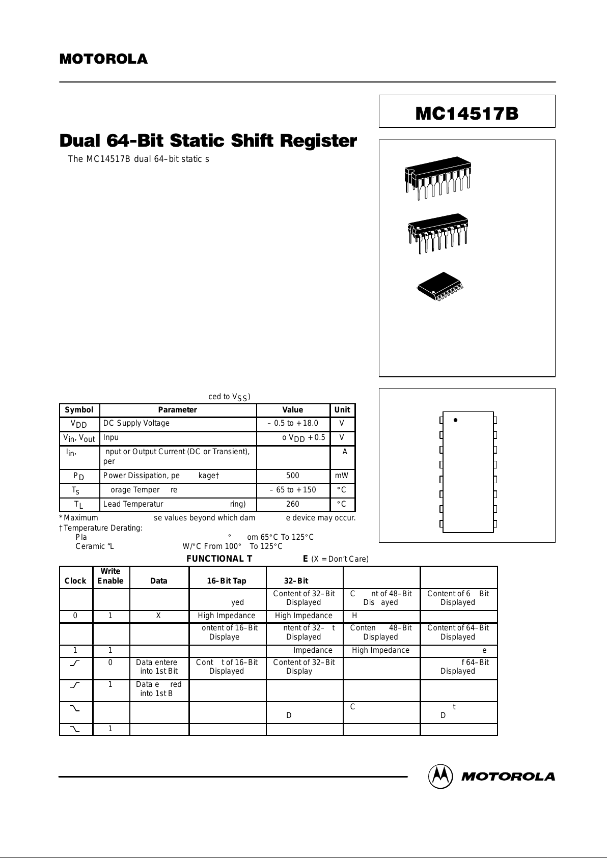
L SUFFIX
CERAMIC
CASE 620
ORDERING INFORMATION
MC14XXXBCP Plastic
MC14XXXBCL Ceramic
MC14XXXBDW SOIC
TA = – 55° to 125°C for all packages.
P SUFFIX
PLASTIC
CASE 648
DW SUFFIX
SOIC
CASE 751G
PIN ASSIGNMENT
13
14
15
16
9
10
11
125
4
3
2
1
8
7
6
C
B
WE
B
Q48
B
Q16
B
V
DD
D
B
Q32
B
Q64
B
C
A
WE
A
Q48
A
Q16
A
V
SS
Q32
A
Q64
A
D
A
MOTOROLA CMOS LOGIC DATAMC14517B
404
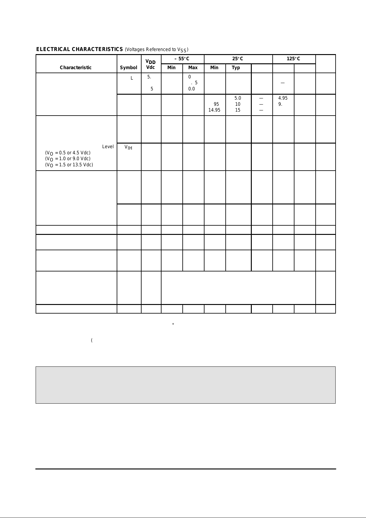
ELECTRICAL CHARACTERISTICS (Voltages Referenced to V
SS
)
V
– 55_C 25_C 125_C
Characteristic
Symbol
V
DD
Vdc
Min Max Min Typ # Max Min Max
Unit
Output Voltage
“0” Level
Vin = VDD or 0
V
OL
5.0
10
15
—
—
—
0.05
0.05
0.05
—
—
—
0
0
0
0.05
0.05
0.05
—
—
—
0.05
0.05
0.05
Vdc
“1” Level
Vin = 0 or V
DD
V
OH
5.0
10
15
4.95
9.95
14.95
—
—
—
4.95
9.95
14.95
5.0
10
15
—
—
—
4.95
9.95
14.95
—
—
—
Vdc
Input Voltage
“0” Level
(VO = 4.5 or 0.5 Vdc)
(VO = 9.0 or 1.0 Vdc)
(VO = 13.5 or 1.5 Vdc)
V
IL
5.0
10
15
—
—
—
1.5
3.0
4.0
—
—
—
2.25
4.50
6.75
1.5
3.0
4.0
—
—
—
1.5
3.0
4.0
Vdc
“1” Level
(VO = 0.5 or 4.5 Vdc)
(VO = 1.0 or 9.0 Vdc)
(VO = 1.5 or 13.5 Vdc)
V
IH
5.0
10
15
3.5
7.0
11
—
—
—
3.5
7.0
11
2.75
5.50
8.25
—
—
—
3.5
7.0
11
—
—
—
Vdc
Output Drive Current
(VOH = 2.5 Vdc) Source
(VOH = 4.6 Vdc)
(VOH = 9.5 Vdc)
(VOH = 13.5 Vdc)
I
OH
5.0
5.0
10
15
– 3.0
– 0.64
– 1.6
– 4.2
—
—
—
—
– 2.4
– 0.51
– 1.3
– 3.4
– 4.2
– 0.88
– 2.25
– 8.8
—
—
—
—
– 1.7
– 0.36
– 0.9
– 2.4
—
—
—
—
mAdc
(VOL = 0.4 Vdc) Sink
(VOL = 0.5 Vdc)
(VOL = 1.5 Vdc)
I
OL
5.0
10
15
0.64
1.6
4.2
—
—
—
0.51
1.3
3.4
0.88
2.25
8.8
—
—
—
0.36
0.9
2.4
—
—
—
mAdc
Input Current I
in
15 — ± 0.1 — ±0.00001 ± 0.1 — ± 1.0 µAdc
Input Capacitance
(Vin = 0)
C
in
— — — — 5.0 7.5 — — pF
Quiescent Current
(Per Package)
I
DD
5.0
10
15
—
—
—
5.0
10
20
—
—
—
0.005
0.010
0.015
5.0
10
20
—
—
—
150
300
600
µAdc
Total Supply Current**†
(Dynamic plus Quiescent,
Per Package)
(CL = 50 pF on all outputs, all
buffers switching)
I
T
5.0
10
15
IT = (4.2 µA/kHz) f + I
DD
IT = (8.8 µA/kHz) f + I
DD
IT = (13.7 µA/kHz) f + I
DD
µAdc
Three–State Leakage Current I
TL
15 — ± 0.1 — ± 0.0001 ± 0.1 — ± 3.0 µAdc
#Data labelled “Typ” is not to be used for design purposes but is intended as an indication of the IC’s potential performance.
**āThe formulas given are for the typical characteristics only at 25_C.
†To calculate total supply current at loads other than 50 pF:
IT(CL) = IT(50 pF) + (CL – 50) Vfk
where: IT is in µA (per package), CL in pF, V = (VDD – VSS) in volts, f in kHz is input frequency, and k = 0.004.
This device contains protection circuitry to guard against damage due to high static voltages or electric fields. However,
precautions must be taken to avoid applications of any voltage higher than maximum rated voltages to this high-impedance
circuit. For proper operation, Vin and V
out
should be constrained to the range VSS ≤ (Vin or V
out
) ≤ VDD.
Unused inputs must always be tied to an appropriate logic voltage level (e.g., either VSS or VDD). Unused outputs must
be left open.
 Loading...