

MC14517B
Dual 64-Bit Static Shift
Register
The MC14517B dual 64–bit static shift register consists of two
identical, independent, 64–bit registers. Each register has separate clock
and write enable inputs, as well as outputs at bits 16, 32, 48, and 64. Data
at the data input is entered by clocking, regardless of the state of the write
enable input. An output is disabled (open circuited) when the write enable
input is high. During this time, data appearing at the data input as well as
the 16–bit, 32–bit, and 48–bit taps may be entered into the device by
application of a clock pulse. This feature permits the register to be loaded
with 64 bits in 16 clock periods, and also permits bus logic to be used.
This device is useful in time delay circuits, temporary memory storage
circuits, and other serial shift register applications.
• Diode Protection on All Inputs
• Fully Static Operation
• Output Transitions Occur on the Rising Edge of the Clock Pulse
• Exceedingly Slow Input Transition Rates May Be Applied to the
Clock Input
• 3–State Output at 64th–Bit Allows Use in Bus Logic Applications
• Shift Registers of any Length may be Fully Loaded with 16 Clock
Pulses
• Supply Voltage Range = 3.0 Vdc to 18 Vdc
• Capable of Driving T wo Low–power TTL Loads or One Low–power
Schottky TTL Load Over the Rated T emperature Range
http://onsemi.com
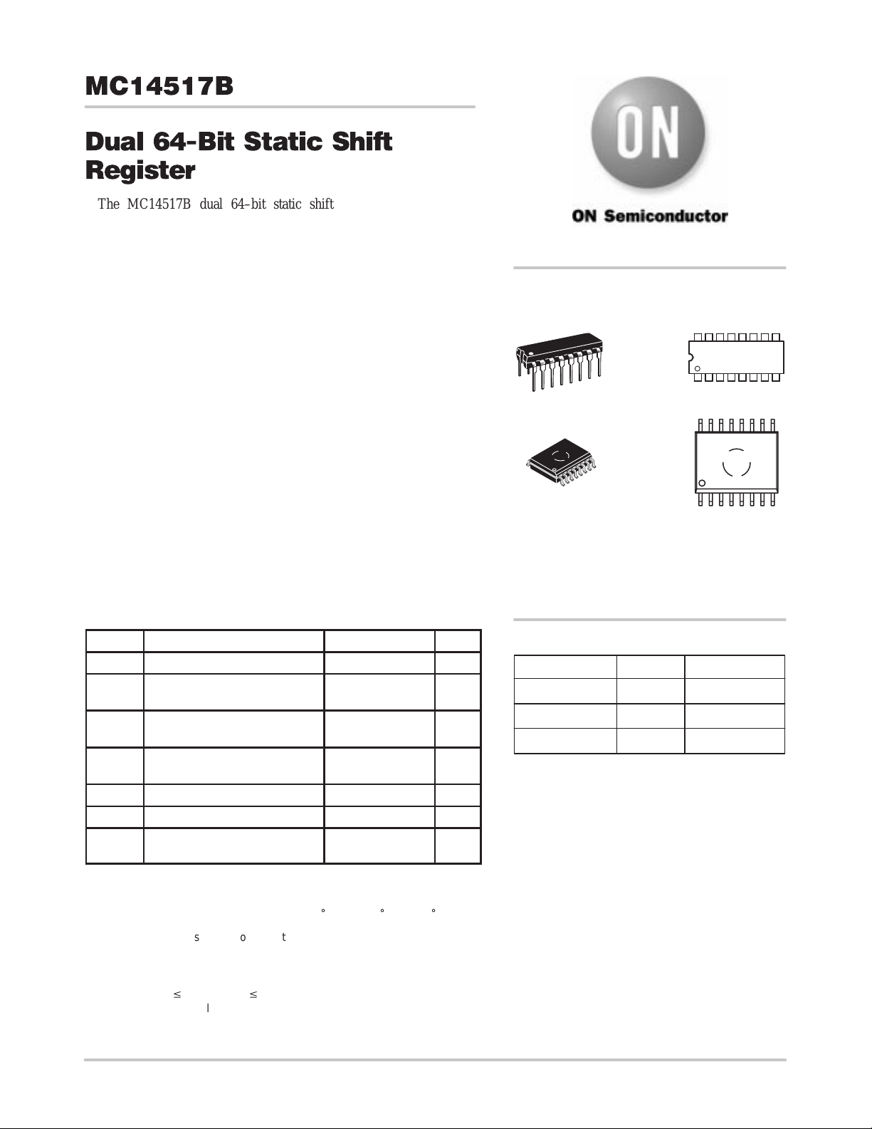
MARKING
DIAGRAMS
16
PDIP–16
P SUFFIX
CASE 648
SOIC–16
DW SUFFIX
CASE 751G
A = Assembly Location
WL or L = Wafer Lot
YY or Y = Year
WW or W = Work Week
MC14517BCP
AWLYYWW
1
16
AWLYYWW
1
14517B
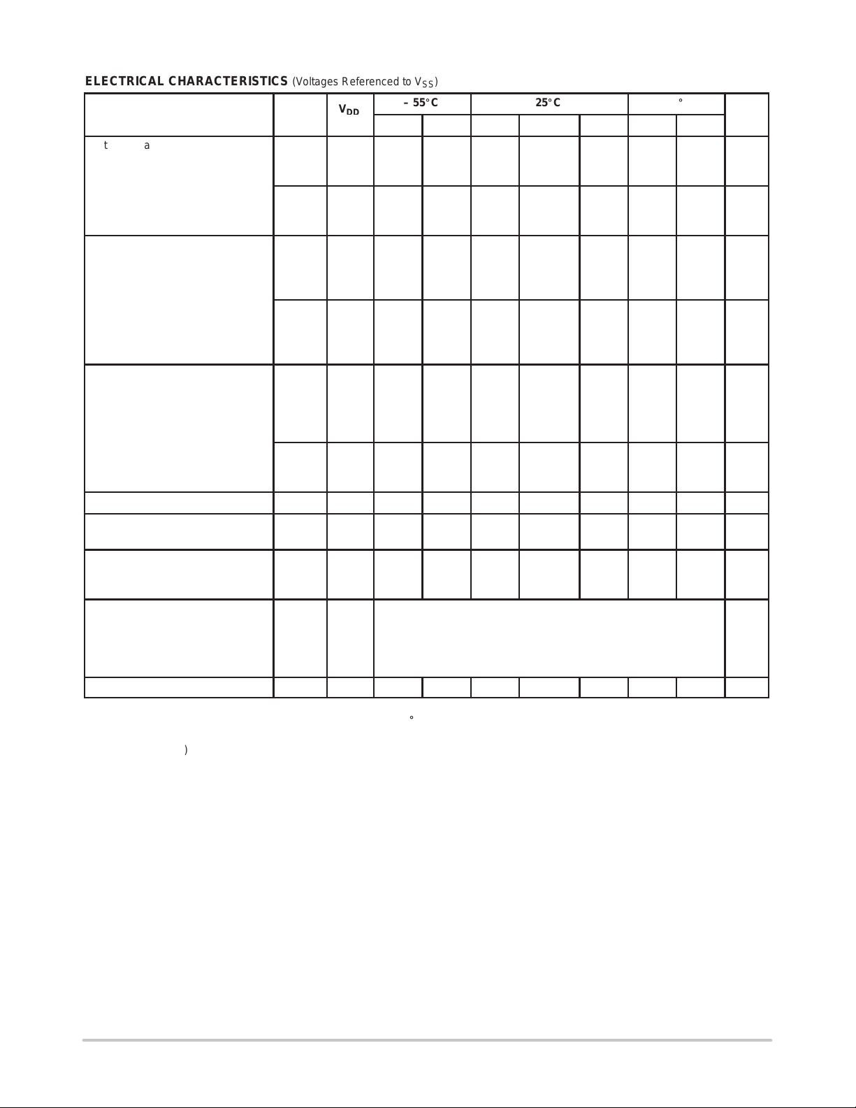
MAXIMUM RATINGS (Voltages Referenced to V
Symbol
V
DD
Vin, V
Iin, I
P
T
T
stg
T
1. Maximum Ratings are those values beyond which damage to the device
may occur.
2. Temperature Derating:
Plastic “P and D/DW” Packages: – 7.0 mW/_C From 65_C To 125_C
This device contains protection circuitry to guard against damage due to high
static voltages or electric fields. However, precautions must be taken to avoid
applications of any voltage higher than maximum rated voltages to this
high–impedance circuit. For proper operation, V
to the range V
Unused inputs must always be tied to an appropriate logic voltage level (e.g.,
either V
DC Supply Voltage Range –0.5 to +18.0 V
Input or Output Voltage Range
out
Input or Output Current
out
Power Dissipation,
D
Operating Temperature Range –55 to +125 °C
A
Storage Temperature Range –65 to +150 °C
Lead Temperature
L
SS
or VDD). Unused outputs must be left open.
SS
Parameter Value Unit
(DC or Transient)
(DC or Transient) per Pin
per Package (Note 2.)
(8–Second Soldering)
v (Vin or V
) v VDD.
out
) (Note 1.)
SS
–0.5 to VDD + 0.5 V
±10 mA
500 mW
260 °C
and V
in
should be constrained
out
ORDERING INFORMATION
Device Package Shipping
MC14517BCP PDIP–16 2000/Box
MC14517BDW SOIC–16 47/Rail
MC14517BDWR2 SOIC–16 1000/Tape & Reel
Semiconductor Components Industries, LLC, 2000
March, 2000 – Rev . 3
1 Publication Order Number:
MC14517B/D
MC14517B
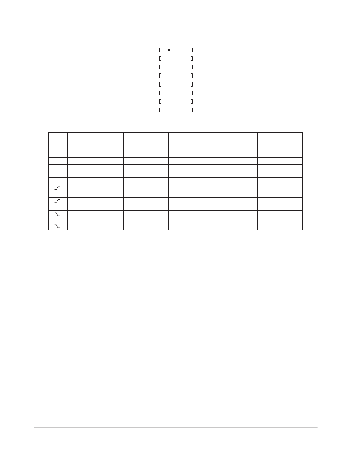
PIN ASSIGNMENT
Q16
Q48
WE
Q64
Q32
V
1
A
2
A
3
A
C
4
A
A
6
A
D
7
A
8
SS
16
V
DD
15
Q16
B
Q48
14
13
125
11
10
B
WE
B
C
B
Q64
B
Q32
B
D
9
B
FUNCTIONAL TRUTH TABLE (X = Don’t Care)
Write
Clock
Enable
0 0 X Content of 16–Bit
Data 16–Bit Tap 32–Bit Tap 48–Bit Tap 64–Bit Tap
Displayed
Content of 32–Bit
Displayed
Content of 48–Bit
Displayed
Content of 64–Bit
Displayed
0 1 X High Impedance High Impedance High Impedance High Impedance
1 0 X Content of 16–Bit
Displayed
Content of 32–Bit
Displayed
Content of 48–Bit
Displayed
Content of 64–Bit
Displayed
1 1 X High Impedance High Impedance High Impedance High Impedance
0 Data entered
into 1st Bit
1 Data entered
into 1st Bit
0 X Content of 16–Bit
Content of 16–Bit
Displayed
Data at tap
entered into 17–Bit
Displayed
Content of 32–Bit
Displayed
Data at tap
entered into 33–Bit
Content of 32–Bit
Displayed
Content of 48–Bit
Displayed
Data at tap
entered into 49–Bit
Content of 48–Bit
Displayed
Content of 64–Bit
Displayed
High Impedance
Content of 64–Bit
Displayed
1 X High Impedance High Impedance High Impedance High Impedance
http://onsemi.com
2
MC14517B
V
DD
ELECTRICAL CHARACTERISTICS (Voltages Referenced to V
V
Characteristic Symbol
Output Voltage “0” Level
= VDD or 0
V
in
“1” Level
V
= 0 or V
in
DD
Input Voltage “0” Level
(V
= 4.5 or 0.5 Vdc)
O
= 9.0 or 1.0 Vdc)
(V
O
(V
= 13.5 or 1.5 Vdc)
O
“1” Level
= 0.5 or 4.5 Vdc)
(V
O
(V
= 1.0 or 9.0 Vdc)
O
= 1.5 or 13.5 Vdc)
(V
O
Output Drive Current
(V
= 2.5 Vdc) Source
OH
= 4.6 Vdc)
(V
OH
(V
= 9.5 Vdc)
OH
(V
= 13.5 Vdc)
OH
(VOL = 0.4 Vdc) Sink
(V
= 0.5 Vdc)
OL
(V
= 1.5 Vdc)
OL
Input Current I
Input Capacitance
(V
= 0)
in
Quiescent Current
(Per Package)
Total Supply Current
(4.) (5.)
(Dynamic plus Quiescent,
Per Package)
= 50 pF on all outputs, all
(C
L
V
OL
V
OH
V
V
I
OH
I
OL
in
C
I
DD
I
Vdc
5.0
10
15
5.0
10
15
IL
5.0
10
15
IH
5.0
10
15
5.0
5.0
10
15
5.0
10
15
Min Max Min Typ
—
—
—
4.95
9.95
14.95
—
—
—
3.5
7.0
11
– 3.0
– 0.64
– 1.6
– 4.2
0.64
1.6
4.2
15 — ± 0.1 — ±0.00001 ± 0.1 — ± 1.0 µAdc
in
T
— — — — 5.0 7.5 — — pF
5.0
10
15
—
—
—
5.0
10
15
)
SS
– 55_C 25_C 125_C
(3.)
Max Min Max
0.05
0.05
0.05
—
—
—
1.5
3.0
4.0
—
—
—
—
—
—
—
—
—
—
5.0
10
20
—
—
—
4.95
9.95
14.95
—
—
—
3.5
7.0
11
– 2.4
– 0.51
– 1.3
– 3.4
0.51
1.3
3.4
—
—
—
0
0
0
5.0
10
15
2.25
4.50
6.75
2.75
5.50
8.25
– 4.2
– 0.88
– 2.25
– 8.8
0.88
2.25
8.8
0.005
0.010
0.015
IT = (4.2 µA/kHz) f + I
IT = (8.8 µA/kHz) f + I
IT = (13.7 µA/kHz) f + I
0.05
0.05
0.05
—
—
—
1.5
3.0
4.0
—
—
—
—
—
—
—
—
—
—
5.0
10
20
DD
DD
DD
—
—
—
4.95
9.95
14.95
—
—
—
3.5
7.0
11
– 1.7
– 0.36
– 0.9
– 2.4
0.36
0.9
2.4
—
—
—
0.05
0.05
0.05
buffers switching)
Three–State Leakage Current I
TL
15 — ± 0.1 — ± 0.0001 ± 0.1 — ± 3.0 µAdc
3. Data labelled “Typ” is not to be used for design purposes but is intended as an indication of the IC’s potential performance.
4. The formulas given are for the typical characteristics only at 25_C.
5. To calculate total supply current at loads other than 50 pF:
I
) = IT(50 pF) + (CL – 50) Vfk
T(CL
where: I
is in µA (per package), CL in pF, V = (VDD – VSS) in volts, f in kHz is input frequency, and k = 0.004.
T
—
—
—
1.5
3.0
4.0
—
—
—
—
—
—
—
—
—
—
150
300
600
Unit
Vdc
Vdc
Vdc
Vdc
mAdc
mAdc
µAdc
µAdc
http://onsemi.com
3
 Loading...