Motorola MC145173DW Datasheet
MC145173
1
MOTOROLA
Advance Information
! !#
# $ "
!# !
CMOS
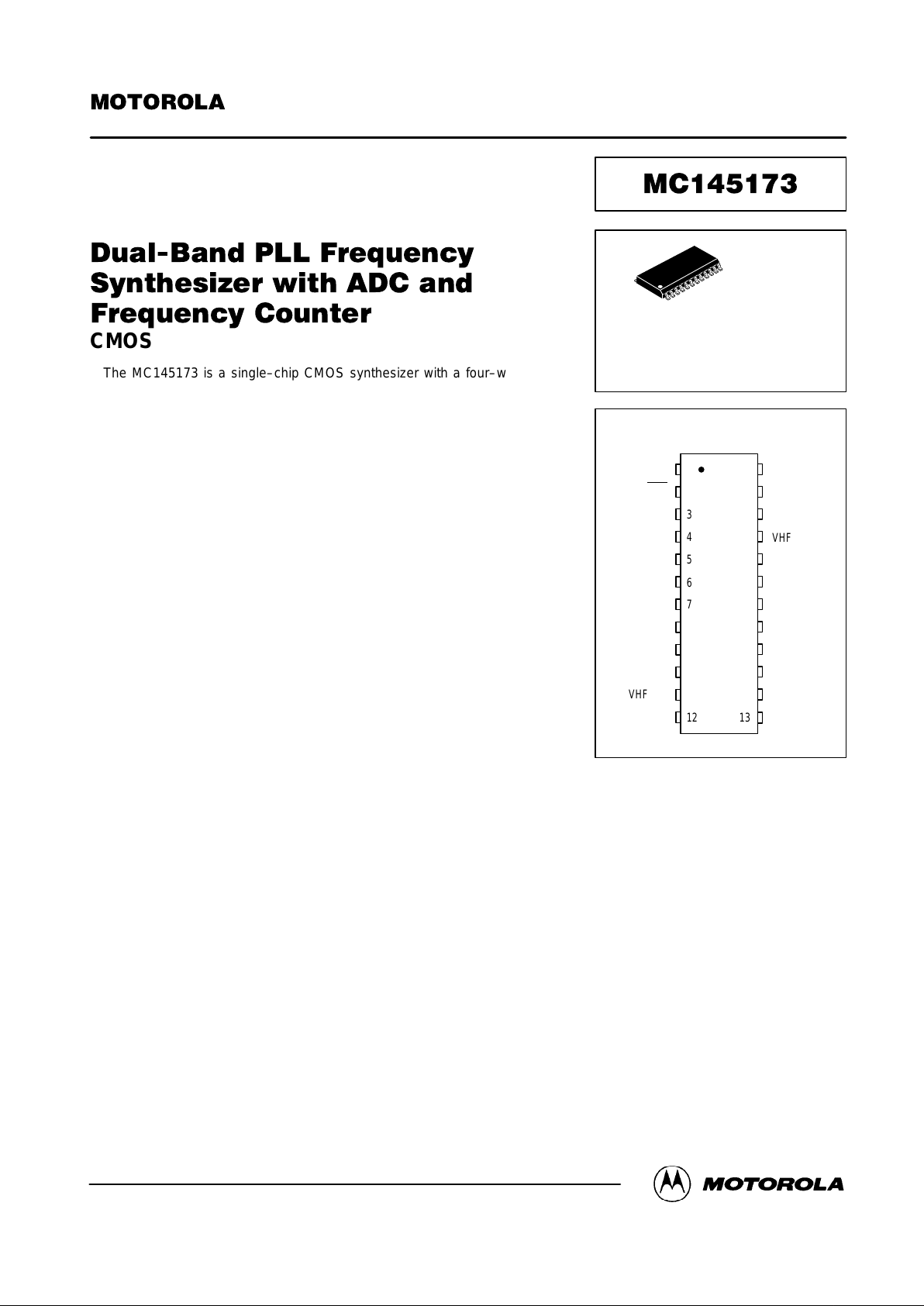
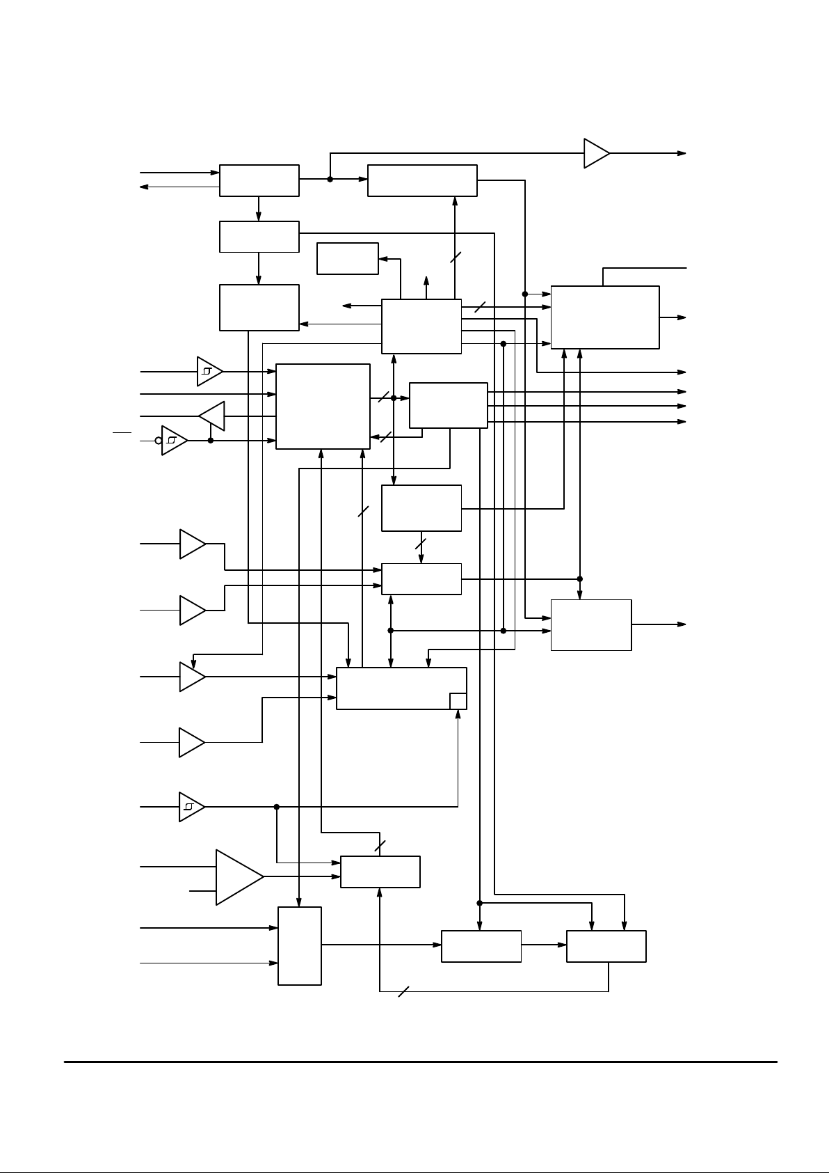
The MC145173 is a single–chip CMOS synthesizer with a four–wire serial
interface for primary use in AM–FM broadcast receivers. The device also finds
use in long–wave (LW) and short–wave (SW) receivers. Two inputs to a single
high–speed N counter are provided, along with 2 phase detectors; one for a
VHF loop up to 130 MHz, and another for an HF loop up to 40 MHz. The VHF
phase detector has a current source/sink output and both detectors feature
linear transfer functions (no dead zones). An external crystal ties across
on–chip circuitry which drives a completely–programmable reference counter.
Thus, a broad range of tuning resolution is possible. The crystal oscillator is
buffered and fed to an open–drain output which is active in the HF mode only.
Due to the patented BitGrabber registers, address or steering bits are not
needed in the serial data stream for random access of the registers. The serial
port is byte–oriented to facilitate control via an MCU. Tuning across a band is
accomplished with a two–byte transfer to the N register.
The 6–bit analog–to–digital converter (ADC) has two input channels. The
converter is read via a one–byte transfer which includes an end–of–conversion
(EOC) bit.
A 22–stage frequency counter is provided and accepts two IF (intermediate
frequency) signals. Primary use for the frequency counter is for the seek or
scan function on broadcast radio receivers. A proper frequency count ensures
tuning of valid stations on their center frequencies. Reading the count is
accomplished with a three–byte serial transfer which includes a count–complete (CC) bit.
Four general purpose digital outputs are included. One of the outputs is
open–drain; the others are totem–pole (push–pull). Two general purpose digital
inputs are provided also. One input has a comparator with a switch point at 33%
of VDD.
• Operating Voltage Range: 4.5 to 5.5 V
• Maximum Operating Frequency: VHFin= 130 MHz @ 210 mV p–p
HFin= 40 MHz @ 210 mV p–p
• Maximum Frequency of Reference Counter: 15 MHz
• Maximum Frequency of Frequency Counter: 20 MHz
• Maximum Supply Current: Operating Mode = 12 mA
Standby Mode = 30 µA
• Approximate ADC Conversion Time: 360 µs
• Operating Temperature Range: –
40 to + 85°C
• R Counter Division Range: 1 and 5 to 16,383
• N Counter Division Range: 40 to 32,767
• Accommodates Downconversion or Upconversion Receiver Design
for AM Broadcast Band
• Direct Interface to Motorola SPI Data Port
• Programmer’s Guide Included in Datasheet
BitGrabber is a trademark of Motorola, Inc.
This document contains information on a new product. Specifications and information herein are subject to change without notice.
Order this document
by MC145173/D
SEMICONDUCTOR TECHNICAL DATA
OUTPUT B
VHF
in
V
DD
HF PD
out
Rx
14
15
16
17
18
1312
VHF PD
out
OUTPUT D
OUTPUT C
V
SS
10
9
8
7
6
5
4
3
VHF IF
in
HF IF
in
INPUT A
INPUT B
INPUT D
D
out
CLK
D
in
11
20
21
22
19
PIN ASSIGNMENT
INPUT C
OUTPUT A
HF
in
DW SUFFIX
SOG PACKAGE
CASE 751E
ORDERING INFORMATION
MC145173DW SOG Package
REF
out
OSC
out
2
1
ENB
OSC
in
23
24
24
1
Motorola, Inc. 1995
REV 1
3/95
MC145173
MOTOROLA
2
BLOCK DIAGRAM
OSC
in
OSC
out
CLK
D
in
D
out
ENB
HF
in
VHF
in
HF IF
in
VHF IF
in
INPUT D
INPUT C
INPUT B
INPUT A
1
24
4
3
5
2
16
15
10
11
6
7
8
9
OSCILLATOR
STANDBY
LOGIC
SHIFT REGISTER
AND
CONTROL LOGIC
14–STAGE R COUNTER
BitGrabber
R REGISTER
24 BITS
A REGISTER
MUX
BitGrabber
N REGISTER
16 BITS
BitGrabber
C REGISTER
8 BITS
SAMPLE
AND HOLD
6–BIT ADC
22–STAGE F COUNTER
AND 24–BIT F REGISTER
CURRENT
SOURCE/SINK
PHASE/FREQUENCY
DETECTOR
PHASE/
FREQUENCY
DETECTOR
+
–
REF
out
(OPEN DRAIN)
Rx
VHF PD
out
OUTPUT D
OUTPUT C
OUTPUT B
OUTPUT A
(OPEN DRAIN)
HF PD
out
ACQUISITION
WINDOW
DIVIDER
ACQ. WINDOW
RESET
15–STAGE
N COUNTER
POL
14
2
f
R
24
ZONE
15
HF/VHF SELECT
F SMPL
RESPONSE
(INTERNALLY
CONNECTED TO VDD/3)
CONVERSION RESULT + EOC
READ
2
7
24
9
f
V
I SMPL
MUX CONTROL
23
20
21
22
14
13
12
18
PIN 17 = V
DD
PIN 19 = V
SS
PRESCALER
MC145173
3
MOTOROLA
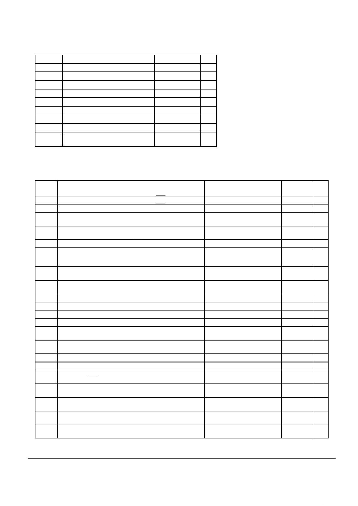
ABSOLUTE MAXIMUM RATINGS* (Voltages Referenced to V
SS
)
Symbol Parameter Value Unit
V
DD
DC Supply Voltage – 0.5 to + 6.0 V
V
in
DC Input Voltage – 0.5 to VDD + 0.5 V
V
out
DC Output Voltage – 0.5 to VDD + 0.5 V
I
in
DC Input Current, per Pin ± 10 mA
I
out
DC Output Current, per Pin ± 20 mA
I
DD
DC Supply Current, VDD and VSS Pins ± 30 mA
P
D
Power Dissipation, per Package 300 mW
T
stg
Storage Temperature – 65 to + 150 °C
T
L
Lead Temperature, 1 mm from Case
for 10 seconds
260 °C
*Maximum Ratings are those values beyond which damage to the device may occur. Func-
tional operation should be restricted to the limits in the Electrical Characteristics tables or
Pin Descriptions section.
DC ELECTRICAL CHARACTERISTICS (V
DD
= 4.5 to 5.5 V , Voltages Referenced to VSS, TA = –40 to +85°C)
Symbol
Parameter Test Condition
Guaranteed
Limit
Unit
V
IL
Maximum Low–Level Input Voltage (Din, CLK, ENB) 0.25 x V
DD
V
V
IH
Minimum High–Level Input Voltage (Din, CLK, ENB) 0.65 x V
DD
V
V
IL
Maximum Low–Level Input Voltage
(Input D, HF IFin, VHF IFin, HFin, VHFin, OSCin)
dc coupled 0.3 x V
DD
V
V
IH
Minimum High–Level Input Voltage
(Input D, HF IFin, VHF IFin, HFin, VHFin, OSCin)
dc coupled 0.7 x V
DD
V
V
Hys
Minimum Hysteresis Voltage (CLK, ENB) 0.3 V
V
TH
Threshold Voltage (INPUT C) Vin Ramped Down from V
DD
0.28 x V
DD
to
0.38 x V
DD
V
V
OL
Maximum Low–Level Output Voltage
(D
out
, OUTPUT A, OUTPUT B, OUTPUT C, OUTPUT D, HF PD
out
)
I
out
= 20 µA 0.1 V
V
OH
Minimum High–Level Output Voltage
(D
out
, OUTPUT B, OUTPUT C, OUTPUT D, HF PD
out
, REF
out
)
I
out
= –20 µA VDD – 0.1 V
I
OL
Minimum Low–Level Output Current (HF PD
out
) V
out
= 0.4 V 0.36 mA
I
OH
Minimum High–Level Output Current (HF PD
out
) V
out
= VDD – 0.4 V – 0.36 mA
I
OL
Minimum Low–Level Output Current (D
out
) V
out
= 0.4 V 1.6 mA
I
OH
Minimum High–Level Output Current (D
out
) V
out
= VDD – 0.4 V – 1.6 mA
I
OL
Minimum Low–Level Output Current
(OUTPUT B, OUTPUT C, OUTPUT D)
V
out
= 1.0 V 2.0 mA
I
OH
Minimum High–Level Output Current
(OUTPUT B, OUTPUT C, OUTPUT D)
V
out
= VDD – 1.0 V – 2.0 mA
I
OL
Minimum Low–Level Output Current (OUTPUT A) V
out
= 1.0 V 2.0 mA
I
OH
Minimum High–Level Output Current (REF
out
) V
out
= VDD – 1.0 V – 1.75 mA
I
in
Maximum Input Leakage Current
(Din, CLK, ENB, OSCin, INPUT A, INPUT B, INPUT C, INPUT D)
Vin = VDD or VSS,
Device NOT in Standby**
± 1.0 µA
I
in
Maximum Input Current
(HFin, VHFin, HF IFin, VHF IFin)
Vin = VDD or VSS,
Device NOT in Standby
± 120 µA
I
OZ
Maximum Output Leakage Current (HF PD
out
) V
out
= VDD or VSS,
Output in High–Impedance State
± 200 nA
I
OZ
Maximum Output Leakage Current (VHF PD
out
) V
out
= 1.75 or VDD – 1.5 V,
Output in High–Impedance State
± 200 nA
I
OZ
Maximum Output Leakage Current (REF
out
, OUTPUT A, D
out
) V
out
= VDD or VSS,
Output in High–Impedance State
± 2 µA
Continued on next page.
** While in Standby, the OSCin pin is pulled low by a weak on–chip FET.
This device contains protection circuitry to
guard against damage due to high static voltages or electric fields. However, precautions
must be taken to avoid applications of any voltage higher than maximum rated voltages to
this high–impedance circuit. For proper operation, Vin and V
out
should be constrained to the
range VSS ≤ (Vin or V
out
) ≤ VDD.
For proper termination of unused pins, see
the Pin Descriptions section.
MC145173
MOTOROLA
4
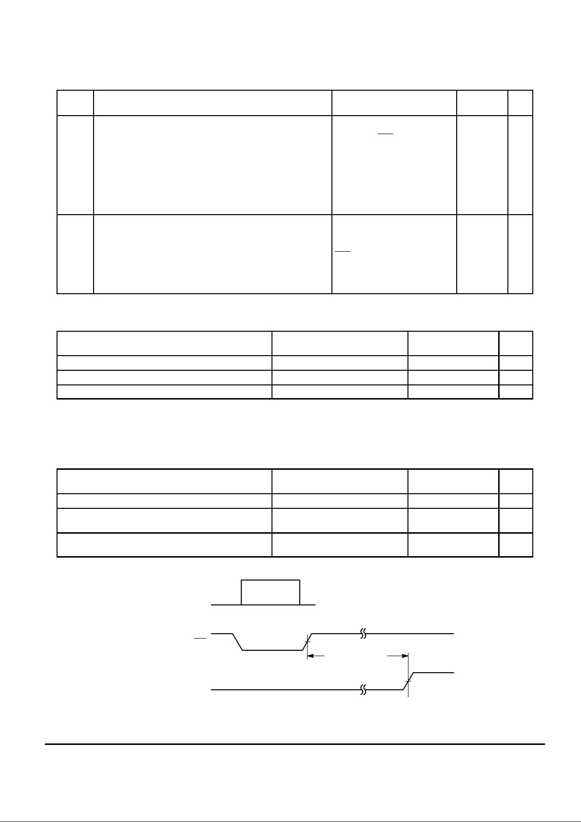
DC ELECTRICAL CHARACTERISTICS (continued) (V
DD
= 4.5 to 5.5 V , Voltages Referenced to VSS, TA = –40 to +85°C)
Symbol
Parameter Test Condition
Guaranteed
Limit
Unit
I
STBY
Maximum Standby Supply Current Vin on Din, CLK, INPUT A, INPUT
B, INPUT C, INPUT D = VDD or
VSS; Vin on ENB
= VDD; Vin on
OSCin, HF IFin, VHF IFin = VSS or
Floating (ac coupled); Vin on HF
in
= VDD or VSS or Floating (ac
coupled); Vin on VHFin = Floating
(ac coupled); D
out
tied to VDD or
VSS through 100 kΩ resistor; Other Outputs Open
30 µA
I
dd
Maximum Operating Supply Current Vin on Din, CLK, INPUT A, INPUT
B, INPUT C, INPUT D = VDD or
VSS; D
out
tied to VDD or V
SS
through 100 kΩ resistor; Vin on
ENB
= VDD; OSCin = 10.35 MHz
@ 1 V p–p; VHFin = 120 MHz @
210 mV p–p; VHF IFin = 10.7 MHz
@ 210 mV p–p
12 mA
ANALOG CHARACTERISTICS — CURRENT SOURCE/SINK OUTPUT — VHF PD
out
(I
out
≤ 2.5 mA, VDD = 4.5 to 5.5 V , Voltages Referenced to VSS)
Parameter
Test Condition
Guaranteed
Limit Unit
Maximum Source Current Variation (Part–to–Part) V
out
= 0.5 x V
DD
± 20 %
Maximum Sink–vs–Source Mismatch (Note 3) V
out
= 0.5 x V
DD
12 %
Output Voltage Range (Note 3) I
out
variation ≤ 20% 1.25 to VDD – 1.25 V V
NOTES:
1. Percentages calculated using the following formula: (Maximum Value – Minimum Value)/Maximum Value.
2. See Rx Pin Description for external resistor value.
3. This parameter is guaranteed for any specific temperature within – 40 to +
85°C.
ADC CHARACTERISTICS (T
A
= – 40 to 85°C, VDD = 4.5 to 5.5 V , f
OSC
= 9.5 to 10.4 MHz)
Parameter
Test Condition
Guaranteed
Limit Unit
Resolution 6 Bits
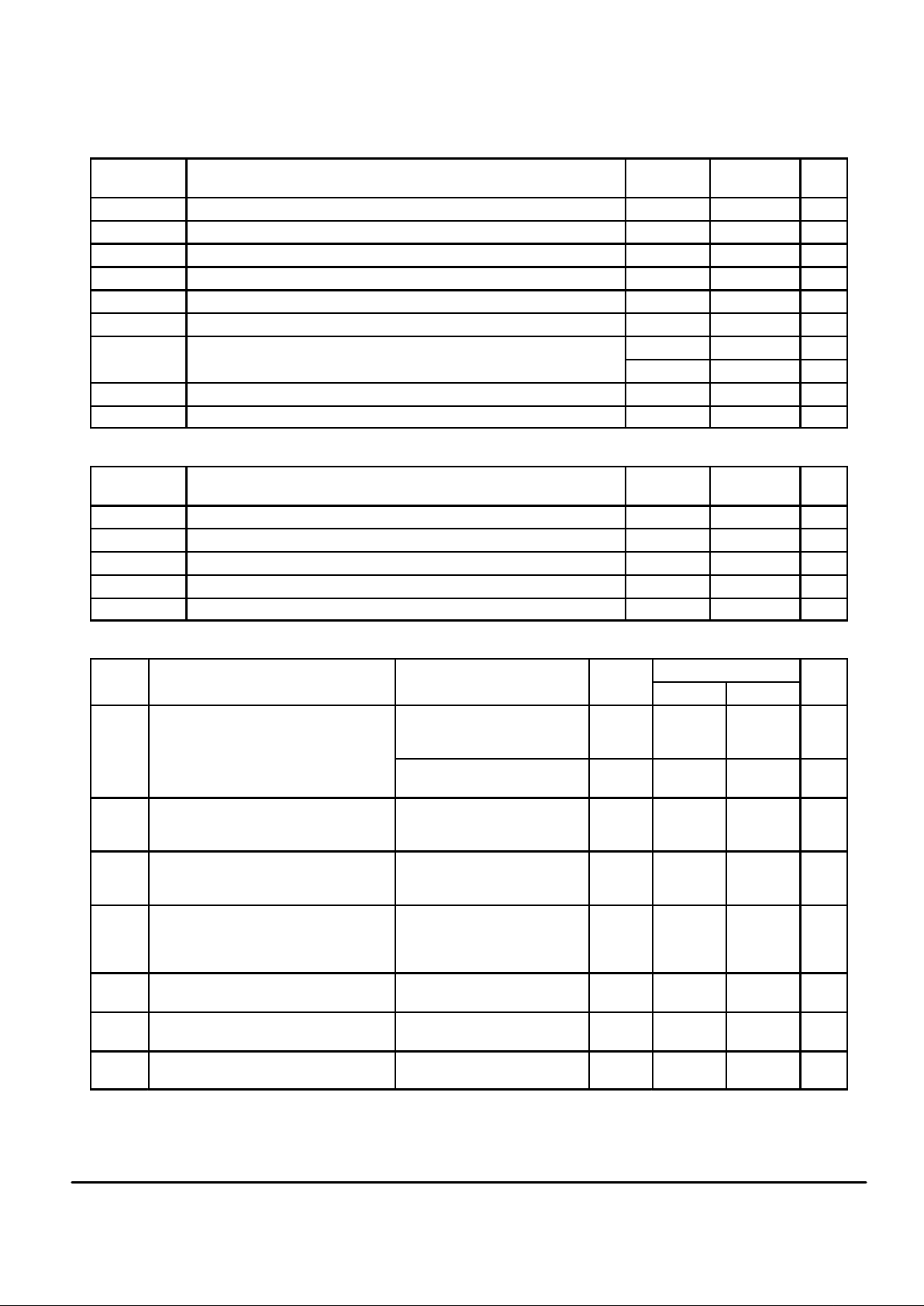
Conversion Time Per Figure 1 3584 OSC
in
Cycles
Maximum Nonlinearity Vin = VSS + (0.1 x VDD) to
VDD – (0.09 x VDD)
± 1.5 LSBs
EOC FLIP–FLOP OUTPUT
(INTERNAL)
ENB
D
in
CONVERSION TIME
SET BIT C7 HIGH
IN C REGISTER
ADC READY TO BE
READ VIA SERIAL PORT
Figure 1.
MC145173
5
MOTOROLA
AC INTERFACE CHARACTERISTICS
(VDD = 4.5 to 5.5 V , TA = – 40 to +85°C, CL = 50 pF, Input tr = tf = 10 ns unless otherwise indicated)
Symbol Parameter Figure #
Guaranteed
Limit
Unit
f
clk
Serial Data Clock Frequency (Note: Refer to CLK tw below) 2 dc to 2.1 MHz
t
PLH
, t
PHL
Maximum Propagation Delay, CLK to D
out
2, 8 150 ns
t
PLH
, t
PHL
Maximum Propagation Delay, ENB to Output B, Output C, Output D 6, 8 300 ns
t
PLZ
, t
PZL
Maximum Propagation Delay, ENB to Output A 7, 9 300 ns
t
PLZ
, t
PHZ
Maximum Disable Time, D
out
Active to High Impedance 3, 9 400 ns
t
PZL
, t
PZH
Access Time, D
out
High Impedance to Active 3, 9 0 to 200 ns
t
TLH
, t
THL
Maximum Output Transition Time, D
out
CL = 50 pF 2, 8 100 ns
CL = 200 pF 2, 8 400 ns
C
in
Maximum Input Capacitance – Din, ENB, CLK 10 pF
C
out
Maximum Output Capacitance – D
out
10 pF
TIMING REQUIREMENTS (T
A
= – 40 to + 85°C, Input tr = tf = 10 ns unless otherwise indicated)
Symbol
Parameter Figure #
Guaranteed
Limit Unit
tsu, t
h
Minimum Setup and Hold Times, Din vs CLK 4 100 ns
tsu, th, t
rec
Minimum Setup, Hold, and Recovery Times, ENB vs CLK 5 200 ns
t
w(H)
Minimum Inactive–High Pulse Width, ENB 5 600 ns
t
w
Minimum Pulse Width, CLK 2 238 ns
tr, t
f
Maximum Input Rise and Fall Times, CLK (Source Impedance ≤ 5 kΩ) 2 50 µs
AC ELECTRICAL CHARACTERISTICS (V
DD
= 4.5 to 5.5 V , TA = –40 to +85°C)
Guaranteed Range
Symbol Parameter Test Condition Figure # Min Max Unit
f
in
Input Frequency, HF
in
Vin ≥ 210 mV p–p Sine Wave,
N Counter set to divide ratio
such that fV ≤ 1 MHz (Note 1)
10 10
(Note 4)
40 MHz
Vin ≥ 2.2 V p–p Sine Wave,
N Counter same as above
10 1 40 MHz
f
in
Input Frequency, VHF
in
Vin ≥ 210 mV p–p Sine Wave,
N Counter set to divide ratio
such that fV ≤ 1 MHz (Note 1)
11 40
(Note 4)
130 MHz
f
in
Input Frequency, OSC
in
Externally driven with ac–coupled signal
(Note 2)
Vin ≥ 1.0 V p–p Sine Wave,
R Counter set to divide ratio
such that fR ≤ 1 MHz (Note 3)
12 2
(Note 4)
15 MHz
f
XTAL
Crystal Frequency, OSCin and OSC
out
(Note 2)
C1 ≤ 30 pF, C2 ≤ 30 pF,
Includes Stray Capacitance,
R Counter set to divide ratio
such that fR ≤ 1 MHz (Note 3)
13 2 15 MHz
f
in
Input Frequency, HF IF
in
Vin ≥ 85 mV p–p Sine Wave,
K bit cleared low or set high
10 400 500 kHz
f
in
Input Frequency, VHF IF
in
Vin ≥ 85 mV p–p Sine Wave 10 8
(Note 4)
20 MHz
f
out
Output Frequency, REF
out
CL = 20 pF,
V
out
≥ 1.5 V p–p
14, 15 dc 10.4 MHz
NOTES:
1. fV is the output signal of the N Counter.
2. The ADC is guaranteed over an OSCin range of 9.5 to 10.4 MHz only.
3. fR is the output signal of the R Counter.
4. For operation below this frequency, use dc coupling with a signal level of at least VIL to VIH. See Pin Description.
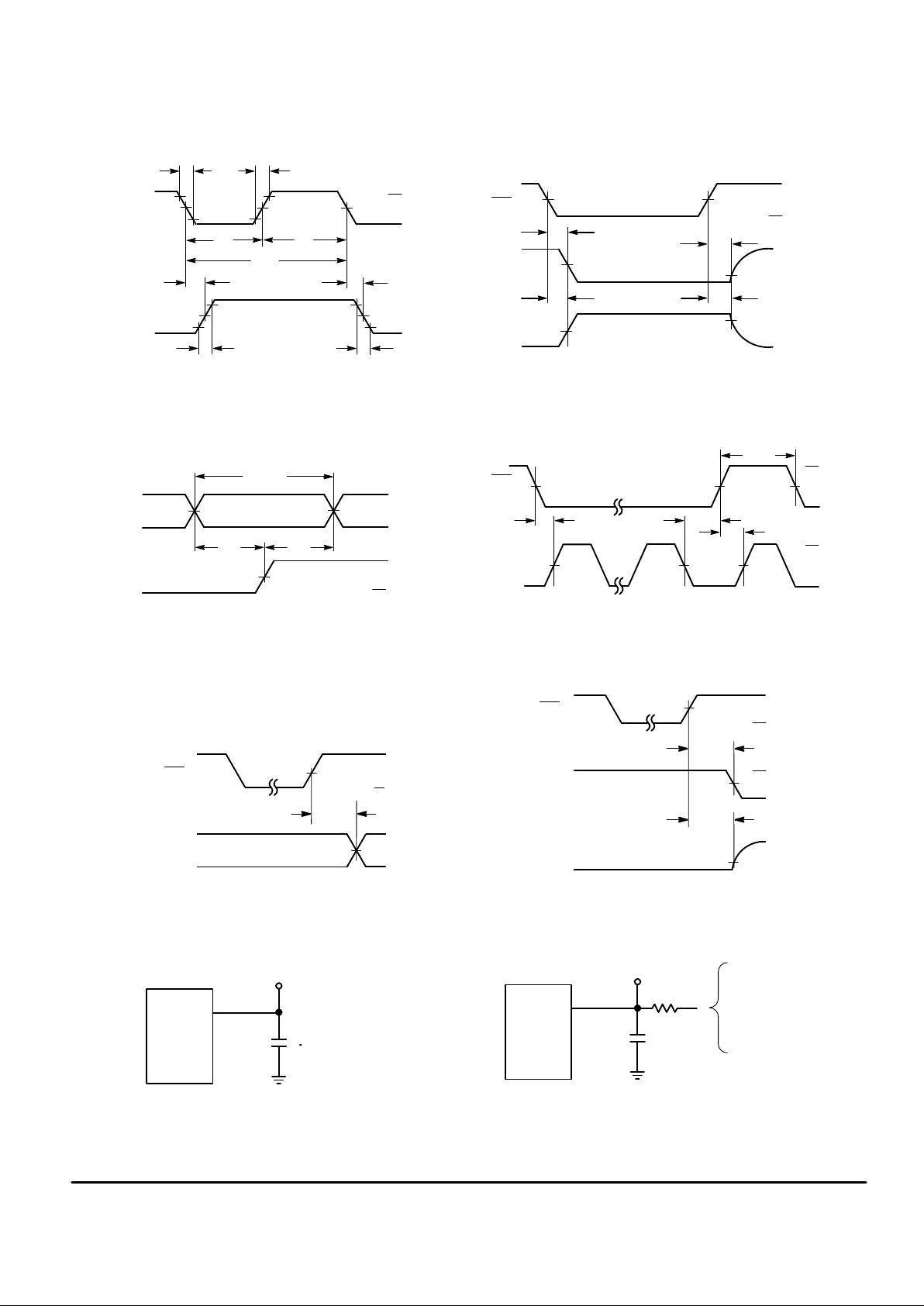
MC145173
MOTOROLA
6
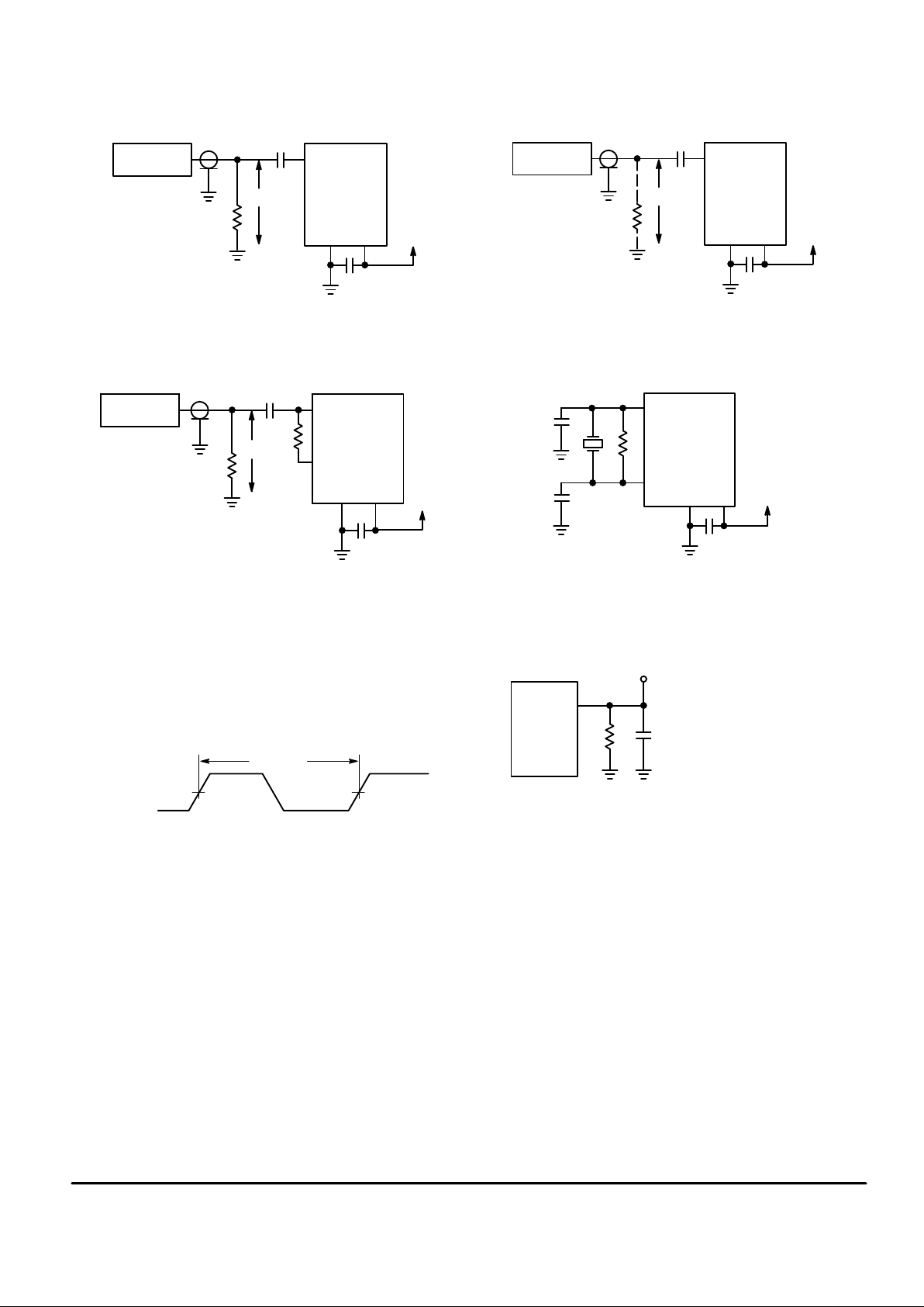
SWITCHING W AVEFORMS
10%
V
DD
V
SS
1/f
clk
D
out
CLK
90%
50%
90%
50%
10%
t
PLH
t
PHL
t
TLH
t
THL
t
w
t
w
t
f
t
r
Figure 2.
ENB
D
out
D
out
50%
V
DD
V
SS
50%
t
PZH
t
PZL
t
PLZ
50%
t
PHZ
Figure 3.
10%
90%
HIGH
IMPEDANCE
HIGH
IMPEDANCE
D
in
CLK
50%
VALID
50%
t
su
t
h
V
DD
V
SS
V
DD
V
SS
Figure 4.
CLK
ENB
50%
t
su
t
h
FIRST
CLK
LAST
CLK
t
rec
50%
Figure 5.
V
DD
V
SS
V
DD
V
SS
t
w(H)
Figure 6.
ENB
OUTPUT B,
OUTPUT C,
OUTPUT D
t
PLH
, t
PHL
50%
V
DD
V
SS
50%
Figure 7.
ENB
OUTPUT A
t
PZL
50%
V
DD
V
SS
50%
10%
OUTPUT A
t
PLZ
HIGH
IMPEDANCE
HIGH
IMPEDANCE
TEST POINT
DEVICE
UNDER
TEST
C
L
*
*Includes all probe and fixture capacitance.
Figure 8. Test Circuit
TEST POINT
DEVICE
UNDER
TEST
C
L
*
*Includes all probe and fixture capacitance.
Figure 9. Test Circuit
5 k
Ω
CONNECT TO V
DD
WHEN TESTING t
PLZ
AND t
PZL
.
CONNECT TO V
SS
WHEN TESTING t
PHZ
AND t
PZH
.
MC145173
7
MOTOROLA
SINE WAVE
GENERAT OR
MC145173
V+
V
DD
INPUT
V
in
50
Ω
Figure 10. Test Circuit
V
SS
0.01
µ
F
SINE WAVE
GENERAT OR
MC145173
V+
V
DD
VHF
in
V
in
50
Ω
*
Figure 11. Test Circuit
V
SS
* Characteristic impedance
0.01
µ
F
SINE WAVE
GENERAT OR
50
Ω
0.01 µF
V
DD
OSC
in
V
in
Figure 12. Test Circuit
V+
V
SS
MC145173
OSC
out
10 M
Ω
C1
V
DD
V
SS
OSC
in
OSC
out
C2
Figure 13. Test Circuit
V+
MC145173
50%
REF
out
1/f REF
out
Figure 14. Switching Waveform
TEST POINT
DEVICE
UNDER
TEST
C
L
*
*Includes all probe and
fixture capacitance.
Figure 15. Test Circuit
OUTPUT
1 k
Ω

MC145173
MOTOROLA
8
PIN DESCRIPTIONS
DIGITAL INTERFACE PINS
D
in
Serial Data Input (Pin 3)
The bit stream begins with the most significant bit (MSB)
and is shifted in on the low–to–high transition of CLK. The bit
pattern is 1 byte (8 bits) long to access the C register, 2 bytes
(16 bits) to access the N register, or 3 bytes (24 bits) to access the R register. (See Table 1.) The values in the C, N,
and R registers do not change during shifting because the
transfer of data to the registers is controlled by ENB
.
The bit stream needs neither address nor steering bits due
to the innovative BitGrabber registers. Therefore, all bits in
the stream are available to be data for the three registers.
Random access of any register is provided (i.e., the registers
may be accessed in any sequence). Data is retained in the
registers over a supply range of 4.5 to 5.5 V . The formats are
shown in Figures 17, 18, and 20.
Din typically switches near 45% of VDD for good noise immunity. This input can be directly interfaced to CMOS devices with outputs guaranteed to switch near rail–to–rail.
When interfacing to NMOS or TTL devices, either a level
shifter (MC74HC14A, MC14504B) or pull–up resistor of 1 to
10 kΩ must be used. Parameters to consider when sizing the
resistor are worst–case IOL of the driving device, maximum
tolerable power consumption, and maximum data rate.
Table 1Write–Only Registers
(MSBs are shifted in first, C0, N0, and R0 are the LSBs)
Number
of Clocks
Accessed
Register
Bit
Nomenclature
8
16
24
Other Values ≤ 32
Values > 32
C Register
N Register
R Register
Not Allowed
Not Allowed
C7, C6, C5, . . ., C0
N15, N14, N13, . . ., N0
R23, R22, R21, . . ., R0
Table 2Read–Only Registers
(MSBs are shifted out first; A7 and F23 are the MSBs)
Number
of Clocks
Register
Bit
Nomenclature
8, 9, or 16 A Register A7, A6, A5, . . ., A0, A#
24 F Register F23, F22, F21, . . ., F0
CLK
Serial Data Clock Input (Pin 4)
Low–to–high transitions on Clock shift bits available at Din,
while high–to–low transitions shift bits from D
out
. The chip’s
24–1/2–stage shift register is static, allowing clock rates
down to dc in a continuous or intermittent mode.
Eight clock cycles are required to access the C register.
Sixteen clock cycles are needed for the N register. 24 cycles
are used to access the R register. (See Table 1 and Figures
17, 18, and 20.)
The A register is read using 8, 9, or 16 clock cycles. The F
register is read using 24 clocks. (See Table 2 and Figures 21
and 22.)
CLK typically switches near 45% of VDD an d has a
Schmitt–triggered input buffer . See the last paragraph of D
in
for more information.
NOTE
To guarantee proper operation of the power–on
reset (POR) circuit, the CLK pin must be held at
the potential of either the VSS or VDD pin during
power up. That is, the CLK input should not be
floated or toggled while the VDD pin is ramping
from 0 to at least 4.5 V . If control of the CLK pin is
not practical during power up, then the RST bit in
the R Register must be utilized. See the R Register Bits section.
ENB
Active–Low Enable Input (Pin 2)
This pin is used to activate the serial interface to allow the
transfer of data to/from the device. When ENB
is in an inac-
tive high state, shifting is inhibited, D
out
is forced to the high–
impedance state, and the port is held in the initialized state.
To transfer data to and from the device, ENB
(which must
start inactive high) is taken low, a serial transfer is made via
Din, D
out
, and CLK, and ENB
is taken back high. The low–to–
high transition on ENB transfers data to the C, N, or R write–
only registers depending on the data stream length per
Table 1.
To minimize standby current, ENB
must be high.
CAUTION
Transitions on ENB
must not be attempted while
CLK is high. This puts the device out of synchronization with the microcontroller. Resynchronization occurs when ENB
is high and CLK is low.
This input is also Schmitt–triggered and switches near
45% of VDD, thereby minimizing the chance of loading erroneous data into the registers. See the last paragraph of D
in
for more information.
D
out
Three–State Serial Data Output (Pin 5)
Data is transferred out of the 24–1/2 stage shift register
through D
out
on the high–to–low transition of CLK. The bit
stream begins with the MSB. The bit pattern is 1 byte, 9 bits,
or 2 bytes long to read the A register. The F register’s data is
contained in 3 bytes. (See Table 2.)
Before the A register can be read, the Read A bit must be
set in the C register. Likewise, the Read F bit must be set to
read the F register.
To minimize supply current during the standby state, the
D
out
pin should not be floated. A pull–down resistor to VSS or
pull–up resistor to VDD should be used. The value can be
50 kΩ to 100 kΩ.
GENERAL–PURPOSE DIGITAL I/O PINS
Input C
Digital Input (Pin 7)
Input C is a general–purpose digital input which may be
used for MCU port expansion. The state of this input is indicated by the In C bit in the A register. (See Figure 21.)

MC145173
9
MOTOROLA
The switch point is precisely controlled by use of a
comparator. The reference for the comparator is internally
set to approximately 33% of VDD. The input has a small
amount of hysteresis voltage (approximately 50 mV).
If not used, this pin should be tied to VDD or VSS.
Input D
Digital Input (Pin 6)
Input D is a general–purpose digital input which may be
used for MCU port expansion. The state of this input is indicated by the In D bit in both the A and F registers. That is, the
state of the pin may be read from either register. (See Figures 21 and 22.)
This pin is a standard CMOS input with a switch point at
approximately 50% of VDD. Input D has a hysteresis voltage
of approximately 600 mV.
If not used, this pin should be tied to VDD or VSS.
Output A
Open–Drain Digital Output (Pin 12)
Output A is a general–purpose digital output which may be
used for MCU port expansion. An N–channel MOSFET tied
to VSS is used to drive this open–drain output. Thus, an external pull–up device is required at this pin. The state of this
output is determined by the Out A bit in the C register. (See
Figure 17.)
Upon power–up, this pin is low. If not used, Output A
should be tied to VSS or floated.
Output B
Digital Output (Pin 13)
Output B is a general–purpose digital output which may be
used for MCU port expansion. This is a standard totem–pole
(push–pull) CMOS output. The state of this output is determined by the Out B bit in the C register. (See Figure 17.)
Upon power–up, this pin is low. If not used, Output B
should be floated.
Output C
Digital Output (Pin 14)
Output C is a general–purpose digital output which may be
used for MCU port expansion. This is a standard totem–pole
(push–pull) CMOS output. The state of this output is determined by the Out C bit in the C register. (See Figure 17.)
Upon power–up, this pin is low. If not used, Output C
should be floated.
Output D
Digital Output (Pin 22)
Output D is a general–purpose digital output which may be
used for MCU port expansion. This is a standard totem–pole
(push–pull) CMOS output. The state of this output is determined by the Out D bit in the R register. (See Figure 18.)
Upon power–up, this pin is low. If not used, Output D
should be floated.
ADC INPUT PINS
Input A, Input B
Analog Inputs (Pins 9, 8)
These are inputs to the 2–channel multiplexer which feeds
the 6–bit analog–to–digital converter (ADC). The selected
channel is determined by the Chan bit in the C register.
Each pin is a high–impedance input which appears as
a mostly–capacitive load of approximately 6 pF.
If not used, these pins should be tied to VSS or VDD.
REFERENCE PINS
OSCin/OSC
out
Reference Oscillator Input/Output (Pins 1, 24)
These pins form a reference oscillator when connected to
terminals of an external parallel–resonant crystal. Frequency–setting capacitors of appropriate values as recommended by the crystal supplier are connected from each pin
to ground (up to a maximum of 30 pF each, including stray
capacitance). An external feedback resistor of 1 to 10 MΩ is
connected directly across the pins to ensure linear operation
of the amplifier. The MC145173 is designed to operate with
crystals from 2 to 15 MHz. However, frequencies are restricted to 9.5 to 10.4 MHz when the ADC is utilized. (See
Figure 13.)
If desired, an external clock source can be ac coupled to
OSCin. A 0.01 µF coupling capacitor is used for measurement purposes and is the minimum size recommended for
applications. The input capacitance of the OSCin pin is
approximately 6 pF. An external feedback resistor of approximately 10 MΩ is required across the OSCin and OSC
out
pins
in the ac–coupled case. (See Figure 12.)
OSC
out
is an internal node on the device and should not be used to drive any
loads
(i.e., OSC
out
is unbuffered). However, the buffered
REF
out
is available to drive external loads in the HF mode.
The external signal level must be at least 1 V p–p; the minimum and maximum frequencies are given in the AC Electri-
cal Characteristics table. These frequencies apply for R
Counter divide ratios as indicated in the table. For very small
ratios, the maximum frequency is limited to the divide ratio
times 1 MHz (Reason: the phase/frequency detectors are
limited to a maximum input frequency of 1 MHz).
If an external source is available which swings from at
least the VIL to VIH levels listed in the DC Electrical Charac-
teristics table, then dc coupling can be used. In the dc–
coupled case, no external feedback resistor is needed.
OSC
out
must be a No Connect to avoid loading an internal
node on the MC145173, as noted above. For frequencies below 2 MHz, a signal level of at least VIL and VIH is needed,
and dc coupling must be used. The R counter is a static
counter and may be operated down to dc. However, wave
shaping by a CMOS buffer may be required to ensure fast
rise and fall times into the OSCin pin at these low frequencies.
Each rising edge on the OSCin pin causes the R counter to
decrement by one. In the standby mode, OSCin is pulled low
by an on–chip FET.
REF
out
Open–Drain Reference Frequency Output (Pin 23)
This output is the buffered output of the crystal–generated
reference frequency or externally provided reference source.

MC145173
MOTOROLA
10
A P–channel MOSFET tied to VDD is used to drive this open–
drain output. Thus, an external pull–down device is required
at this pin. This output is disabled and assumes the high–impedance state in the VHF mode per bit HF/VHF in the R register. (See Figure 18.)
REF
out
is capable of operation to 10.4 MHz; see the AC
Electrical Characteristics table.
If unused, the pin may be floated or tied to VDD.
FREQUENCY COUNTER INPUT PINS
HF IF
in
HF Intermediate–Frequency Input (Pin 10)
This pin feeds an on–chip amplifier. The amp drives the F counter
when the HF/VHF bit in the R register is low. (See Figure 18.) The
signal driving this pin is normally sourced from the IF (intermediate
frequency) circuit in the radio and is ac coupled. The input capacitance is approximately 6 pF.
This input is optimized for use with frequencies around
450 kHz. An on–chip low–pass filter is employed to roll off response above 1 MHz. In addition, for further suppression of high–
frequency signals, the Kuligowski Acceptor Circuit may be
engaged via the K bit in the R register. This is a digital integrator
which allows acceptance of frequencies only below the frequency at
the OSCin pin divided by 8.
In the standby mode, HF IFin is pulled low by an on–chip
FET. If not used, this pin should be tied to VSS.
VHF IF
in
VHF Intermediate–Frequency Input (Pin 11)
This pin feeds an on–chip amplifier. The amp drives the F
counter when the HF/VHF bit in the R register is high. (See
Figure 18.) The signal driving this pin is normally sourced
from the IF circuit in the radio and is ac coupled. The input
capacitance is approximately 6 pF. Usually, the frequency of
the signal driving this pin is about 10.7 MHz.
For signals which swing from at least the VIL to VIH levels
listed in the DC Electrical Characteristics table, dc coupling may be used. Also, for signals less than the minimum
frequencies in the AC Electrical Characteristics table, dc
coupling with at least VIL and VIH levels is a requirement. The
F counter is a static counter and may be operated down to
dc. However, wave shaping by a CMOS buffer may be required to ensure fast rise and fall times into the VHF IFin pin.
In the standby mode, VHF IFin is forced to a high–impedence state. If not used, this pin should be tied to VSS.
LOOP PINS
HFin, VHF
in
High Frequency Input,
Very High Frequency Input (Pins 16, 15)
These pins feed on–chip amplifiers which drive the N
counter; the HF/VHF bit in the R register determines which
input is selected. (See Figure 18.) These signals are normally sourced from external voltage–controlled oscillators
(VCOs), and are ac–coupled. (See Figures 10 and 11.) The
input capacitance is approximately 6 pF. For small divide ratios, the maximum frequency is limited to the divide ratio
times 1 MHz. (Reason: the phase/frequency detectors are
limited to a maximum frequency of 1 MHz.)
For signals which swing from at least the VIL to VIH levels
listed in the DC Electrical Characteristics table, dc coupling may be used. Also, for signals less than the minimum
frequencies in the AC Electrical Characteristics table, dc
coupling with at least VIL and VIH levels is a requirement. The
N counter is a static counter and may be operated down to
dc. However, wave shaping by a CMOS buffer may be required to ensure fast rise and fall times into the HFin and
VHFin pins.
Each rising edge on these pins cause the N counter to
decrement by one.
In the standby mode, HFin is forced to a high–impedence
state, and VHFin is pulled low by an on–chip FET . If not used,
these pins should be tied to VSS.
HF PD
out
Single–Ended Phase/Frequency Detector Output
(Pin 18)
This is a three–state output for use as a loop error signal
when combined with an external low–pass filter. Through use
of a Motorola patented technique, the detector’s dead zone
has been eliminated. Therefore, the phase/frequency detector is characterized by a linear transfer function. The operation of the phase/frequency detector is described below and
is shown in Figure 16.
POL bit (R23) in the R register = low (see Figure 18)
Frequency of fV > fR or Phase of fV Leading fR: negative
pulses from high impedance
Frequency of fV < fR or Phase of fV Lagging fR: positive
pulses from high impedance
Frequency and Phase of fV = fR: essentially high–imped-
ance state; voltage at pin determined by loop filter
POL bit (R23) = high
Frequency of fV > fR or Phase of fV Leading fR: positive
pulses from high impedance
Frequency of fV < fR or Phase of fV Lagging fR: negative
pulses from high impedance
Frequency and Phase of fV = fR: essentially high–imped-
ance state; voltage at pin determined by loop filter
This output is enabled and disabled via the HF/VHF bit in
the R register. HF PD
out
is forced to the high–impedance
state when disabled. This pin should be floated when it is not
used.
VHF PD
out
Single–Ended Phase/Frequency Detector Output
(Pin 21)
This is a three–state current–source/sink output for use as
a loop error signal when combined with an external low–pass
filter. The phase/frequency detector is characterized by a linear transfer function. The operation of the phase/frequency
detector is described below and is shown in Figure 16.
POL bit (R23) in the R register = low (see Figure 18)
Frequency of fV > fR or Phase of fV Leading fR: current–
sinking pulses from a floating state
Frequency of fV < fR or Phase of fV Lagging fR: current–
sourcing pulses from a floating state
Frequency and Phase of fV = fR: essentially a floating
state; voltage at pin determined by loop filter
POL bit (R23) = high
Frequency of fV > fR or Phase of fV Leading fR: current–
sourcing pulses from a floating state
Frequency of fV < fR or Phase of fV Lagging fR: current–
sinking pulses from a floating state
 Loading...