

MOTOROLA MC14516BCP, MC14516BD, MC14516BDR2, MC14516BF, MC14516BFEL Datasheet
...
Semiconductor Components Industries, LLC, 2000
March, 2000 – Rev. 3
1 Publication Order Number:
MC14516B/D
MC14516B
Binary Up/Down Counter
The MC14516B synchronous up/down binary counter is
constructed with MOS P–channel and N–channel enhancement mode
devices in a monolithic structure.
This counter can be preset by applying the desired value, in binary,
to the Preset inputs (P0, P1, P2, P3) and then bringing the Preset
Enable (PE) high. The direction of counting is controlled by applying
a high (for up counting) or a low (for down counting) to the
UP/DOWN input. The state of the counter changes on the positive
transition of the clock input.
Cascading can be accomplished by connecting the Carry Out
to the
Carry In of the next stage while clocking each counter in parallel. The
outputs (Q0, Q1, Q2, Q3) can be reset to a low state by applying a high
to the reset (R) pin.
This CMOS counter finds primary use in up/down and difference
counting. Other applications include: (1) Frequency synthesizer
applications where low power dissipation and/or high noise immunity
is desired, (2) Analog–to–digital and digital–to–analog conversions,
and (3) Magnitude and sign generation.
• Diode Protection on All Inputs
• Supply Voltage Range = 3.0 Vdc to 18 Vdc
• Internally Synchronous for High Speed
• Logic Edge–Clocked Design — Count Occurs on Positive Going
Edge of Clock
• Single Pin Reset
• Asynchronous Preset Enable Operation
• Capable of Driving Two Low–Power TTL Loads or One Low–Power
Schottky Load Over the Rated Temperature Range
MAXIMUM RATINGS (Voltages Referenced to V
SS
) (Note 2.)
Symbol Parameter Value Unit
V
DD
DC Supply Voltage Range –0.5 to +18.0 V
Vin, V
out
Input or Output Voltage Range
(DC or Transient)
–0.5 to VDD + 0.5 V
Iin, I
out
Input or Output Current
(DC or Transient) per Pin
±10 mA
P
D
Power Dissipation,
per Package (Note 3.)
500 mW
T
A
Ambient Temperature Range –55 to +125 °C
T
stg
Storage Temperature Range –65 to +150 °C
T
L
Lead Temperature
(8–Second Soldering)
260 °C
2. Maximum Ratings are those values beyond which damage to the device
may occur.
3. Temperature Derating:
Plastic “P and D/DW” Packages: – 7.0 mW/_C From 65_C T o 125_C
http://onsemi.com
A = Assembly Location
WL or L = Wafer Lot
YY or Y = Year
WW or W = Work Week
Device Package Shipping
ORDERING INFORMATION
MC14516BCP PDIP–16 2000/Box
MC14516BD SOIC–16 48/Rail
MC14516BDR2 SOIC–16 2500/Tape & Reel
1. For ordering information on the EIAJ version of
the SOIC packages, please contact your local
ON Semiconductor representative.
MARKING
DIAGRAMS
1
16
PDIP–16
P SUFFIX
CASE 648
MC14516BCP
AWLYYWW
SOIC–16
D SUFFIX
CASE 751B
1
16
14516B
AWLYWW
SOEIAJ–16
F SUFFIX
CASE 966
1
16
MC14516B
AWLYWW
MC14516BF SOEIAJ–16 See Note 1.
MC14516BFEL SOEIAJ–16 See Note 1.
This device contains protection circuitry to guard
against damage due to high static voltages or electric
fields. However, precautions must be taken to avoid applications of any voltage higher than maximum rated
voltages to this high–impedance circuit. For proper
operation, V
in
and V
out
should be constrained to the
range V
SS
v (Vin or V
out
) v VDD.
Unused inputs must always be tied to an appropriate
logic voltage level (e.g., either V
SS
or VDD). Unused out-
puts must be left open.
MC14516B
http://onsemi.com
2
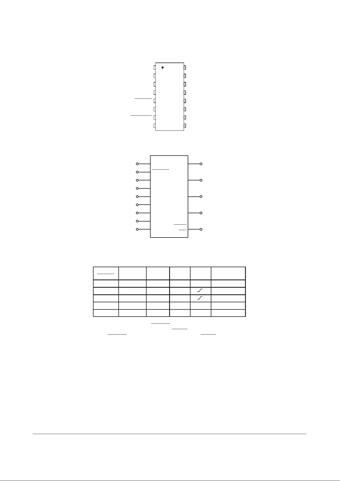
PIN ASSIGNMENT
13
14
15
16
9
10
11
125
4
3
2
1
8
7
6
P1
P2
Q2
C
V
DD
R
U/D
Q1
P0
P3
Q3
PE
V
SS
CARRY OUT
Q0
CARRY IN
BLOCK DIAGRAM
VDD = PIN 16
VSS = PIN 8
6
11
14
2
7
Q0
Q1
Q2
Q3
CARRY
OUT
PE
CARRY IN
RESET
UP/DOWN
CLOCK
P0
P1
P2
P3
1
5
9
10
15
4
12
13
3
TRUTH TABLE
Carry In Up/Down
Preset
Enable
Reset Clock Action
1 X 0 0 X No Count
0 1 0 0 Count Up
0 0 0 0 Count Down
X X 1 0 X Preset
X X X 1 X Reset
X = Don’t Care
NOTE: When counting up, the Carry Out
signal is normally high and is low only
when Q0 through Q3 are high and Carry In
is low. When counting down,
Carry Out
is low only when Q0 through Q3 and Carry In are low.
MC14516B
http://onsemi.com
3
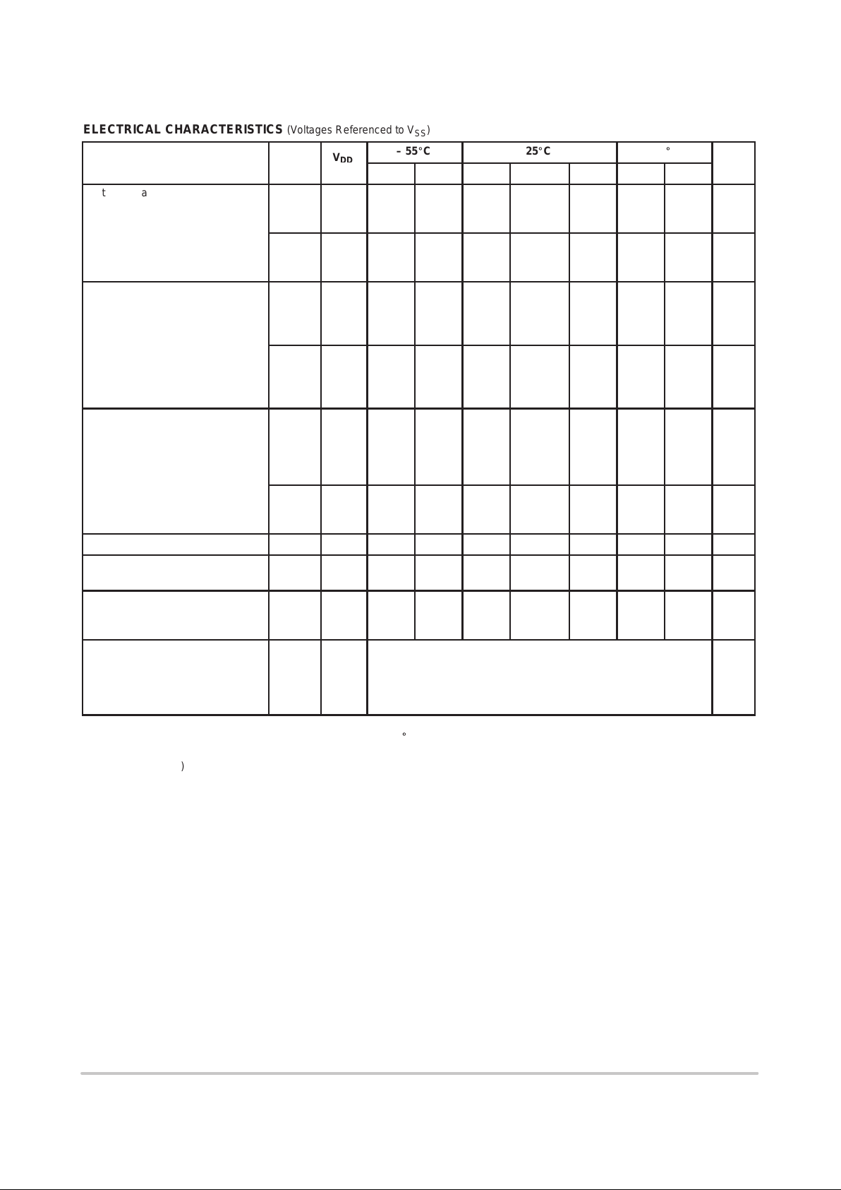
ELECTRICAL CHARACTERISTICS (Voltages Referenced to V
SS
)
V
– 55_C 25_C 125_C
Characteristic Symbol
V
DD
Vdc
Min Max Min Typ
(4.)
Max Min Max
Unit
Output Voltage “0” Level
V
in
= VDD or 0
V
OL
5.0
10
15
—
—
—
0.05
0.05
0.05
—
—
—
0
0
0
0.05
0.05
0.05
—
—
—
0.05
0.05
0.05
Vdc
“1” Level
V
in
= 0 or V
DD
V
OH
5.0
10
15
4.95
9.95
14.95
—
—
—
4.95
9.95
14.95
5.0
10
15
—
—
—
4.95
9.95
14.95
—
—
—
Vdc
Input Voltage “0” Level
(V
O
= 4.5 or 0.5 Vdc)
(V
O
= 9.0 or 1.0 Vdc)
(V
O
= 13.5 or 1.5 Vdc)
V
IL
5.0
10
15
—
—
—
1.5
3.0
4.0
—
—
—
2.25
4.50
6.75
1.5
3.0
4.0
—
—
—
1.5
3.0
4.0
Vdc
“1” Level
(V
O
= 0.5 or 4.5 Vdc)
(V
O
= 1.0 or 9.0 Vdc)
(V
O
= 1.5 or 13.5 Vdc)
V
IH
5.0
10
15
3.5
7.0
11
—
—
—
3.5
7.0
11
2.75
5.50
8.25
—
—
—
3.5
7.0
11
—
—
—
Vdc
Output Drive Current
(V
OH
= 2.5 Vdc) Source
(V
OH
= 4.6 Vdc)
(V
OH
= 9.5 Vdc)
(V
OH
= 13.5 Vdc)
I
OH
5.0
5.0
10
15
– 3.0
– 0.64
– 1.6
– 4.2
—
—
—
—
– 2.4
– 0.51
– 1.3
– 3.4
– 4.2
– 0.88
– 2.25
– 8.8
—
—
—
—
– 1.7
– 0.36
– 0.9
– 2.4
—
—
—
—
mAdc
(VOL = 0.4 Vdc) Sink
(V
OL
= 0.5 Vdc)
(V
OL
= 1.5 Vdc)
I
OL
5.0
10
15
0.64
1.6
4.2
—
—
—
0.51
1.3
3.4
0.88
2.25
8.8
—
—
—
0.36
0.9
2.4
—
—
—
mAdc
Input Current I
in
15 — ± 0.1 — ±0.00001 ± 0.1 — ± 1.0 µAdc
Input Capacitance
(V
in
= 0)
C
in
— — — — 5.0 7.5 — — pF
Quiescent Current
(Per Package)
I
DD
5.0
10
15
—
—
—
5.0
10
20
—
—
—
0.005
0.010
0.015
5.0
10
20
—
—
—
150
300
600
µAdc
Total Supply Current
(5.) (6.)
(Dynamic plus Quiescent,
Per Package)
(C
L
= 50 pF on all outputs, all
buffers switching)
I
T
5.0
10
15
IT = (0.58 µA/kHz) f + I
DD
IT = (1.20 µA/kHz) f + I
DD
IT = (1.70 µA/kHz) f + I
DD
µAdc
4. Data labelled “Typ” is not to be used for design purposes but is intended as an indication of the IC’s potential performance.
5. The formulas given are for the typical characteristics only at 25_C.
6. To calculate total supply current at loads other than 50 pF:
I
T(CL
) = IT(50 pF) + (CL – 50) Vfk
where: I
T
is in µA (per package), CL in pF, V = (VDD – VSS) in volts, f in kHz is input frequency, and k = 0.001.
MC14516B
http://onsemi.com
4
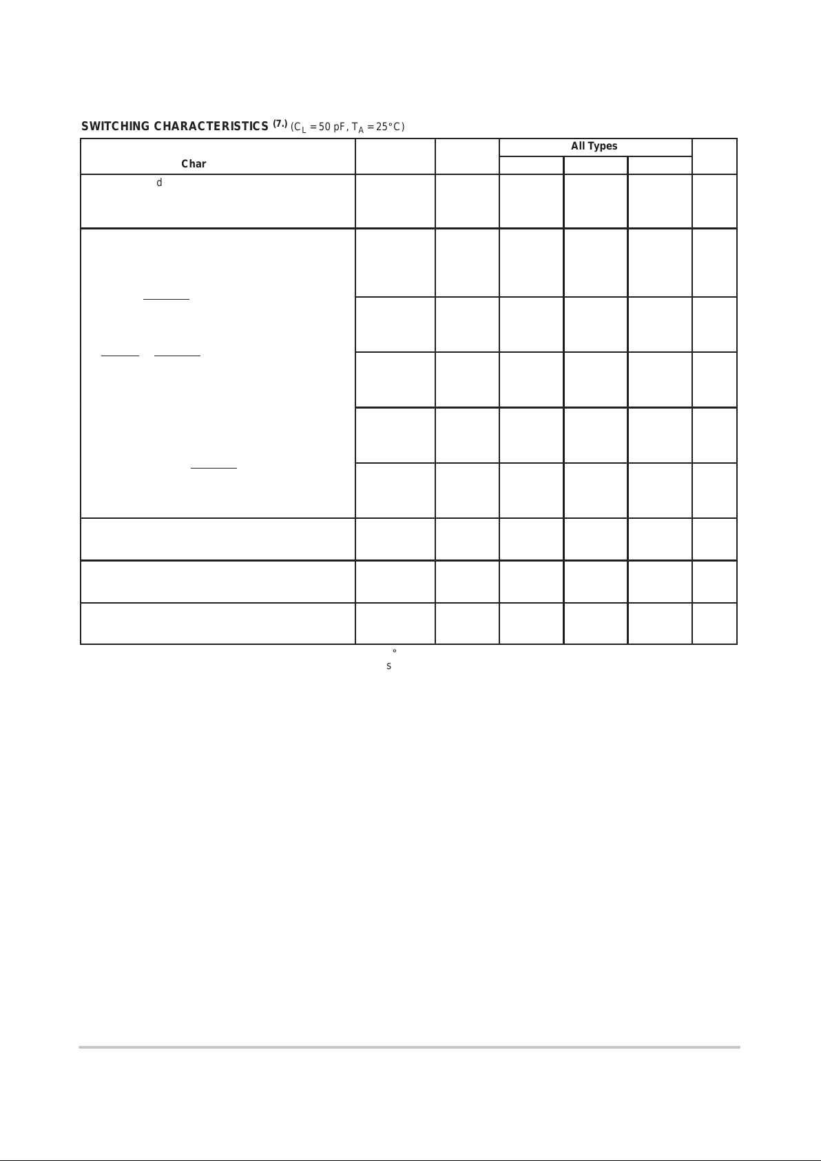
SWITCHING CHARACTERISTICS
(7.)
(C
L
= 50 pF, T
A
= 25_C)
All Types
Characteristic Symbol V
DD
Min Typ
(8.)
Max
Unit
Output Rise and Fall Time
t
TLH
, t
THL
= (1.5 ns/pF) CL + 25 ns
t
TLH
, t
THL
= (0.75 ns/pF) CL + 12.5 ns
t
TLH
, t
THL
= (0.55 ns/pF) CL + 9.5 ns
t
TLH
,
t
THL
5.0
10
15
—
—
—
100
50
40
200
100
80
ns
Propagation Delay Time
Clock to Q
t
PLH
, t
PHL
= (1.7 ns/pF) CL + 230 ns
t
PLH
, t
PHL
= (0.66 ns/pF) CL + 97 ns
t
PLH
, t
PHL
= (0.5 ns/pF) CL + 75 ns
t
PLH
,
t
PHL
5.0
10
15
—
—
—
315
130
100
630
260
200
ns
Clock to Carry Out
t
PLH
, t
PHL
= (1.7 ns/pF) CL + 230 ns
t
PLH
, t
PHL
= (0.66 ns/pF) CL + 97 ns
t
PLH
, t
PHL
= (0.5 ns/pF) CL + 75 ns
t
PLH
,
t
PHL
5.0
10
15
—
—
—
315
130
100
630
260
200
ns
Carry In to Carry Out
t
PLH
, t
PHL
= (1.7 ns/pF) CL + 230 ns
t
PLH
, t
PHL
= (0.66 ns/pF) CL + 97 ns
t
PLH
, t
PHL
= (0.5 ns/pF) CL + 75 ns
t
PLH
,
t
PHL
5.0
10
15
—
—
—
180
80
60
360
160
120
ns
Preset or Reset to Q
t
PLH
, t
PHL
= (1.7 ns/pF) CL + 230 ns
t
PLH
, t
PHL
= (0.66 ns/pF) CL + 97 ns
t
PLH
, t
PHL
= (0.5 ns/pF) CL + 75 ns
t
PLH
,
t
PHL
5.0
10
15
—
—
—
315
130
100
630
360
200
ns
Preset or Reset to Carry Out
t
PLH
, t
PHL
= (1.7 ns/pF) CL + 465 ns
t
PLH
, t
PHL
= (0.66 ns/pF) CL + 192 ns
t
PLH
, t
PHL
= (0.5 ns/pF) CL + 125 ns
t
PLH
,
t
PHL
5.0
10
15
—
—
—
550
225
150
1100
450
300
ns
Reset Pulse Width t
w
5.0
10
15
380
200
160
190
100
80
—
—
—
ns
Clock Pulse Width t
WH
5.0
10
15
350
170
140
200
100
75
—
—
—
ns
Clock Pulse Frequency f
cl
5.0
10
15
—
—
—
3.0
6.0
8.0
1.5
3.0
4.0
MHz
7. The formulas given are for the typical characteristics only at 25_C.
8. Data labelled “Typ” is not to be used for design purposes but is intended as an Indication of the IC’s potential performance.
 Loading...