

Motorola MC14516BD, MC14516BCL, MC14516BCP Datasheet
MOTOROLA CMOS LOGIC DATA
393
MC14516B
The MC14516B synchronous up/down binary counter is constructed with
MOS P–channel and N–channel enhancement mode devices in a monolithic
structure.
This counter can be preset by applying the desired value, in binary, to the
Preset inputs (P0, P1, P2, P3) and then bringing the Preset Enable (PE)
high. T he direction of counting is controlled by applying a high ( for up
counting) or a low (for down counting) to the UP/DOWN input. The state of
the counter changes on the positive transition of the clock input.
Cascading c an be accomplished by connecting the Carry Out
to the
Carry In
of the next stage while clocking e ach counter in parallel. The
outputs (Q0, Q1, Q2, Q3) can be reset to a low state by applying a high to the
reset (R) pin.
This CMOS counter finds primary use in up/down and difference counting.
Other applications include: (1) Frequency synthesizer applications where
low power dissipation and/or high noise immunity is desired, (2) Analog–to–
digital a nd digital–to–analog conversions, a nd (3) Magnitude and sign
generation.
• Diode Protection on All Inputs
• Supply Voltage Range = 3.0 Vdc to 18 Vdc
• Internally Synchronous for High Speed
• Logic Edge–Clocked Design — Count Occurs on Positive Going Edge
of Clock
• Single Pin Reset
• Asynchronous Preset Enable Operation
• Capable of Driving Two Low–Power TTL Loads or One Low–Power
Schottky Load Over the Rated Temperature Range
MAXIMUM RATINGS* (Voltages Referenced to V
SS
)
Symbol
Parameter Value Unit
V
DD
DC Supply Voltage – 0.5 to + 18.0 V
Vin, V
out
Input or Output Voltage (DC or Transient) – 0.5 to VDD + 0.5 V
Iin, I
out
Input or Output Current (DC or Transient),
per Pin
± 10 mA
P
D
Power Dissipation, per Package† 500 mW
T
stg
Storage Temperature – 65 to + 150
_
C
T
L
Lead Temperature (8–Second Soldering) 260
_
C
*Maximum Ratings are those values beyond which damage to the device may occur.
†Temperature Derating:
Plastic “P and D/DW” Packages: – 7.0 mW/_C From 65_C To 125_C
Ceramic “L” Packages: – 12 mW/_C From 100_C To 125_C
TRUTH TABLE
Carry In Up/Down
Preset
Enable
Reset Clock Action
1 X 0 0 X No Count
0 1 0 0 Count Up
0 0 0 0 Count Down
X X 1 0 X Preset
X X X 1 X Reset
X = Don’t Care
NOTE: When counting up, the Carry Out
signal is normally high and is low only
when Q0 through Q3 are high and Carry In
is low. When counting down,
Carry Out
is low only when Q0 through Q3 and Carry In are low.
SEMICONDUCTOR TECHNICAL DATA
Motorola, Inc. 1995
REV 3
1/94
L SUFFIX
CERAMIC
CASE 620
ORDERING INFORMATION
MC14XXXBCP Plastic
MC14XXXBCL Ceramic
MC14XXXBD SOIC
TA = – 55° to 125°C for all packages.
P SUFFIX
PLASTIC
CASE 648
D SUFFIX
SOIC
CASE 751B
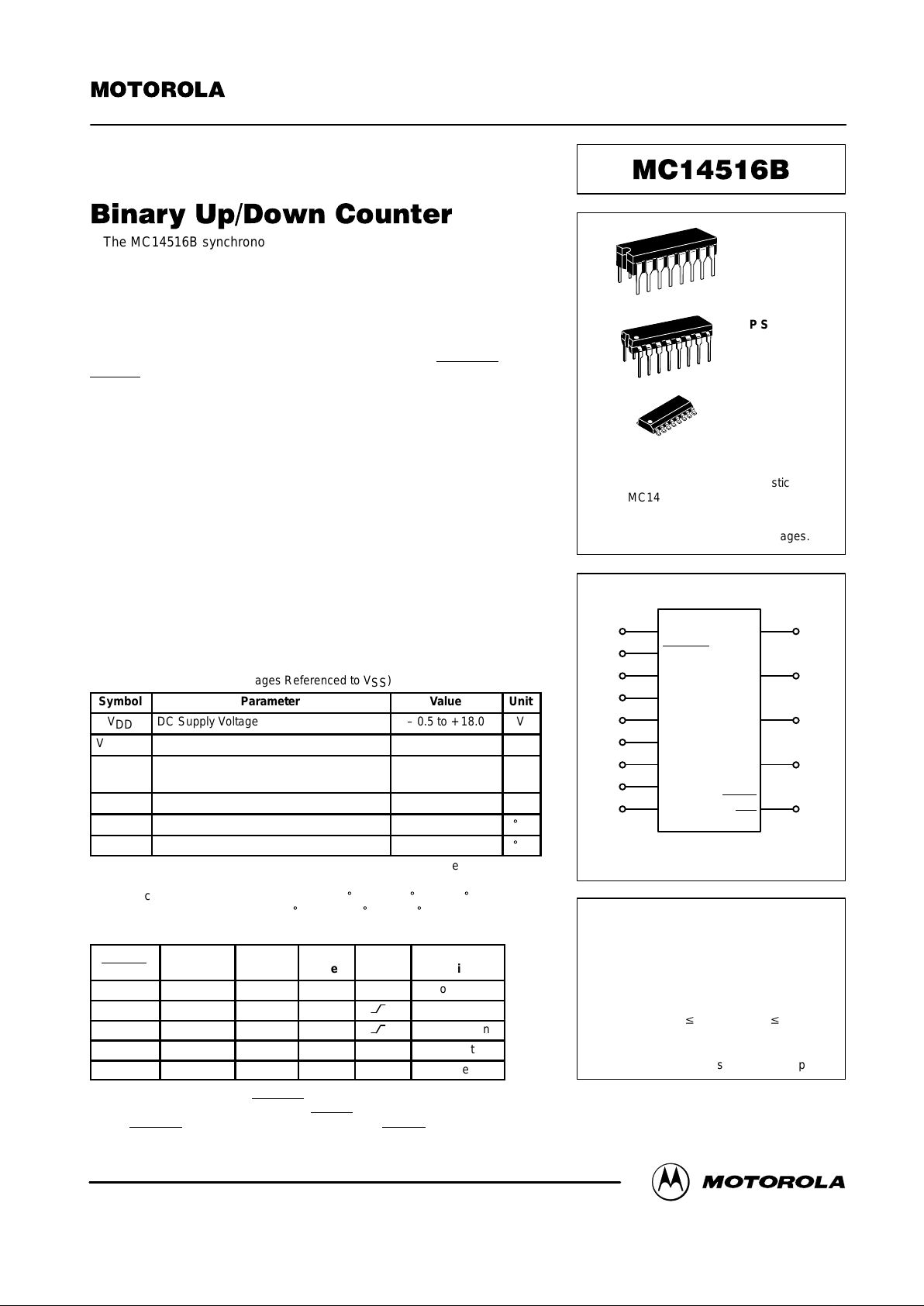
BLOCK DIAGRAM
This device contains protection circuitry to
guard against damage due to high static
voltages or electric fields. However, precautions must be taken to avoid applications of
any voltage higher than maximum rated voltages to this high–impedance circuit. For proper
operation, Vin and V
out
should be constrained
to the range VSS v (Vin or V
out
) v VDD.
Unused inputs must always be tied to an
appropriate logic voltage level (e.g., either V
SS
or VDD). Unused outputs must be left open.
VDD = PIN 16
VSS = PIN 8
6
11
14
2
7
Q0
Q1
Q2
Q3
CARRY
OUT
PE
CARRY IN
RESET
UP/DOWN
CLOCK
P0
P1
P2
P3
1
5
9
10
15
4
12
13
3
MOTOROLA CMOS LOGIC DATAMC14516B
394
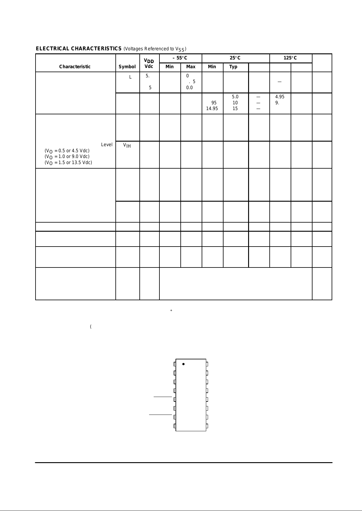
ELECTRICAL CHARACTERISTICS (Voltages Referenced to V
SS
)
V
– 55_C 25_C 125_C
Characteristic
Symbol
V
DD
Vdc
Min Max Min Typ # Max Min Max
Unit
Output Voltage
“0” Level
Vin = VDD or 0
V
OL
5.0
10
15
—
—
—
0.05
0.05
0.05
—
—
—
0
0
0
0.05
0.05
0.05
—
—
—
0.05
0.05
0.05
Vdc
“1” Level
Vin = 0 or V
DD
V
OH
5.0
10
15
4.95
9.95
14.95
—
—
—
4.95
9.95
14.95
5.0
10
15
—
—
—
4.95
9.95
14.95
—
—
—
Vdc
Input Voltage
“0” Level
(VO = 4.5 or 0.5 Vdc)
(VO = 9.0 or 1.0 Vdc)
(VO = 13.5 or 1.5 Vdc)
V
IL
5.0
10
15
—
—
—
1.5
3.0
4.0
—
—
—
2.25
4.50
6.75
1.5
3.0
4.0
—
—
—
1.5
3.0
4.0
Vdc
“1” Level
(VO = 0.5 or 4.5 Vdc)
(VO = 1.0 or 9.0 Vdc)
(VO = 1.5 or 13.5 Vdc)
V
IH
5.0
10
15
3.5
7.0
11
—
—
—
3.5
7.0
11
2.75
5.50
8.25
—
—
—
3.5
7.0
11
—
—
—
Vdc
Output Drive Current
(VOH = 2.5 Vdc) Source
(VOH = 4.6 Vdc)
(VOH = 9.5 Vdc)
(VOH = 13.5 Vdc)
I
OH
5.0
5.0
10
15
– 3.0
– 0.64
– 1.6
– 4.2
—
—
—
—
– 2.4
– 0.51
– 1.3
– 3.4
– 4.2
– 0.88
– 2.25
– 8.8
—
—
—
—
– 1.7
– 0.36
– 0.9
– 2.4
—
—
—
—
mAdc
(VOL = 0.4 Vdc) Sink
(VOL = 0.5 Vdc)
(VOL = 1.5 Vdc)
I
OL
5.0
10
15
0.64
1.6
4.2
—
—
—
0.51
1.3
3.4
0.88
2.25
8.8
—
—
—
0.36
0.9
2.4
—
—
—
mAdc
Input Current I
in
15 — ± 0.1 — ±0.00001 ± 0.1 — ± 1.0 µAdc
Input Capacitance
(Vin = 0)
C
in
— — — — 5.0 7.5 — — pF
Quiescent Current
(Per Package)
I
DD
5.0
10
15
—
—
—
5.0
10
20
—
—
—
0.005
0.010
0.015
5.0
10
20
—
—
—
150
300
600
µAdc
Total Supply Current**†
(Dynamic plus Quiescent,
Per Package)
(CL = 50 pF on all outputs, all
buffers switching)
I
T
5.0
10
15
IT = (0.58 µA/kHz) f + I
DD
IT = (1.20 µA/kHz) f + I
DD
IT = (1.70 µA/kHz) f + I
DD
µAdc
#Data labelled “Typ” is not to be used for design purposes but is intended as an indication of the IC’s potential performance.
**āThe formulas given are for the typical characteristics only at 25_C.
†To calculate total supply current at loads other than 50 pF:
IT(CL) = IT(50 pF) + (CL – 50) Vfk
where: IT is in µA (per package), CL in pF, V = (VDD – VSS) in volts, f in kHz is input frequency, and k = 0.001.
PIN ASSIGNMENT
13
14
15
16
9
10
11
125
4
3
2
1
8
7
6
P1
P2
Q2
C
V
DD
R
U/D
Q1
P0
P3
Q3
PE
V
SS
CARRY OUT
Q0
CARRY IN
MOTOROLA CMOS LOGIC DATA
395
MC14516B
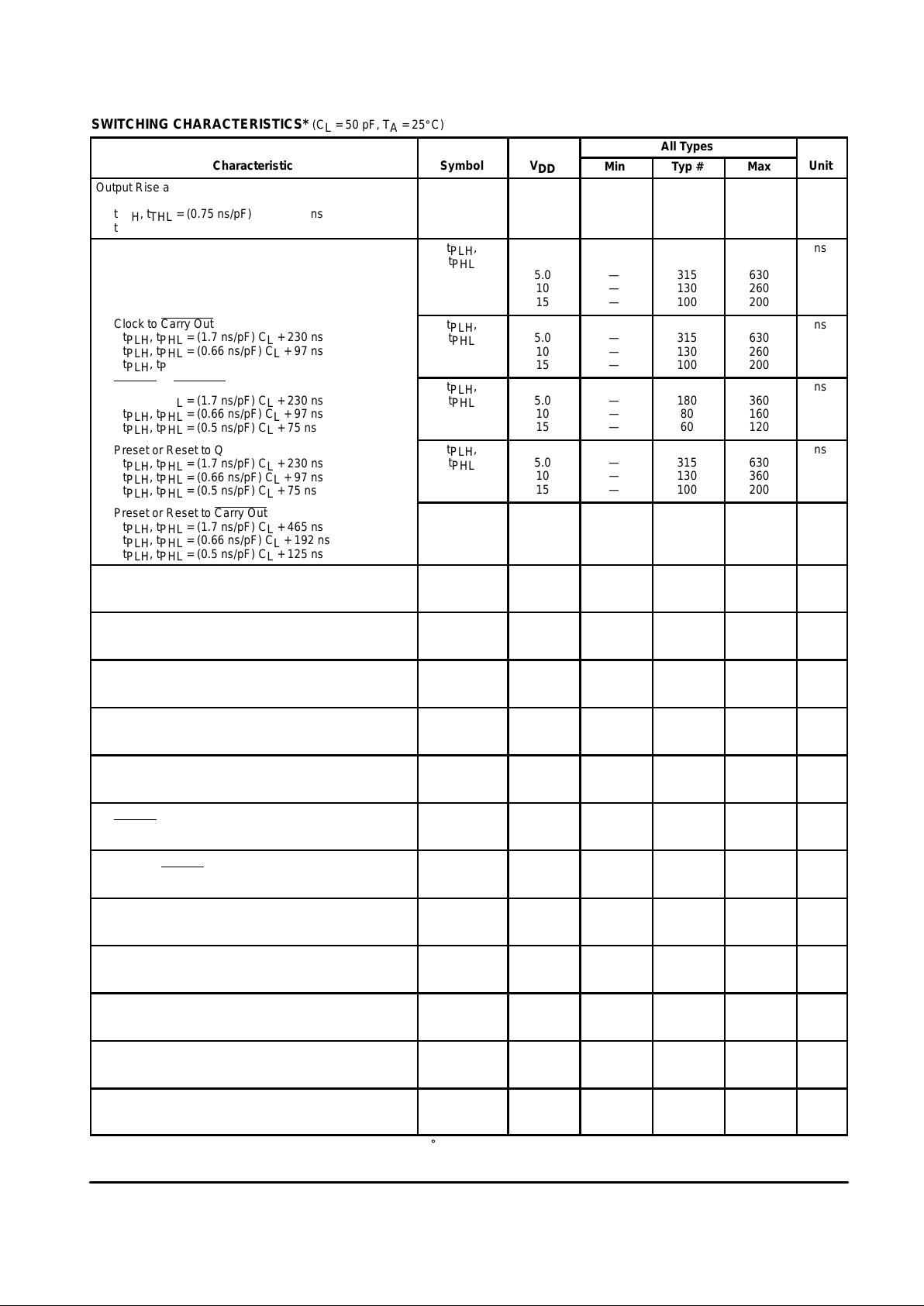
SWITCHING CHARACTERISTICS* (C
L
= 50 pF, TA = 25_C)
All Types
Characteristic
Symbol
V
DD
Min Typ # Max
Unit
Output Rise and Fall Time
t
TLH
, t
THL
= (1.5 ns/pF) CL + 25 ns
t
TLH
, t
THL
= (0.75 ns/pF) CL + 12.5 ns
t
TLH
, t
THL
= (0.55 ns/pF) CL + 9.5 ns
t
TLH
,
t
THL
5.0
10
15
—
—
—
100
50
40
200
100
80
ns
Propagation Delay Time
Clock to Q
t
PLH
, t
PHL
= (1.7 ns/pF) CL + 230 ns
t
PLH
, t
PHL
= (0.66 ns/pF) CL + 97 ns
t
PLH
, t
PHL
= (0.5 ns/pF) CL + 75 ns
t
PLH
,
t
PHL
5.0
10
15
—
—
—
315
130
100
630
260
200
ns
Clock to Carry Out
t
PLH
, t
PHL
= (1.7 ns/pF) CL + 230 ns
t
PLH
, t
PHL
= (0.66 ns/pF) CL + 97 ns
t
PLH
, t
PHL
= (0.5 ns/pF) CL + 75 ns
t
PLH
,
t
PHL
5.0
10
15
—
—
—
315
130
100
630
260
200
ns
t
PLH
, t
PHL
= (1.7 ns/pF) CL + 230 ns
t
PLH
, t
PHL
= (0.66 ns/pF) CL + 97 ns
t
PLH
, t
PHL
= (0.5 ns/pF) CL + 75 ns
Carry In
to Carry Out
t
PLH
, t
PHL
= (1.7 ns/pF) CL + 230 ns
t
PLH
, t
PHL
= (0.66 ns/pF) CL + 97 ns
t
PLH
, t
PHL
= (0.5 ns/pF) CL + 75 ns
t
PLH
,
t
PHL
5.0
10
15
—
—
—
180
80
60
360
160
120
ns
t
PLH
, t
PHL
= (1.7 ns/pF) CL + 230 ns
t
PLH
, t
PHL
= (0.66 ns/pF) CL + 97 ns
t
PLH
, t
PHL
= (0.5 ns/pF) CL + 75 ns
Carry In
to Carry Out
t
PLH
, t
PHL
= (1.7 ns/pF) CL + 230 ns
t
PLH
, t
PHL
= (0.66 ns/pF) CL + 97 ns
t
PLH
, t
PHL
= (0.5 ns/pF) CL + 75 ns
Preset or Reset to Q
t
PLH
, t
PHL
= (1.7 ns/pF) CL + 230 ns
t
PLH
, t
PHL
= (0.66 ns/pF) CL + 97 ns
t
PLH
, t
PHL
= (0.5 ns/pF) CL + 75 ns
t
PLH
,
t
PHL
5.0
10
15
—
—
—
315
130
100
630
360
200
ns
t
PLH
, t
PHL
= (1.7 ns/pF) CL + 230 ns
t
PLH
, t
PHL
= (0.66 ns/pF) CL + 97 ns
t
PLH
, t
PHL
= (0.5 ns/pF) CL + 75 ns
Carry In
to Carry Out
t
PLH
, t
PHL
= (1.7 ns/pF) CL + 230 ns
t
PLH
, t
PHL
= (0.66 ns/pF) CL + 97 ns
t
PLH
, t
PHL
= (0.5 ns/pF) CL + 75 ns
Preset or Reset to Q
t
PLH
, t
PHL
= (1.7 ns/pF) CL + 230 ns
t
PLH
, t
PHL
= (0.66 ns/pF) CL + 97 ns
t
PLH
, t
PHL
= (0.5 ns/pF) CL + 75 ns
Preset or Reset to Carry Out
t
PLH
, t
PHL
= (1.7 ns/pF) CL + 465 ns
t
PLH
, t
PHL
= (0.66 ns/pF) CL + 192 ns
t
PLH
, t
PHL
= (0.5 ns/pF) CL + 125 ns
t
PLH
,
t
PHL
5.0
10
15
—
—
—
550
225
150
1100
450
300
ns
Reset Pulse Width t
w
5.0
10
15
380
200
160
190
100
80
—
—
—
ns
Clock Pulse Width t
WH
5.0
10
15
350
170
140
200
100
75
—
—
—
ns
Clock Pulse Frequency f
cl
5.0
10
15
—
—
—
3.0
6.0
8.0
1.5
3.0
4.0
MHz
Preset or Reset Removal Time
The Preset or Reset signal must be low prior to a
positive–going transition of the clock.
t
rem
5.0
10
15
650
230
180
325
115
90
—
—
ns
Clock Rise and Fall Time t
TLH
,
t
THL
5.0
10
15
—
—
—
—
—
—
15
5
4
µs
Setup Time
Carry In
to Clock
t
su
5.0
10
15
260
120
100
130
60
50
—
—
—
ns
Hold Time
Clock to Carry In
t
h
5.0
10
15
0
20
20
– 60
– 20
0
—
—
—
ns
Setup Time
Up/Down to Clock
t
su
5.0
10
15
500
200
150
250
100
75
—
—
—
ns
Hold Time
Clock to Up/Down
t
h
5.0
10
15
– 70
– 10
0
– 160
– 60
– 40
—
—
—
ns
Setup Time
Pn to PE
t
su
5.0
10
15
– 40
– 30
– 25
– 120
– 70
– 50
—
—
—
ns
Hold Time
PE to Pn
t
h
5.0
10
15
480
420
420
240
210
210
—
—
—
ns
Preset Enable Pulse Width t
WH
5.0
10
15
200
100
80
100
50
40
—
—
—
ns
*The formulas given are for the typical characteristics only at 25_C.
#Data labelled “Typ” is not to be used for design purposes but is intended as an Indication of the IC’s potential performance.
 Loading...