

MOTOROLA CMOS LOGIC DATAMC14500B
306
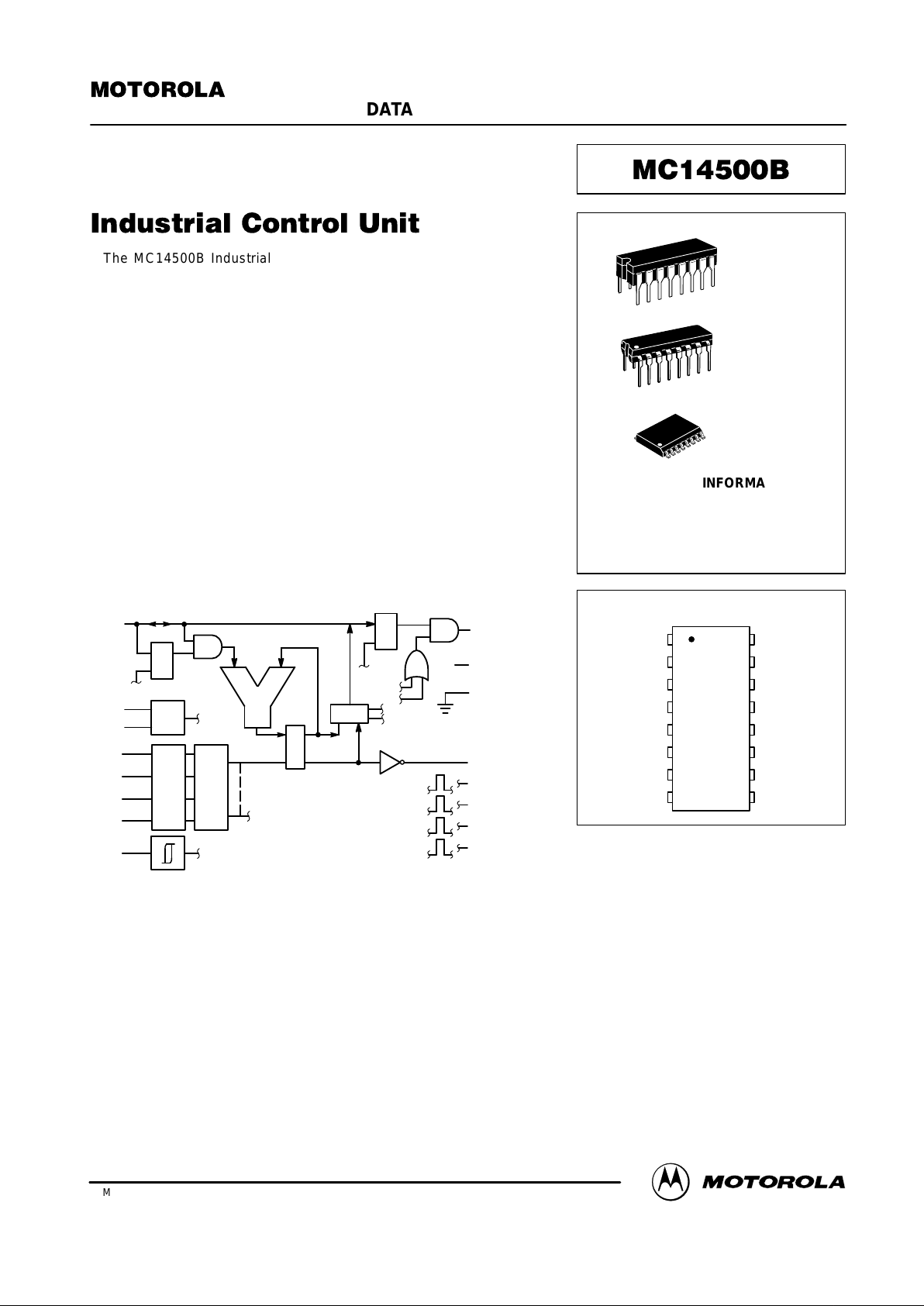
The M C14500B I ndustrial C ontrol Unit (ICU) i s a single–bit C MOS
processor. The ICU is designed for use in systems requiring decisions based
on successive single–bit information. An external ROM stores the control
program. With a program counter (and output latches and input multiplexers,
if required) the ICU in a system forms a stored–program controller that
replaces combinatorial logic. Applications include relay logic processing,
serial data manipulation and control. The ICU also may control an MPU or be
controlled by an MPU.
• 16 Instructions
• DC to 1.0 MHz Operation at VDD = 5 V
• On–Chip Clock (Oscillator)
• Executes One Instruction per Clock Cycle
• 3 to 18 V Operation
• Low Quiescent Current Characteristic of CMOS Devices
• Capable of Driving One Low–Power Schottky Load or Two Low–Power
TTL Loads over Full Temperature Range
BLOCK DIAGRAM
DATA
X1
X2
I0
I1
I2
I3
RST
3
14
13
7
6
5
4
1
INST
REG
OSC
D
C
IEN
LU
D
C
RESULT
REG. (RR)
MUX
D
C
16
2
8
WRITE
V
DD
V
SS
15
12
11
10
9
RR
JMP
RTN
FLAG O
FLAG F
+V
OEN
STOC
STO
X1 — OSCILLATOR OUTPUT
X2 — OSCILLATOR INPUT
SEMICONDUCTOR TECHNICAL DATA
Motorola, Inc. 1995
REV 3
1/94
L SUFFIX
CERAMIC
CASE 620
ORDERING INFORMATION
TA = – 55° to 125°C for all packages.
P SUFFIX
PLASTIC
CASE 648
DW SUFFIX
SOIC
CASE 751G
PIN ASSIGNMENT
MC14XXXBCP Plastic
MC14XXXBCL Ceramic
MC14XXXBDW SOIC
13
14
15
16
9
10
11
125
4
3
2
1
8
7
6
JMP
X2
X1
V
DD
FLAG F
FLAG O
RTN
I3
DATA
WRITE
RST
V
SS
I0
I1
I2
RR
MOTOROLA CMOS LOGIC DATA
307
MC14500B
MAXIMUM RATINGS* (Voltages Referenced to V
SS
)
Symbol
Parameter
Value
Unit
V
DD
DC Supply Voltage
– 0.5 to + 18.0
V
Vin, V
out
Input or Output Voltage (DC or Transient)
– 0.5 to VDD + 0.5
V
Iin,
Iout
Input or Output Current (DC or Transient),
per Pin
± 10
mA
P
D
Power Dissipation, per Package†
500
mW
T
stg
Storage Temperature
– 65 to + 150
_
C
T
L
Lead Temperature (8–Second Soldering)
260
_
C
*Maximum Ratings are those values beyond which damage to the device may occur.
†Temperature Derating:
Plastic “P and D/DW” Packages: – 7.0 mW/_C From 65_C To 125_C
Ceramic “L” Packages: – 12 mW/_C From 100_C To 125_C
ELECTRICAL CHARACTERISTICS (Voltages Referenced to V
SS
)
V
– 55_C
25_C
125_C
Characteristic
Symbol
V
DD
Vdc
Min
Max
Min
Typ #
Max
Min
ÎÎÎ
ÎÎÎ
ÎÎÎ
Max
Unit
Output Voltage
“0” Level
Vin = VDD or 0
V
OL
5.0
10
15
—
—
—
0.05
0.05
0.05
—
—
—
0
0
0
0.05
0.05
0.05
—
—
—
ÎÎÎ
ÎÎÎ
ÎÎÎ
ÎÎÎ
0.05
0.05
0.05
Vdc
“1” Level
Vin = 0 or V
DD
V
OH
5.0
10
15
4.95
9.95
14.95
—
—
—
4.95
9.95
14.95
5.0
10
15
—
—
—
4.95
9.95
14.95
ÎÎÎ
ÎÎÎ
ÎÎÎ
ÎÎÎ
—
—
—
Vdc
Input Voltage
“0” Level
RST, D, X2
(VO = 4.5 or 0.5 Vdc)
(VO = 9.0 or 1.0 Vdc)
(VO = 13.5 or 1.5 Vdc)
V
IL
5.0
10
15
—
—
—
1.5
3.0
4.0
—
—
—
2.25
4.50
6.75
1.5
3.0
4.0
—
—
—
ÎÎÎ
ÎÎÎ
ÎÎÎ
ÎÎÎ
ÎÎÎ
ÎÎÎ
1.5
3.0
4.0
Vdc
“1” Level
(VO = 0.5 or 4.5 Vdc)
(VO = 1.0 or 9.0 Vdc)
(VO = 1.5 or 13.5 Vdc)
V
IH
5.0
10
15
3.5
7.0
11
—
—
—
3.5
7.0
11
2.75
5.50
8.25
—
—
—
3.5
7.0
11
ÎÎÎ
ÎÎÎ
ÎÎÎ
ÎÎÎ
—
—
—
Vdc
Input Voltage #
“0” Level
I0, I1, I2, I3
(VO = 4.5 or 0.5 Vdc)
(VO = 9.0 or 1.0 Vdc)
(VO = 13.5 or 1.5 Vdc)
V
IL
5.0
10
15
—
—
—
0.8
1.6
2.4
—
—
—
1.1
2.2
3.4
0.8
1.6
2.4
—
—
—
ÎÎÎ
ÎÎÎ
ÎÎÎ
ÎÎÎ
ÎÎÎ
ÎÎÎ
0.8
1.6
2.4
Vdc
“1” Level
(VO = 0.5 or 4.5 Vdc)
(VO = 1.0 or 9.0 Vdc)
(VO = 1.5 or 13.5 Vdc)
V
IH
5.0
10
15
2.0
6.0
10
—
—
—
2.0
6.0
10
1.9
3.1
4.3
—
—
—
2.0
6.0
10
ÎÎÎ
ÎÎÎ
ÎÎÎ
ÎÎÎ
ÎÎÎ
—
—
—
Vdc
Output Drive Current Source
Data, Write
(VOH = 4.6 Vdc)
(VOH = 9.5 Vdc)
(VOH = 13.5 Vdc)
I
OH
5.0
10
15
– 1.2
– 3.6
– 7.2
—
—
—
– 1.0
– 3.0
– 6.0
– 2.0
– 6.0
– 12
—
—
—
– 0.7
– 2.1
– 4.2
ÎÎÎ
ÎÎÎ
ÎÎÎ
ÎÎÎ
ÎÎÎ
—
—
—
mAdc
(VOL = 0.4 Vdc) Sink
(VOL = 0.5 Vdc)
(VOL = 1.5 Vdc)
I
OL
5.0
10
15
1.9
3.6
7.2
—
—
—
1.6
3.0
6.0
3.2
6.0
12
—
—
—
1.1
2.1
4.2
ÎÎÎ
ÎÎÎ
ÎÎÎ
ÎÎÎ
ÎÎÎ
—
—
—
mAdc
Output Drive Current Source
Other Outputs
(VOH = 2.5 Vdc)
(VOH = 4.6 Vdc)
(VOH = 9.5 Vdc)
(VOH = 13.5 Vdc)
I
OH
5.0
5.0
10
15
– 3.0
– 0.64
– 1.6
– 4.2
—
—
—
—
– 2.4
– 0.51
– 1.3
– 3.4
– 4.2
– 0.88
– 2.25
– 8.8
—
—
—
—
– 1.7
– 0.36
– 0.9
– 2.4
ÎÎÎ
ÎÎÎ
ÎÎÎ
ÎÎÎ
ÎÎÎ
ÎÎÎ
—
—
—
—
mAdc
(VOL = 0.4 Vdc) Sink
(VOL = 0.5 Vdc)
(VOL = 1.5 Vdc)
I
OL
5.0
10
15
0.64
1.6
4.2
—
—
—
0.51
1.3
3.4
0.88
2.25
8.8
—
—
—
0.36
0.9
2.4
ÎÎÎ
ÎÎÎ
ÎÎÎ
ÎÎÎ
—
—
—
mAdc
#Data labelled “Typ” is not to be used for design purposes but is intended as an indication of the IC’s potential performance.
This device contains protection circuitry to
guard against damage due to high static
voltages or electric fields. However, precautions must be taken to avoid applications of
any voltage higher than maximum rated voltages to this high–impedance circuit. For proper
operation, Vin and V
out
should be constrained
to the range VSS v (Vin or V
out
) v VDD.
Unused inputs must always be tied to an
appropriate logic voltage level (e.g., either V
SS
or VDD). Unused outputs must be left open.
MOTOROLA CMOS LOGIC DATAMC14500B
308
ELECTRICAL CHARACTERISTICS — continued (Voltages Referenced to V
SS
)
V
–55_C
25_C
125_C
Characteristic
Symbol
V
DD
Vdc
Min
Max
Min
Typ #
Max
Min
ÎÎÎ
ÎÎÎ
ÎÎÎ
Max
Unit
Input Current, RST
I
in
15
25
—
—
150
—
—
ÎÎÎ
ÎÎÎ
ÎÎÎ
250
µAdc
Input Current
I
in
15
—
± 0.1
—
±0.00001
± 0.1
—
ÎÎÎ
ÎÎÎ
± 1.0
µAdc
Input Capacitance (Data)
C
in
—
—
—
—
15
—
—
ÎÎÎ
ÎÎÎ
ÎÎÎ
—
pF
Input Capacitance (All Other Inputs)
C
in
—
—
—
—
5.0
7.5
—
ÎÎÎ
ÎÎÎ
ÎÎÎ
—
pF
Quiescent Current
(Per Package) I
out
= 0 µA,
Vin = 0 or V
DD
I
DD
5.0
10
15
—
—
—
5.0
10
20
—
—
—
0.005
0.010
0.015
5.0
10
20
—
—
—
ÎÎÎ
ÎÎÎ
ÎÎÎ
ÎÎÎ
150
300
600
µAdc
**Total Supply Current at an
External Load Capacitance (CL)
on All Outputs
I
T
—
IT = (1.5 µA/kHz) f + I
DD
IT = (3.0 µA/kHz) f + I
DD
IT = (4.5 µA/kHz) f + I
DD
µAdc
**The formulas given are for the typical characteristics only at 25_C.
#Data labelled “Typ” is not to be used for design purposes but is intended as an indication of the IC’s potential performance.
SWITCHING CHARACTERISTICS* (T
A
= 25_C; tr = tf = 20 ns for X and I inputs; CL = 50 pF for JMP, X1, RR, Flag O, Flag F;
CL = 130 pF + 1 TTL load for Data and Write.)
ÎÎÎÎ
ÎÎÎÎ
ÎÎÎÎ
V
ОООООООООО
ОООООООООО
ОООООООООО
All Types
Characteristic
ÎÎÎÎ
ÎÎÎÎ
ÎÎÎÎ
Symbol
V
DD
Vdc
ÎÎÎÎ
ÎÎÎÎ
ÎÎÎÎ
Min
Typ #
Max
Unit
Propagation Delay Time, X1 to RR
ÎÎÎÎ
ÎÎÎÎ
ÎÎÎÎ
ÎÎÎÎ
t
PLH
,
t
PHL
5.0
10
15
ÎÎÎÎ
ÎÎÎÎ
ÎÎÎÎ
ÎÎÎÎ
—
—
—
250
125
100
500
250
200
ns
X1 to Flag F, Flag O, RTN, JMP
ÎÎÎÎ
ÎÎÎÎ
ÎÎÎÎ
ÎÎÎÎ
5.0
10
15
ÎÎÎÎ
ÎÎÎÎ
ÎÎÎÎ
ÎÎÎÎ
—
—
—
200
100
85
400
200
170
X1 to Write
ÎÎÎÎ
ÎÎÎÎ
ÎÎÎÎ
ÎÎÎÎ
5.0
10
15
ÎÎÎÎ
ÎÎÎÎ
ÎÎÎÎ
ÎÎÎÎ
—
—
—
225
125
100
450
250
200
X1 to Data
ÎÎÎÎ
ÎÎÎÎ
ÎÎÎÎ
ÎÎÎÎ
5.0
10
15
ÎÎÎÎ
ÎÎÎÎ
ÎÎÎÎ
ÎÎÎÎ
—
—
—
250
120
100
500
240
200
RST to RR
ÎÎÎÎ
ÎÎÎÎ
ÎÎÎÎ
ÎÎÎÎ
5.0
10
15
ÎÎÎÎ
ÎÎÎÎ
ÎÎÎÎ
ÎÎÎÎ
—
—
—
250
125
100
500
250
200
RST to X1
ÎÎÎÎ
ÎÎÎÎ
ÎÎÎÎ
ÎÎÎÎ
5.0
10
15
ÎÎÎÎ
ÎÎÎÎ
ÎÎÎÎ
ÎÎÎÎ
—
—
—
450
200
150
Note 1
RST to Flag F, Flag O, RTN, JMP
ÎÎÎÎ
ÎÎÎÎ
ÎÎÎÎ
ÎÎÎÎ
5.0
10
15
ÎÎÎÎ
ÎÎÎÎ
ÎÎÎÎ
ÎÎÎÎ
—
—
—
400
200
150
800
400
300
RST to Write, Data
ÎÎÎÎ
ÎÎÎÎ
ÎÎÎÎ
ÎÎÎÎ
5.0
10
15
ÎÎÎÎ
ÎÎÎÎ
ÎÎÎÎ
ÎÎÎÎ
—
—
—
450
225
175
900
450
350
Clock Pulse Width, X1
ÎÎÎÎ
ÎÎÎÎ
ÎÎÎÎ
ÎÎÎÎ
t
W(cl)
5.0
10
15
ÎÎÎÎ
ÎÎÎÎ
ÎÎÎÎ
ÎÎÎÎ
400
200
180
200
100
90
—
—
—
ns
Rent Pulse Width, RST
ÎÎÎÎ
ÎÎÎÎ
ÎÎÎÎ
ÎÎÎÎ
t
W(R)
5.0
10
15
ÎÎÎÎ
ÎÎÎÎ
ÎÎÎÎ
ÎÎÎÎ
500
250
200
250
125
100
—
—
—
ns
Setup Time — Instruction
ÎÎÎÎ
ÎÎÎÎ
ÎÎÎÎ
ÎÎÎÎ
t
su(l)
5.0
10
15
ÎÎÎÎ
ÎÎÎÎ
ÎÎÎÎ
ÎÎÎÎ
400
250
180
200
125
90
—
—
—
ns
Data
ÎÎÎÎ
ÎÎÎÎ
ÎÎÎÎ
ÎÎÎÎ
t
su(D)
5.0
10
15
ÎÎÎÎ
ÎÎÎÎ
ÎÎÎÎ
ÎÎÎÎ
200
100
80
100
50
40
—
—
—
Hold Time — Instruction
ÎÎÎÎ
ÎÎÎÎ
ÎÎÎÎ
ÎÎÎÎ
t
h(l)
5.0
10
15
ÎÎÎÎ
ÎÎÎÎ
ÎÎÎÎ
ÎÎÎÎ
100
50
50
0
0
0
—
—
—
ns
Data
ÎÎÎÎ
ÎÎÎÎ
ÎÎÎÎ
ÎÎÎÎ
t
h(D)
5.0
10
15
ÎÎÎÎ
ÎÎÎÎ
ÎÎÎÎ
ÎÎÎÎ
200
100
100
100
50
50
—
—
—
NOTE 1. Maximum Reset Delay may extend to one–half clock period.
#Data labelled “Typ” is not to be used for design purposes but is intended as an indication of the IC’s potential performance.

MOTOROLA CMOS LOGIC DATA
309
MC14500B
Figure 1. Typical Clock Frequency
versus Resistor (RC)
RC, CLOCK FREQUENCY RESISTOR
10 k
Ω
100 k
Ω
1 M
Ω
f
Clk
, CLOCK FREQUENCY (Hz)
100 k
1 M
10 k
ÎÎÎÎ
ÎÎÎÎ
ÎÎÎÎ
Pin No.
Function
Symbols
ÎÎÎÎ
ÎÎÎÎ
ÎÎÎÎ
ÎÎÎÎ
ÎÎÎÎ
ÎÎÎÎ
ÎÎÎÎ
ÎÎÎÎ
ÎÎÎÎ
ÎÎÎÎ
ÎÎÎÎ
ÎÎÎÎ
ÎÎÎÎ
1
2
3
4
5
6
7
8
9
10
11
12
13
14
15
16
Chip Reset
Write Pulse
Data In/Out
MSB Instruction Word
Bit 2 Instruction Word
Bit 1 Instruction Word
LSB Instruction Word
Negative Supply (Ground)
Flag on NOP F
Flag on NOP O
Subroutine Return Flag
Jump Instruction Flag
Oscillator Input
Oscillator Output
Result Register
Positive Supply
RST
Write
Data
I
3
I
2
I
1
I
0
V
SS
Flag F
Flag O
RTN
JMP
X2
X1
RR
V
DD
Table 1. MC14500B Instruction Set
Instruction Code
Mnemonic
Action
0
1
2
3
4
5
6
7
8
9
A
B
C
D
E
F
0000
0001
0010
0011
0100
0101
0110
0111
1000
1001
1010
1011
1100
1101
1110
1111
NOPO
LD
LDC
AND
ANDC
OR
ORC
XNOR
STO
STOC
IEN
OEN
JMP
RTN
SKZ
NOPF
No change in registers. RR RR, Flag O
Load result register. Data RR
Load complement. Data RR
Logical AND. RR Data RR
Logical AND complement. RR Data
RR
Logical OR. RR + Data RR
Logical OR complement. RR + Data
RR
Exclusive NOR. If RR = Data, RR 1
Store. RR Data Pin, Write
Store complement. RR
Data Pin, Write
Input enable. Data IEN Register
Output enable. Data OEN Register
Jump. JMP Flag
Return. RTN Flag and skip next instruction
Skip next instruction if RR = 0
No change in registers. RR RR, Flag F
Figure 2. Outline of a Typical Organization for a MC14500B–Based System
MEMORY
PROGRAM
COUNTER
MC14500B
ICU
CLOCK
DATA
I/O ADDRESS
I0, I1, I2, I
3
ADDITIONAL
OUTPUT DEVICES
MC14599B
8–BIT ADDRESSABLE LATCH
WITH BIDIRECTIONAL DATA
MC14512
8–CHANNEL
DATA SELECTOR
ADDITIONAL
INPUT DEVICES
8
INPUTS
8
OUTPUTS
TO PERIPHERAL
DEVICES
4 BIT OP CODE
DATA BUS
MEMORY
ADDRESS

MOTOROLA CMOS LOGIC DATAMC14500B
310
TIMING WAVEFORMS
Instructions NOPO, NOPF
Instructions RR, IEN, OEN remain unaffected
Instructions SKZ, JMP, RTN
Instructions RR, IEN, OEN remain unaffected
X1
RST
IEN
REGISTER
OEN
REGISTER
RR
4–BIT
INSTRUCTION
FLAG 0
FLAG F
t
W(R)
t
PHL
(RESET TO XI)
t
PHL
(RESET TO RR)
NOP0 NOPF NOPO
t
PLH
(DATA TO FLAG)
t
PHL
X1
4–BIT
INSTRUCTION
RST
RR
JMP FLAG
RTN FLAG
SKP F/F
INTERNAL
*Instructions Ignored.
t
W(cl)
SKZ * JMP RTN * JMP
t
PHL
(RESET TO JUMP)

MOTOROLA CMOS LOGIC DATA
311
MC14500B
TIMING WAVEFORMS
Instructions STO, STOC, OEN
Instructions LD, LDC, AND, ANDC
Instructions OR, ORC, XNOR, IEN
1
X1
4–BIT
INSTRUCTION
DATA
RR
OEN REGISTER
(INTERNAL)
WRITE
STO
STOC
STO
STOC
NOP OEN STO
STOC
t
PLH
, t
PHL
(X1 TO DATA)
t
PHL
t
PLH
VALID WHEN RST = L
NOTE 1. Valid output data.
X1
4–BIT
INSTRUCTION
DATA
RR
IEN REGISTER
(INTERNAL)
LD, etc.
t
su(D)
t
su(I)
NOP IEN LD, etc.
t
h(I)
t
h(D)
t
PLH
, t
PHL
(X1 TO RR)
VALID WHEN RST = L

MOTOROLA CMOS LOGIC DATAMC14500B
312
OUTLINE DIMENSIONS
P SUFFIX
PLASTIC DIP PACKAGE
CASE 648–08
ISSUE R
NOTES:
1. DIMENSIONING AND TOLERANCING PER ANSI
Y14.5M, 1982.
2. CONTROLLING DIMENSION: INCH.
3. DIMENSION L TO CENTER OF LEADS WHEN
FORMED PARALLEL.
4. DIMENSION B DOES NOT INCLUDE MOLD FLASH.
5. ROUNDED CORNERS OPTIONAL.
–A–
B
F
C
S
H
G
D
J
L
M
16 PL
SEATING
1 8
916
K
PLANE
–T–
M
A
M
0.25 (0.010) T
DIM MIN MAX MIN MAX
MILLIMETERSINCHES
A 0.740 0.770 18.80 19.55
B 0.250 0.270 6.35 6.85
C 0.145 0.175 3.69 4.44
D 0.015 0.021 0.39 0.53
F 0.040 0.70 1.02 1.77
G 0.100 BSC 2.54 BSC
H 0.050 BSC 1.27 BSC
J 0.008 0.015 0.21 0.38
K 0.110 0.130 2.80 3.30
L 0.295 0.305 7.50 7.74
M 0 10 0 10
S 0.020 0.040 0.51 1.01
____
L SUFFIX
CERAMIC DIP PACKAGE
CASE 620–10
ISSUE V
NOTES:
1. DIMENSIONING AND TOLERANCING PER
ANSI Y14.5M, 1982.
2. CONTROLLING DIMENSION: INCH.
3. DIMENSION L TO CENTER OF LEAD WHEN
FORMED PARALLEL.
4. DIMENSION F MAY NARROW TO 0.76 (0.030)
WHERE THE LEAD ENTERS THE CERAMIC
BODY.
–A–
–B–
–T–
F
E
G
N
K
C
SEATING
PLANE
16 PLD
S
A
M
0.25 (0.010) T
16 PLJ
S
B
M
0.25 (0.010) T
M
L
DIM MIN MAX MIN MAX
MILLIMETERSINCHES
A 0.750 0.785 19.05 19.93
B 0.240 0.295 6.10 7.49
C ––– 0.200 ––– 5.08
D 0.015 0.020 0.39 0.50
E 0.050 BSC 1.27 BSC
F 0.055 0.065 1.40 1.65
G 0.100 BSC 2.54 BSC
H 0.008 0.015 0.21 0.38
K 0.125 0.170 3.18 4.31
L 0.300 BSC 7.62 BSC
M 0 15 0 15
N 0.020 0.040 0.51 1.01
_ _ _ _
16 9
1 8

MOTOROLA CMOS LOGIC DATA
313
MC14500B
OUTLINE DIMENSIONS
DW SUFFIX
PLASTIC SOIC PACKAGE
CASE 751G–02
ISSUE A
DIM MIN MAX MIN MAX
INCHESMILLIMETERS
A 10.15 10.45 0.400 0.411
B 7.40 7.60 0.292 0.299
C 2.35 2.65 0.093 0.104
D 0.35 0.49 0.014 0.019
F 0.50 0.90 0.020 0.035
G 1.27 BSC 0.050 BSC
J 0.25 0.32 0.010 0.012
K 0.10 0.25 0.004 0.009
M 0 7 0 7
P 10.05 10.55 0.395 0.415
R 0.25 0.75 0.010 0.029
M
B
M
0.010 (0.25)
NOTES:
1. DIMENSIONING AND TOLERANCING PER ANSI
Y14.5M, 1982.
2. CONTROLLING DIMENSION: MILLIMETER.
3. DIMENSIONS A AND B DO NOT INCLUDE MOLD
PROTRUSION.
4. MAXIMUM MOLD PROTRUSION 0.15 (0.006) PER
SIDE.
5. DIMENSION D DOES NOT INCLUDE DAMBAR
PROTRUSION. ALLOWABLE DAMBAR
PROTRUSION SHALL BE 0.13 (0.005) TOTAL IN
EXCESS OF D DIMENSION AT MAXIMUM
MATERIAL CONDITION.
–A–
–B– P8X
G14X
D16X
SEATING
PLANE
–T–
S
A
M
0.010 (0.25) B
S
T
16 9
81
F
J
R
X 45
_
_ _ _ _
M
C
K
How to reach us:
USA/EUROPE/Locations Not Listed: Motorola Literature Distribution; JAPAN: Nippon Motorola Ltd.; Tatsumi–SPD–JLDC, 6F Seibu–Butsuryu–Center,
P.O. Box 20912; Phoenix, Arizona 85036. 1–800–441–2447 or 602–303–5454 3–14–2 Tatsumi Koto–Ku, Tokyo 135, Japan. 03–81–3521–8315
MFAX: RMFAX0@email.sps.mot.com – TOUCHTONE 602–244–6609 ASIA/PACIFIC: Motorola Semiconductors H.K. Ltd.; 8B Tai Ping Industrial Park,
INTERNET: http://Design–NET.com 51 Ting Kok Road, Tai Po, N.T., Hong Kong. 852–26629298
Motorola reserves the right to make changes without further notice to any products herein. Motorola makes no warranty , representation or guarantee regarding
the suitability of its products for any particular purpose, nor does Motorola assume any liability arising out of the application or use of any product or circuit,
and specifically disclaims any and all liability, including without limitation consequential or incidental damages. “Typical” parameters which may be provided
in Motorola data sheets and/or specifications can and do vary in different applications and actual performance may vary over time. All operating parameters,
including “Typicals” must be validated for each customer application by customer’s technical experts. Motorola does not convey any license under its patent
rights nor the rights of others. Motorola products are not designed, intended, or authorized for use as components in systems intended for surgical implant
into the body, or other applications intended to support or sustain life, or for any other application in which the failure of the Motorola product could create a
situation where personal injury or death may occur. Should Buyer purchase or use Motorola products for any such unintended or unauthorized application,
Buyer shall indemnify and hold Motorola and its officers, employees, subsidiaries, affiliates, and distributors harmless against all claims, costs, damages, and
expenses, and reasonable attorney fees arising out of, directly or indirectly, any claim of personal injury or death associated with such unintended or
unauthorized use, even if such claim alleges that Motorola was negligent regarding the design or manufacture of the part. Motorola and are registered
trademarks of Motorola, Inc. Motorola, Inc. is an Equal Opportunity/Affirmative Action Employer .
MC14500B/D
*MC14500B/D*
◊
 Loading...