

SEMICONDUCTOR
TECHNICAL DATA
PERIPHERAL
DRIVER ARRAYS
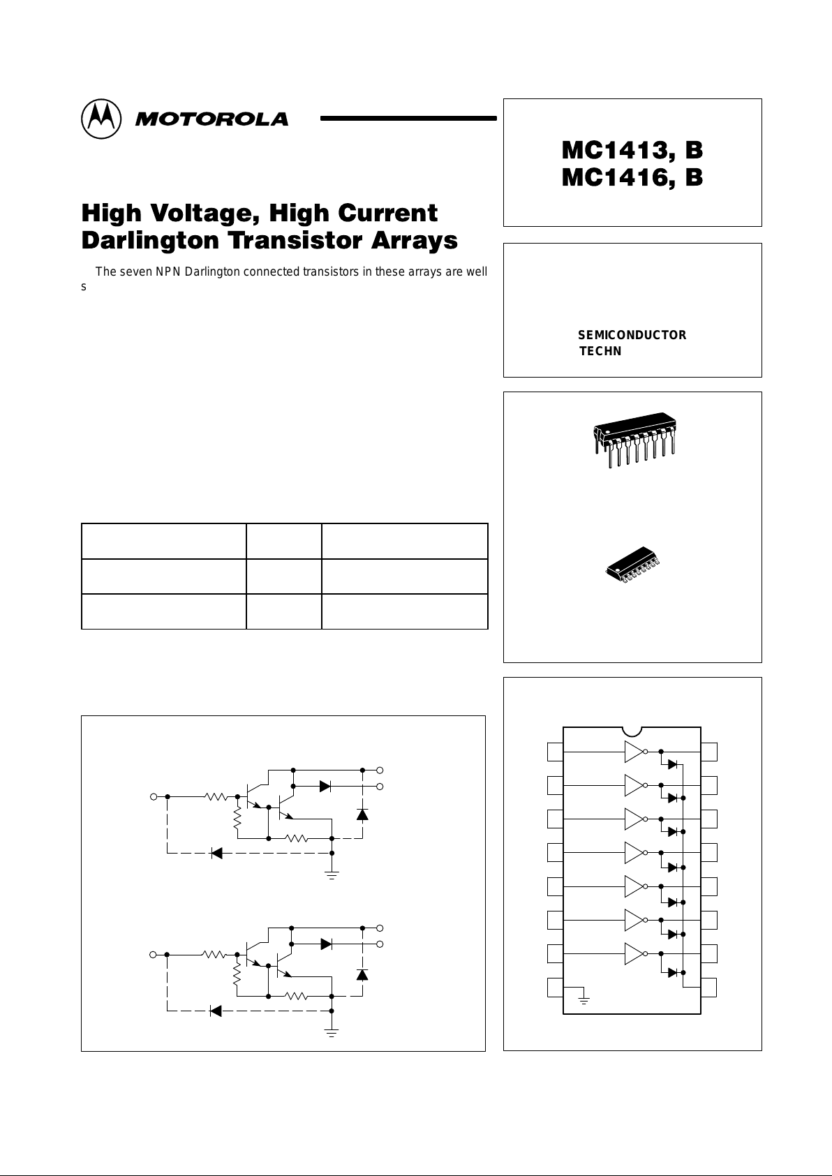
PIN CONNECTIONS
Order this document by MC1413/D
P SUFFIX
PLASTIC PACKAGE
CASE 648
D SUFFIX
PLASTIC PACKAGE
CASE 751B
(SO–16)
9
10
11
12
13
14
15
16
8
7
6
5
4
3
2
1
16
1
16
1
(Top View)
1
MOTOROLA ANALOG IC DEVICE DATA
The seven NPN Darlington connected transistors in these arrays are well
suited for driving lamps, relays, or printer hammers in a variety of industrial
and consumer applications. Their high breakdown voltage and internal
suppression diodes insure freedom from problems associated with inductive
loads. Peak inrush currents to 500 mA permit them to drive incandescent
lamps.
The MC1413, B with a 2.7 kΩ series input resistor is well suited for
systems utilizing a 5.0 V TTL or CMOS Logic. The MC1416, B uses a series
10.5 kΩ resistor and is useful in 8.0 to 18 V MOS systems.
ORDERING INFORMATION
Plastic DIP SOIC
Operating
Temperature Range
MC1413P (ULN2003A)
MC1416P (ULN2004A)
MC1413D
MC1416D
TA = –20° to +85°C
MC1413BP
MC1416BP
MC1413BD
MC1416BD
TA = –40° to +85°C
Representative Schematic Diagrams
5.0 k
10.5 k
5.0 k
3.0 k
Pin 9
Pin 9
3.0 k
1/7 MC1413, B
2.7 k
1/7 MC1416, B
Motorola, Inc. 1996 Rev 0
MC1413, B MC1416, B
2
MOTOROLA ANALOG IC DEVICE DATA
MAXIMUM RATINGS
(TA = 25°C, and rating apply to any one device in the
package, unless otherwise noted.)
Rating
Symbol Value Unit
Output Voltage V
O
50 V
Input Voltage V
I
30 V
Collector Current – Continuous I
C
500 mA
Base Current – Continuous I
B
25 mA
Operating Ambient Temperature Range
MC1413–16
MC1413B–16B
T
A
–20 to +85
–40 to +85
°C
Storage Temperature Range T
stg
–55 to +150 °C
Junction Temperature T
J
150 °C
Thermal Resistance, Junction–to–Ambient
Case 648, P Suffix
Case 751B, D Suffix
θ
JA
67
100
°C/W
NOTE: ESD data available upon request.
ELECTRICAL CHARACTERISTICS (T
A
= 25°C, unless otherwise noted)
Characteristic Symbol Min Typ Max Unit
Output Leakage Current
(VO = 50 V, TA = +85°C)
(VO = 50 V, TA = +25°C)
(VO = 50 V, TA = +85°C, VI = 1.0 V)
All Types
All Types
MC1416, B
I
CEX
–
–
–
–
–
–
100
50
500
µA
Collector–Emitter Saturation Voltage
(IC = 350 mA, IB = 500 µA)
(IC = 200 mA, IB = 350 µA)
(IC = 100 mA, IB = 250 µA)
All Types
All Types
All Types
V
CE(sat)
–
–
–
1.1
0.95
0.85
1.6
1.3
1.1
V
Input Current – On Condition
(VI = 3.85 V)
(VI = 5.0 V)
(VI = 12 V)
MC1413, B
MC1416, B
MC1416, B
I
I(on)
–
–
–
0.93
0.35
1.0
1.35
0.5
1.45
mA
Input Voltage – On Condition
(VCE = 2.0 V , IC = 200 mA)
(VCE = 2.0 V , IC = 250 mA)
(VCE = 2.0 V , IC = 300 mA)
(VCE = 2.0 V , IC = 125 mA)
(VCE = 2.0 V , IC = 200 mA)
(VCE = 2.0 V , IC = 275 mA)
(VCE = 2.0 V , IC = 350 mA)
MC1413, B
MC1413, B
MC1413, B
MC1416, B
MC1416, B
MC1416, B
MC1416, B
V
I(on)
–
–
–
–
–
–
–
–
–
–
–
–
–
–
2.4
2.7
3.0
5.0
6.0
7.0
8.0
V
Input Current – Off Condition
(IC = 500 µA, TA = 85°C)
All Types I
I(off)
50 100 – µA
DC Current Gain
(VCE = 2.0 V , IC = 350 mA)
h
FE
1000 – – –
Input Capacitance C
I
– 15 30 pF
Turn–On Delay Time
(50% EI to 50% EO)
t
on
– 0.25 1.0 µs
Turn–Off Delay Time
(50% EI to 50% EO)
t
off
– 0.25 1.0 µs
Clamp Diode Leakage Current
(VR = 50 V)
TA = +25°C
TA = +85°C
I
R
–
–
–
–
50
100
µA
Clamp Diode Forward Voltage
(IF = 350 mA)
V
F
– 1.5 2.0 V

MC1413, B MC1416, B
3
MOTOROLA ANALOG IC DEVICE DATA
1 Output Conducting at a Time
PIN 10
All Types
1
% DUTY CYCLE
VI, INPUT VOLTAGE (V)
Maximum
VI, INPUT VOLTAGE (V)
Typical
V
CE(sat)
, SATURATION VOLTAGE (V)
100
1000
700
500
300
3
10
2
4
5
6
200
10070503020
1.0
2.5
2.0
1.5
1.0
0.5
0
0
7
7.04.0 5.0 8.03.0 6.02.0
2.5
2.0
1.5
1.0
0.5
0
012117.0 8.0 9.06.0 105.0
0
100
200
400
300
500
700
600
0.4 0.6 0.8 1.0 1.2 1.4
800
1.60 0.2
I
C
, COLLECTOR CURRENT (mA)
I
I
, INPUT CURRENT (mA)
I
I
, INPUT CURRENT (mA)
I
C
, COLLECTOR CURRENT (mA)
NUMBER OF DRIVERS USED
PIN 13
All Types
100
400300 350250200150100
400
0
300
200
0
II, INPUT CURRENT (
µ
A)
50
I
O
, OUTPUT CURRENT (mA)
TYPICAL PERFORMANCE CURVES – TA = 25°C
VI, INPUT VOLTAGE (V)
0
1.0 2.0 3.0 4.0 5.0 109.08.0 11 12
400
300
200
100
0
I
O
, OUTPUT CURRENT (mA)
MC1413, B
MC1416, B
Figure 1. Output Current versus Input Voltage Figure 2. Output Current versus Input Current
Figure 3. Typical Output Characteristics Figure 4. Input Characteristics – MC1413, B
Figure 5. Input Characteristics – MC1416, B
Figure 6. Maximum Collector Current
versus Duty Cycle
(and Number of Drivers in Use)
PIN 16
Maximum
Typical

MC1413, B MC1416, B
4
MOTOROLA ANALOG IC DEVICE DATA
OUTLINE DIMENSIONS
NOTES:
1. DIMENSIONING AND TOLERANCING PER ANSI
Y14.5M, 1982.
2. CONTROLLING DIMENSION: INCH.
3. DIMENSION L TO CENTER OF LEADS WHEN
FORMED PARALLEL.
4. DIMENSION B DOES NOT INCLUDE MOLD FLASH.
5. ROUNDED CORNERS OPTIONAL.
–A–
B
F
C
S
H
G
D
J
L
M
16 PL
SEATING
18
916
K
PLANE
–T–
M
A
M
0.25 (0.010) T
DIM MIN MAX MIN MAX
MILLIMETERSINCHES
A 0.740 0.770 18.80 19.55
B 0.250 0.270 6.35 6.85
C 0.145 0.175 3.69 4.44
D 0.015 0.021 0.39 0.53
F 0.040 0.70 1.02 1.77
G 0.100 BSC 2.54 BSC
H 0.050 BSC 1.27 BSC
J 0.008 0.015 0.21 0.38
K 0.110 0.130 2.80 3.30
L 0.295 0.305 7.50 7.74
M 0 10 0 10
S 0.020 0.040 0.51 1.01
____
NOTES:
1. DIMENSIONING AND TOLERANCING PER ANSI
Y14.5M, 1982.
2. CONTROLLING DIMENSION: MILLIMETER.
3. DIMENSIONS A AND B DO NOT INCLUDE
MOLD PROTRUSION.
4. MAXIMUM MOLD PROTRUSION 0.15 (0.006)
PER SIDE.
5. DIMENSION D DOES NOT INCLUDE DAMBAR
PROTRUSION. ALLOWABLE DAMBAR
PROTRUSION SHALL BE 0.127 (0.005) TOTAL
IN EXCESS OF THE D DIMENSION AT
MAXIMUM MATERIAL CONDITION.
18
16 9
SEATING
PLANE
F
J
M
R
X 45
_
G
8 PLP
–B–
–A–
M
0.25 (0.010) B
S
–T–
D
K
C
16 PL
S
B
M
0.25 (0.010) A
S
T
DIM MIN MAX MIN MAX
INCHESMILLIMETERS
A 9.80 10.00 0.386 0.393
B 3.80 4.00 0.150 0.157
C 1.35 1.75 0.054 0.068
D 0.35 0.49 0.014 0.019
F 0.40 1.25 0.016 0.049
G 1.27 BSC 0.050 BSC
J 0.19 0.25 0.008 0.009
K 0.10 0.25 0.004 0.009
M 0 7 0 7
P 5.80 6.20 0.229 0.244
R 0.25 0.50 0.010 0.019
____
P SUFFIX
PLASTIC PACKAGE
CASE 648–08
ISSUE R
D SUFFIX
PLASTIC PACKAGE
CASE 751B–05
(SO–16)
ISSUE J
Motorola reserves the right to make changes without further notice to any products herein. Motorola makes no warranty , representation or guarantee regarding
the suitability of its products for any particular purpose, nor does Motorola assume any liability arising out of the application or use of any product or circuit, and
specifically disclaims any and all liability, including without limitation consequential or incidental damages. “T ypical” parameters which may be provided in Motorola
data sheets and/or specifications can and do vary in different applications and actual performance may vary over time. All operating parameters, including “Typicals”
must be validated for each customer application by customer’s technical experts. Motorola does not convey any license under its patent rights nor the rights of
others. Motorola products are not designed, intended, or authorized for use as components in systems intended for surgical implant into the body, or other
applications intended to support or sustain life, or for any other application in which the failure of the Motorola product could create a situation where personal injury
or death may occur. Should Buyer purchase or use Motorola products for any such unintended or unauthorized application, Buyer shall indemnify and hold Motorola
and its officers, employees, subsidiaries, affiliates, and distributors harmless against all claims, costs, damages, and expenses, and reasonable attorney fees
arising out of, directly or indirectly, any claim of personal injury or death associated with such unintended or unauthorized use, even if such claim alleges that
Motorola was negligent regarding the design or manufacture of the part. Motorola and are registered trademarks of Motorola, Inc. Motorola, Inc. is an Equal
Opportunity/Affirmative Action Employer.
How to reach us:
USA/EUROPE/Locations Not Listed: Motorola Literature Distribution; JAPAN: Nippon Motorola Ltd.; Tatsumi–SPD–JLDC, 6F Seibu–Butsuryu–Center,
P.O. Box 20912; Phoenix, Arizona 85036. 1–800–441–2447 or 602–303–5454 3–14–2 Tatsumi Koto–Ku, To kyo 135, Japan. 03–81–3521–8315
MFAX: RMF AX0@email.sps.mot.com – TOUCHT ONE 602–244–6609 ASIA/PACIFIC: Motorola Semiconductors H.K. Ltd.; 8B Tai Ping Industrial Park,
INTERNET: http://Design–NET.com 51 Ting Ko k Road, Tai Po, N.T., Hong Kong. 852–26629298
MC1413/D
*MC1413/D*
◊
 Loading...