

Motorola MC141531T, MC141531Z Datasheet
3–139
MC141531MOTOROLA
Advance Information
LCD Segment / Common Driver
CMOS
MC141531 is a CMOS LCD Driver which consists of 3 annunciator outputs and 137 high voltage LCD driving signals (17 common and 120 segment). It has parallel interface capability for operating with general MCU.
Besides the general LCD driver features, it has on chip LCD bias voltage
generator circuits such that limited external component is required during
application.
• Single Supply Operation, 2.4 V - 3.5 V
• Operating Temperature Range : -30˚C to 85˚C
• Low Current Stand-by Mode (<500nA)
• On Chip Bias DC/DC Converter
• 8 bit Parallel Interface
• Graphic Mode Operation
• On Chip 120x17 Graphic Display Data RAM
• Master clear RAM
• 120 Segment Drivers, 17 Common Drivers
• 1/16, 1/17 Multiplex Ratio
• 1:5 bias ratio
• Re-mapping of Row and Column Drivers
• Three Stand Alone Annunciator (Static Icon) Driver Circuits
• Low Power Icon Mode Driven by Com16 in Special Driving Scheme
• Selectable LCD Drive Voltage Temperature Coefficients
• 16 level Internal Contrast Control
• External Contrast Control
• Standard TAB (Tape Automated Bonding) Package, Gold Bump Die
MC141531
ORDERING INFORMATION
MC141531T TAB
MCC141531Z Gold Bump Die
This document contains information on a new product. Specifications and information herein are subject to change without notice.
MC141531T
TAB
MCC141531Z
Gold Bump Die
MOTOROLA
SEMICONDUCTOR TECHNICAL DATA
REV 4
3/97
MOTOROLA
3–140
MC141531
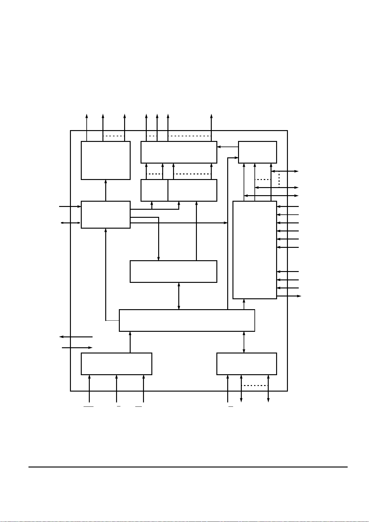
LCD Driving
DC/DC Converter
Tripler,
Doubler,
Voltage Regulator,
Voltage Divider,
Contrast Control,
Temperature
Compensation
BP
Annun0
to
Annun2
Com0 to
Com16
Seg0~Seg119
Annunciator
Control
Circuit
OSC1
OSC2
DVSS
DVDD
RES R/W D0~D7
VLL6
VLL2
VCC
VR
VF
C2P
C2N
C1P
C1N
C+
CAVDD
AVSS
GDDRAM
17 x 120Bits
Command Decoder
Parallel InterfaceCommand Interface
Display
Timing
Generator
120 Bit Latch
17 Bit
Latch
HV Buffer Cell Level Shifter
Level
Selector
CS (CLK)
D/
C
Block Diagram
3–141
MC141531MOTOROLA
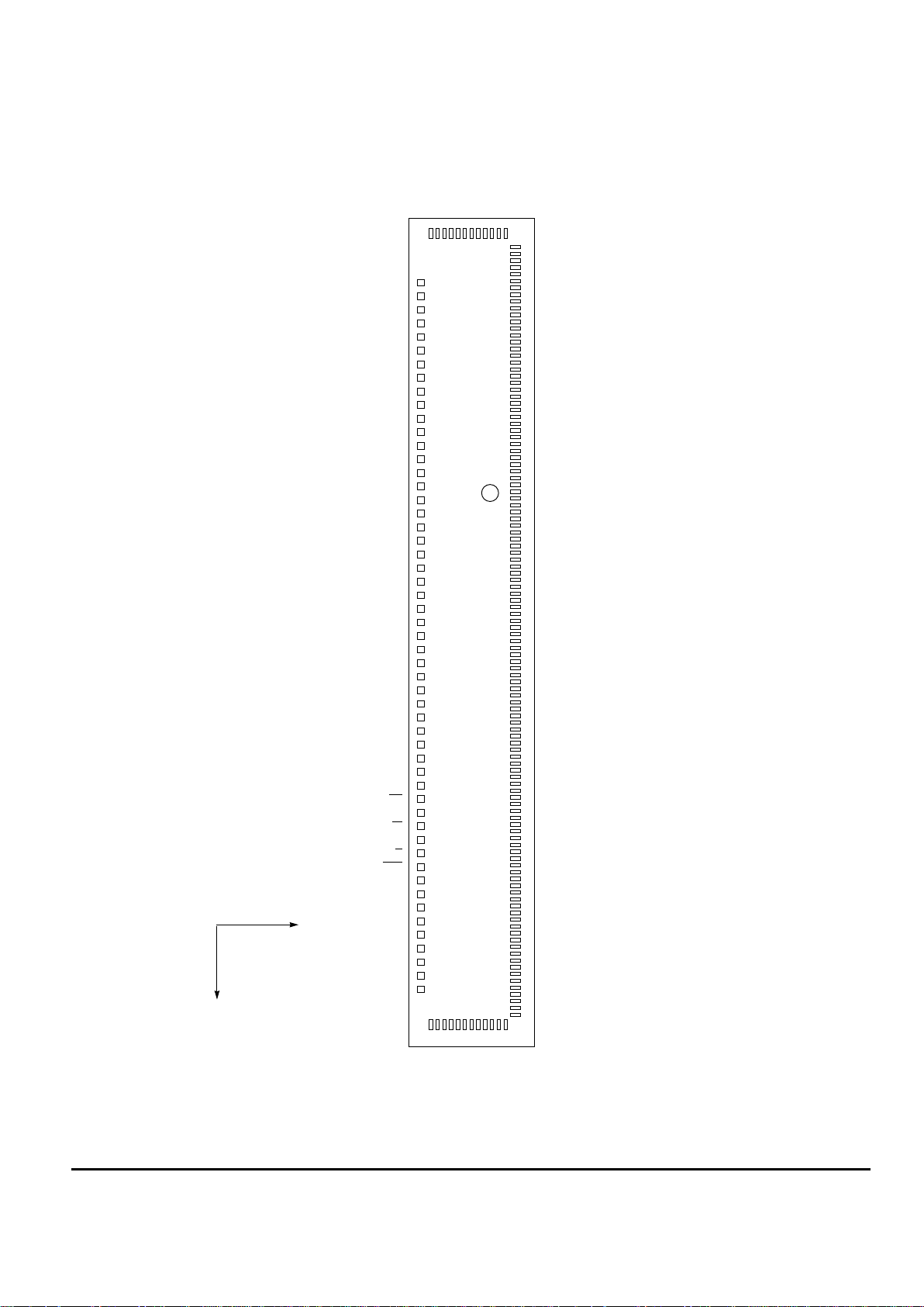
MC141531T PIN ASSIGNMENT
(COPPER VIEW)
12345678910111213141516171819202122232425262728293031
32
DUMMY
DUMMY
DUMMY
DUMMY
OSC2
AVSS
VR
VF
VCC
C-
C+
VLL6
VLL5
VLL4
OSC1
VLL3
VLL2
C1N
C1P
C2N
C2P
AVDD
D7D6D5D4D3D2D1
D0
DVSS
CS (CLK)
R/W
D/C
RES
DVDD
COM16
COM0
COM1
COM2
COM3
COM4.......COM13
COM14
COM15
COM16
SEG0
SEG1
SEG2
SEG3
SEG4........................
SEG117
SEG118
SEG119
ANNUN0
ANNUN1
ANNUN2
BP
174
173
172
171
170
169
.......
160
159
158
157
156
155
154
153
152
.......................
.
39383736353433
MOTOROLA
3–142
MC141531
MC141531 Die Pin Assignment
OSC2
AVSS
VR
VF
VCC
C-
C+
VLL6
VLL5
VLL4
OSC1
VLL3
VLL2
C1N
C1P
C2N
C2P
AVDD
AVDD
DVSS
DVSS
DVSS
D7
DVSS
D6
DVSS
D5
DVSS
D4
DVSS
D3
DVSS
D2
DVSS
D1
DVSS
D0
DVSS
CS
DVSS
R/
W
DVSS
D/
C
RES
DVDD
BP
DVSS
ANNUN2
DVSS
ANNUN1
DVSS
ANNUN0
DVSS
COM11
COM12
COM13
COM14
COM15
COM16
SEG0
SEG1
SEG2
SEG3
SEG4
SEG5
SEG6
SEG7
SEG8
SEG9
SEG10
SEG11
SEG12
SEG13
SEG14
SEG15
SEG16
SEG17
SEG18
SEG19
SEG20
SEG21
SEG22
SEG23
SEG24
SEG25
SEG26
SEG27
SEG28
SEG29
SEG30
SEG31
SEG32
SEG33
SEG34
SEG35
SEG36
SEG37
SEG38
SEG39
SEG40
SEG41
SEG42
SEG43
SEG44
SEG45
SEG46
SEG47
SEG48
SEG49
SEG50
SEG51
SEG52
SEG53
SEG54
SEG55
SEG56
SEG57
SEG58
SEG59
SEG60
SEG61
SEG62
SEG63
SEG64
SEG65
SEG66
SEG67
SEG68
SEG69
SEG70
SEG71
SEG72
SEG73
SEG74
SEG75
SEG76
SEG77
SEG78
SEG79
SEG80
SEG81
SEG82
SEG83
SEG84
SEG85
SEG86
SEG87
SEG88
SEG89
SEG90
SEG91
SEG92
SEG93
SEG94
SEG95
SEG96
SEG97
SEG98
SEG99
SEG100
SEG101
SEG102
SEG103
SEG104
SEG105
SEG106
SEG107
SEG108
SEG109
SEG110
SEG111
SEG112
SEG113
SEG114
SEG115
SEG116
SEG117
SEG118
SEG119
COM10
COM9
COM8
COM7
COM6
COM5
COM4
COM3
COM2
COM1
COM0
COM16
Y
X
M
1
53
54
65
66
179
180
191
3–143
MC141531MOTOROLA
MAXIMUM RATINGS* (Voltages Referenced to V
SS
, TA=25˚C)
Symbol Parameter Value Unit
AV
DD
,DV
DD
Supply Voltage -0.3 to +4.0 V
V
CC
VSS-0.3 to VSS+10.5 V
V
in
Input Voltage VSS-0.3 to VDD+0.3 V
I Current Drain Per Pin Excluding VDD and V
SS
25 mA
T
A
Operating Temperature -30 to +85 ˚C
T
stg
Storage Temperature Range -65 to +150 ˚C
* Maximum Ratings are those values beyond which damage to the device may occur. Functional
operation should be restricted to the limits in the Electrical Characteristics tables or Pin Description section.
VSS = AVSS = DVSS (DVSS = VSS of Digital circuit, AVSS = VSS of Analogue Circuit)
VDD = AVDD = DVDD (DVDD = VDD of Digital circuit, AVDD = VDD of Analogue Circuit)
This device contains circuitry to protect the inputs
against damage due to high static voltages or electric fields; however, it is advised that normal precautions to be taken to avoid application of any voltage
higher than maximum rated voltages to this high
impedance circuit. For proper operation it is recommended that Vin and V
out
be constrained to the
range VSS < or = (Vin or V
out
) < or = VDD. Reliability
of operation is enhanced if unused input are connected to an appropriate logic voltage level (e.g.,
either VSS or VDD). Unused outputs must be left
open. This device may be light sensitive. Caution
should be taken to avoid exposure of this device to
any light source during normal operation. This
device is not radiation protected.
ELECTRICAL CHARACTERISTICS (Voltage Referenced to VSS, VDD=2.4 to 3.5V, TA=25˚C)
Symbol Parameter Test Condition Min Typ Max Unit
DV
DD
AV
DD
Logic Circuit Supply Voltage Range
DC/DC Converter Circuit Supply Voltage Range
(Absolute value referenced to VSS) 2.4
2.4
3.0
-
3.5
3.5
V
V
I
AC
I
DP
I
SB1
I
SB2
I
SB3
Access Mode Supply Current Drain
(AVDD + DVDD Pins)
Display Mode Supply Current Drain
(AVDD + DVDD Pins)
Standby Mode Supply Current Drain
(AVDD + DVDD Pins)
Annunciator Mode Supply Current Drain
(AVDD + DVDD Pins)
Icon Mode Supply Current Drain
(AVDD + DVDD Pins)
VDD=3.0V, Internal DC/DC Converter On, Tripler
Enabled, Annunciator On/Off, R/W accessing,
T
cyc
=1MHz, Osc. Freq.=38.4kHz, Display On, 1/7
Mux Ratio
VDD=3.0V, Internal DC/DC Converter On, Tripler
Enabled,
Annunciator On/Off, R/W halt, Osc. Freq.=38.4kHz,
Display On, 1/17Mux Ratio
VDD=3.0V, Display off, Oscillator Disabled, R/W halt.
VDD=3.0V, Annunciator Mode, Internal Oscillator,
Oscillator Enabled, Display Off, R/W halt, Int Osc.
Freq.=38.4kHz.
VDD=3.0V, Icon Mode, Internal Oscillator, Oscillator
Enabled, Display Off, R/W halt, Ext Osc.
Freq.=38.4kHz.
0
0
0
0
0
200
75
300
5
-
300
165
500
10
25
µA
µA
nA
µA
µA
V
CC1
V
CC2
V
LCD
LCD Driving DC/DC Converter Output
(VCC Pin)
LCD Driving DC/DC Converter Output
(VCC Pin)
LCD Driving Voltage Input (VCC Pin)
Display On, Internal DC/DC Converter Enabled,
Tripler Enabled, Osc. Freq.=38.4KHz,
Regulator Enabled, Divider Enabled.
Display On, Internal DC/DC Converter Enabled,
Doubler Enabled, Osc. Freq.=38.4KHz,
Regulator Enabled, Divider Enabled.
Internal DC/DC Converter Disabled.
-
-
5
3*AV
DD
2*AV
DD
-
10.5
7
10.5
V
V
V
MOTOROLA
3–144
MC141531
TC(%)=
VR at 50˚C - VR at 0˚C
50˚C - 0˚C
X
1
VR at 25˚C
X100%
ELECTRICAL CHARACTERISTICS (Voltage Referenced to VSS, VDD=2.4 to 3.5V, TA=25˚C)
*The formula for the temperature coefficient (TC) is:
Symbol Parameter Test Condition Min Typ Max Unit
V
IH1
V
IL1
Input high voltage
(RES, OSC2, CS, D0-D7, R/W, D/C, OSC1)
Input Low voltage
(RES, OSC2, CS, D0-D7, R/W, D/C, OSC1)
0.8*V
DD
0
-
-
V
DD
0.2*V
DD
V
V
V
LL6
V
LL5
V
LL4
V
LL3
V
LL2
V
LL6
V
LL5
V
LL4
V
LL3
V
LL2
LCD Display Voltage Output
(V
LL6
, V
LL5
, V
LL4
, V
LL3
, V
LL2
Pins)
LCD Display Voltage Input
(V
LL6
, V
LL5
, V
LL4
, V
LL3
, V
LL2
Pins)
Voltage Divider Enabled
External DC/DC Converter, Voltage Divider Disable
-
-
-
-
-
5
0
0
0
0
V
R
0.8*V
R
0.6*V
R
0.4*V
R
0.2*V
R
-
-
-
-
-
-
-
-
-
-
V
CC
V
LL6
V
LL5
V
LL4
V
LL3
V
V
V
V
V
V
V
V
V
V
I
OH
I
OL
I
OZ
Output High Current Source
(D0-D7, Annun0-2, BP, OSC2)
Output Low Current Drain
(D0-D7, Annun0-2, BP, OSC2)
Output Tri-state Current Drain Source
(D0-D7, OSC2)
V
out=VDD
-0.4V
V
out
=0.4V
50
-
-1
-
-
-
-
-50
1
µA
µA
µA
IIL/IIHInput Current
(RES, OSC2, CS, D0-D7, R/W, D/C , OSC1)
-1 - 1 µA
R
on
Channel resistance between LCD driving signal
pins (SEG and COM) and driving voltage input
pins (V
LL2
to V
LL6
)
During Display on, 0.1V apply between two terminals, VCC within operating voltage range
- - 10 kΩ
V
SB
Memory Retention Voltage (DVDD) Standby mode, retain all internal configuration and
RAM data
2--V
CINInput Capacitance
(OSC1, OSC2, all logic pins)
- 5 7.5 pF
PTC0
PTC1
PTC2
PTC3
Temperature Coefficient Compensation*
Flat Temperature Coefficient
Temperature Coefficient 1*
Temperature Coefficient 2*
Temperature Coefficient 3*
TC1=0, TC2=0, Voltage Regulator Disabled
TC1=0, TC2=1, Voltage Regulator Enabled
TC1=1, TC2=0, Voltage Regulator Enabled
TC1=1, TC2=1, Voltage Regulator Enabled
-
-
-
-
0.0
-0.18
-0.22
-0.35
-
-
-
-
%
%
%
%
V
CN
Internal Contrast Control
(VR Output Voltage)
Regulator Enabled, Internal Contrast control
Enabled. (16 Voltage Levels Controlled by Software.
Each level is typically 2.25% of the Regulator Output
Voltage. )
- ± 18 - %
3–145
MC141531MOTOROLA
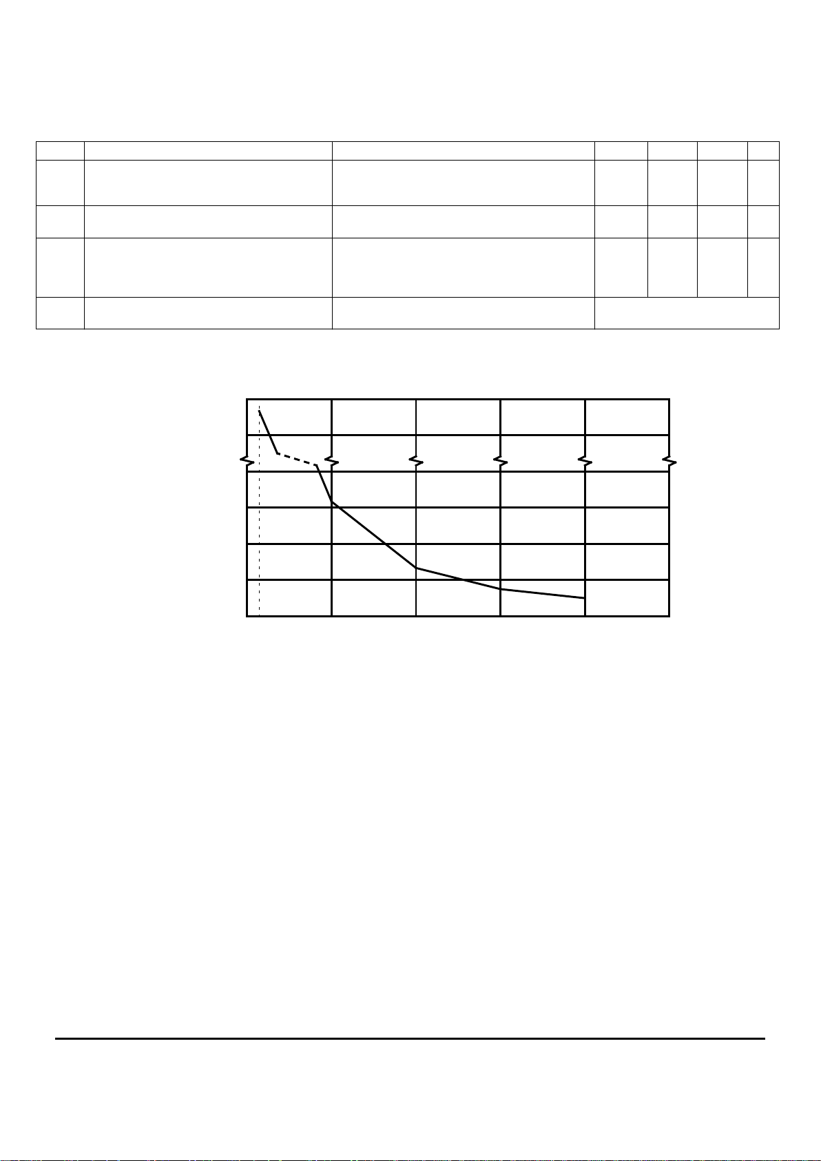
Figure 1. Internal Oscillator Frequency Relationship with External Resistor Value
100k 500k 1.0M 1.5M 2.0M
Resistor Value between OSC1 and OSC2 (Ω)
Oscillation
Frequency
(Hz)
260k
90k
70k
50k
30k
10k
280k
AC ELECTRICAL CHARACTERISTICS (TA=25˚C, Voltage referenced to VSS, AVDD=DVDD=3V)
Note: F
FRM
= F
OSC
/ 640
F
ANN
= F
OSC
/ 1280
Symbol Parameter Test Condition Min Typ Max Unit
F
OSC
Oscillation Frequency of Display timing generator 60Hz Frame Frequency
Either External Clock Input or Internal Oscillator
Enabled
- 38.4 - kHz
F
ANN
Backplane Frequency of Annunciator
(Annun0-3, BP)
50% duty cycle
Annunciator on, Fosc=38.4KHz
-30-Hz
F
FRM
Frame Frequency Graphic Display Mode,
Timing generator freq. = 38.4kHz
Icon Mode, Timing generator freq. = 38.4kHz
-60
TBD
-Hz
OSC Internal Oscillation Frequency with different value
of feedback resistor
Internal Oscillator Enabled, VDD within operation
range
See Figure 1 for the relationship
MOTOROLA
3–146
MC141531
Valid Data
t
cycle
t
EH
t
AS
t
AH
t
DH
t
DS
CS
R/W
D/C
D0-D7
TABLE 2a. Parallel Timing Characteristics (Write Cycle) (TA=-30 to 85˚C, DVDD=2.4 to 3.5V, VSS=0V)
Symbol Parameter Min Typ Max Unit
t
cycle
Enable Cycle Time 600 - - ns
t
EH
Enable Pulse Width 290 - - ns
t
AS
Address Setup Time 5 - - ns
t
DS
Data Setup Time 290 - - ns
t
DH
Data Hold Time 20 - - ns
t
AH
Address Hold Time 20 - - ns
Figure 3. Timing Characteristics (Write Cycle)
 Loading...