

查询MCC141531Z供应商
MOTOROLA
SEMICONDUCTOR TECHNICAL DATA
Advance Information
LCD Segment / Common Driver
CMOS
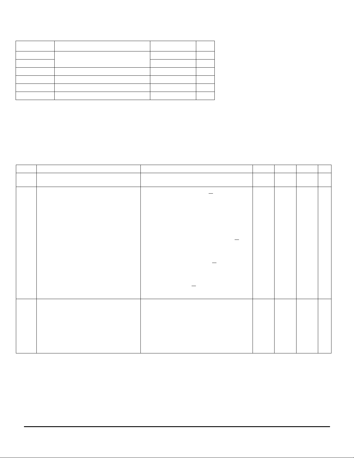
MC141531 is a CMOS LCD Driver which consists of 3 annunciator outputs and 137 high voltage LCD driving signals (17 common and 120 segment). It has parallel interface capability for operating with general MCU.
Besides the general LCD driver features, it has on chip LCD bias voltage
generator circuits such that limited external component is required during
application.
• Single Supply Operation, 2.4 V - 3.5 V
• Operating Temperature Range : -30˚C to 85˚C
• Low Current Stand-by Mode (<500nA)
• On Chip Bias DC/DC Converter
• 8 bit Parallel Interface
• Graphic Mode Operation
• On Chip 120x17 Graphic Display Data RAM
• Master clear RAM
• 120 Segment Drivers, 17 Common Drivers
• 1/16, 1/17 Multiplex Ratio
• 1:5 bias ratio
• Re-mapping of Row and Column Drivers
• Three Stand Alone Annunciator (Static Icon) Driver Circuits
• Low Power Icon Mode Driven by Com16 in Special Driving Scheme
• Selectable LCD Drive Voltage Temperature Coefficients
• 16 level Internal Contrast Control
• External Contrast Control
• Standard TAB (Tape Automated Bonding) Package, Gold Bump Die
MC141531
MC141531T
TAB
MCC141531Z
Gold Bump Die
ORDERING INFORMATION
MC141531T TAB
MCC141531Z Gold Bump Die
REV 4
3/97
This document contains information on a new product. Specifications and information herein are subject to change without notice.
MC141531MOTOROLA
3–139
BP
Annun0
to
Annun2
Com0 to
Com16
Block Diagram
Seg0~Seg119
OSC1
OSC2
Annunciator
Control
Circuit
Display
Timing
Generator
HV Buffer Cell Level Shifter
17 Bit
Latch
120 Bit Latch
GDDRAM
17 x 120Bits
Command Decoder
Level
Selector
LCD Driving
DC/DC Converter
Tripler,
Doubler,
Voltage Regulator,
Voltage Divider,
Contrast Control,
Temperature
Compensation
VLL6
VLL2
VCC
VR
VF
C2P
C2N
C1P
C1N
C+
CAVDD
AVSS
DVSS
DVDD
MC141531
3–140
Parallel InterfaceCommand Interface
C
RES R/W D0~D7
D/
CS (CLK)
MOTOROLA
DUMMY
COM16
174
COM0
COM1
COM2
COM3
COM4.......COM13
172
171
.......
170
169
173
160
COM14
COM15
159
158
COM16
SEG0
157
156
SEG1
SEG2
SEG3
SEG4........................
.......................
155
154
153
152
SEG117
SEG118
SEG119
ANNUN0
.
39383736353433
ANNUN1
ANNUN2
BP
DUMMY
12345678910111213141516171819202122232425262728293031
C-
OSC2
DUMMY
VR
AVSS
VF
VCC
C+
VLL6
VLL5
VLL4
VLL3
OSC1
VLL2
C1N
C1P
D7D6D5D4D3D2D1
C2P
C2N
AVDD
D0
DVSS
CS (CLK)
MC141531T PIN ASSIGNMENT
(COPPER VIEW)
R/W
D/C
RES
32
DVDD
DUMMY
MC141531MOTOROLA
3–141
MC141531 Die Pin Assignment
COM5
COM4
SEG113
SEG114
COM7
COM6
SEG111
SEG112
COM8
M
SEG110
COM10
COM9
SEG108
SEG109
65
180
179
COM11
COM12
COM13
COM14
COM15
COM16
SEG0
SEG1
SEG2
SEG3
SEG4
SEG5
SEG6
SEG7
SEG8
SEG9
SEG10
SEG11
SEG12
SEG13
SEG14
SEG15
SEG16
SEG17
SEG18
SEG19
SEG20
SEG21
SEG22
SEG23
SEG24
SEG25
SEG26
SEG27
SEG28
SEG29
SEG30
SEG31
SEG32
SEG33
SEG34
SEG35
SEG36
SEG37
SEG38
SEG39
SEG40
SEG41
SEG42
SEG43
SEG44
SEG45
SEG46
SEG47
SEG48
SEG49
SEG50
SEG51
SEG52
SEG53
SEG54
SEG55
SEG56
SEG57
SEG58
SEG59
SEG60
SEG61
SEG62
SEG63
SEG64
SEG65
SEG66
SEG67
SEG68
SEG69
SEG70
SEG71
SEG72
SEG73
SEG74
SEG75
SEG76
SEG77
SEG78
SEG79
SEG80
SEG81
SEG82
SEG83
SEG84
SEG85
SEG86
SEG87
SEG88
SEG89
SEG90
SEG91
SEG92
SEG93
SEG94
SEG95
SEG96
SEG97
SEG98
SEG99
SEG100
SEG101
SEG102
SEG103
SEG104
SEG105
SEG106
SEG107
66
COM16
COM3
COM2
COM1
COM0
191
1
OSC2
AVSS
VR
VF
VCC
C-
C+
VLL6
VLL5
VLL4
OSC1
VLL3
VLL2
C1N
C1P
C2N
C2P
AVDD
AVDD
DVSS
DVSS
DVSS
D7
DVSS
D6
DVSS
D5
DVSS
D4
DVSS
D3
DVSS
D2
DVSS
D1
DVSS
D0
DVSS
CS
DVSS
W
R/
DVSS
C
D/
RES
DVDD
BP
DVSS
Y
ANNUN2
DVSS
ANNUN1
DVSS
ANNUN0
DVSS
X
53
54
SEG115
SEG116
SEG117
SEG118
SEG119
MC141531
3–142
MOTOROLA
MAXIMUM RATINGS* (Voltages Referenced to V
, TA=25˚C)
SS
Symbol Parameter Value Unit
AV
,DV
DD
V
CC
V
in
I Current Drain Per Pin Excluding VDD and V
T
A
T
stg
Supply Voltage -0.3 to +4.0 V
DD
VSS-0.3 to VSS+10.5 V
Input Voltage VSS-0.3 to VDD+0.3 V
SS
25 mA
Operating Temperature -30 to +85 ˚C
Storage Temperature Range -65 to +150 ˚C
This device contains circuitry to protect the inputs
against damage due to high static voltages or electric fields; however, it is advised that normal precautions to be taken to avoid application of any voltage
higher than maximum rated voltages to this high
impedance circuit. For proper operation it is recommended that Vin and V
range VSS < or = (Vin or V
be constrained to the
out
) < or = VDD. Reliability
out
of operation is enhanced if unused input are connected to an appropriate logic voltage level (e.g.,
either VSS or VDD). Unused outputs must be left
open. This device may be light sensitive. Caution
should be taken to avoid exposure of this device to
* Maximum Ratings are those values beyond which damage to the device may occur. Functional
operation should be restricted to the limits in the Electrical Characteristics tables or Pin Descrip-
any light source during normal operation. This
device is not radiation protected.
tion section.
VSS = AVSS = DVSS (DVSS = VSS of Digital circuit, AVSS = VSS of Analogue Circuit)
VDD = AVDD = DVDD (DVDD = VDD of Digital circuit, AVDD = VDD of Analogue Circuit)
ELECTRICAL CHARACTERISTICS (Voltage Referenced to VSS, VDD=2.4 to 3.5V, TA=25˚C)
Symbol Parameter Test Condition Min Typ Max Unit
DV
AV
Logic Circuit Supply Voltage Range
DD
DC/DC Converter Circuit Supply Voltage Range
DD
I
Access Mode Supply Current Drain
AC
(AVDD + DVDD Pins)
I
Display Mode Supply Current Drain
DP
(AVDD + DVDD Pins)
I
Standby Mode Supply Current Drain
SB1
(AVDD + DVDD Pins)
(Absolute value referenced to VSS) 2.4
2.4
VDD=3.0V, Internal DC/DC Converter On, Tripler
Enabled, Annunciator On/Off, R/W accessing,
T
=1MHz, Osc. Freq.=38.4kHz, Display On, 1/7
cyc
Mux Ratio
VDD=3.0V, Internal DC/DC Converter On, Tripler
Enabled,
Annunciator On/Off, R/W halt, Osc. Freq.=38.4kHz,
Display On, 1/17Mux Ratio
VDD=3.0V, Display off, Oscillator Disabled, R/W halt.
3.0
-
0
0
0
200
75
300
3.5
3.5
300
165
500
V
V
µA
µA
nA
V
V
V
I
Annunciator Mode Supply Current Drain
SB2
(AVDD + DVDD Pins)
I
Icon Mode Supply Current Drain
SB3
(AVDD + DVDD Pins)
LCD Driving DC/DC Converter Output
CC1
(VCC Pin)
LCD Driving DC/DC Converter Output
CC2
(VCC Pin)
LCD Driving Voltage Input (VCC Pin)
LCD
VDD=3.0V, Annunciator Mode, Internal Oscillator,
Oscillator Enabled, Display Off, R/W halt, Int Osc.
Freq.=38.4kHz.
VDD=3.0V, Icon Mode, Internal Oscillator, Oscillator
Enabled, Display Off, R/W halt, Ext Osc.
Freq.=38.4kHz.
Display On, Internal DC/DC Converter Enabled,
Tripler Enabled, Osc. Freq.=38.4KHz,
Regulator Enabled, Divider Enabled.
Display On, Internal DC/DC Converter Enabled,
Doubler Enabled, Osc. Freq.=38.4KHz,
Regulator Enabled, Divider Enabled.
Internal DC/DC Converter Disabled.
0
0
-
-
5
3*AV
2*AV
5
-
-
DD
DD
10
25
10.5
7
10.5
µA
µA
V
V
V
MC141531MOTOROLA
3–143
ELECTRICAL CHARACTERISTICS (Voltage Referenced to VSS, VDD=2.4 to 3.5V, TA=25˚C)
Symbol Parameter Test Condition Min Typ Max Unit
V
Input high voltage
IH1
0.8*V
DD
-
V
DD
(RES, OSC2, CS, D0-D7, R/W, D/C, OSC1)
V
Input Low voltage
IL1
0
-
0.2*V
DD
(RES, OSC2, CS, D0-D7, R/W, D/C, OSC1)
V
LCD Display Voltage Output
LL6
V
LL5
V
LL4
V
LL3
V
LL2
V
LL6
V
LL5
V
LL4
V
LL3
V
LL2
I
OH
(V
, V
LL5
, V
LL4
LL6
LCD Display Voltage Input
(V
, V
LL5
, V
LL4
LL6
Output High Current Source
(D0-D7, Annun0-2, BP, OSC2)
I
Output Low Current Drain
OL
(D0-D7, Annun0-2, BP, OSC2)
I
Output Tri-state Current Drain Source
OZ
(D0-D7, OSC2)
IIL/IIHInput Current
, V
, V
LL3
LL3
, V
, V
LL2
LL2
Pins)
Pins)
Voltage Divider Enabled
External DC/DC Converter, Voltage Divider Disable
V
V
out=VDD
=0.4V
out
-0.4V
-
-
-
-
-
5
0
0
0
0
50
-
-1
V
0.8*V
0.6*V
0.4*V
0.2*V
-
-
-
-
-
-
-
-
R
-
-
R
-
R
-
R
-
R
V
CC
V
LL6
V
LL5
V
LL4
V
LL3
-
-50
1
-1 - 1 µA
(RES, OSC2, CS, D0-D7, R/W, D/C , OSC1)
R
Channel resistance between LCD driving signal
on
pins (SEG and COM) and driving voltage input
pins (V
V
Memory Retention Voltage (DVDD) Standby mode, retain all internal configuration and
SB
LL2
to V
LL6
)
During Display on, 0.1V apply between two terminals, VCC within operating voltage range
- - 10 kΩ
2--V
RAM data
CINInput Capacitance
- 5 7.5 pF
(OSC1, OSC2, all logic pins)
Temperature Coefficient Compensation*
PTC0
PTC1
PTC2
PTC3
V
CN
Flat Temperature Coefficient
Temperature Coefficient 1*
Temperature Coefficient 2*
Temperature Coefficient 3*
Internal Contrast Control
(VR Output Voltage)
TC1=0, TC2=0, Voltage Regulator Disabled
TC1=0, TC2=1, Voltage Regulator Enabled
TC1=1, TC2=0, Voltage Regulator Enabled
TC1=1, TC2=1, Voltage Regulator Enabled
Regulator Enabled, Internal Contrast control
Enabled. (16 Voltage Levels Controlled by Software.
-
-
-
-
0.0
-0.18
-0.22
-0.35
-
-
-
-
- ± 18 - %
Each level is typically 2.25% of the Regulator Output
Voltage. )
*The formula for the temperature coefficient (TC) is:
V
V
V
V
V
V
V
V
V
V
V
V
µA
µA
µA
%
%
%
%
TC(%)=
VR at 50˚C - VR at 0˚C
50˚C - 0˚C
MC141531
3–144
X
VR at 25˚C
1
X100%
MOTOROLA
AC ELECTRICAL CHARACTERISTICS (TA=25˚C, Voltage referenced to VSS, AVDD=DVDD=3V)
Symbol Parameter Test Condition Min Typ Max Unit
F
F
F
Oscillation Frequency of Display timing generator 60Hz Frame Frequency
OSC
Either External Clock Input or Internal Oscillator
Enabled
Backplane Frequency of Annunciator
ANN
(Annun0-3, BP)
Frame Frequency Graphic Display Mode,
FRM
50% duty cycle
Annunciator on, Fosc=38.4KHz
Timing generator freq. = 38.4kHz
- 38.4 - kHz
-30-Hz
-60
-Hz
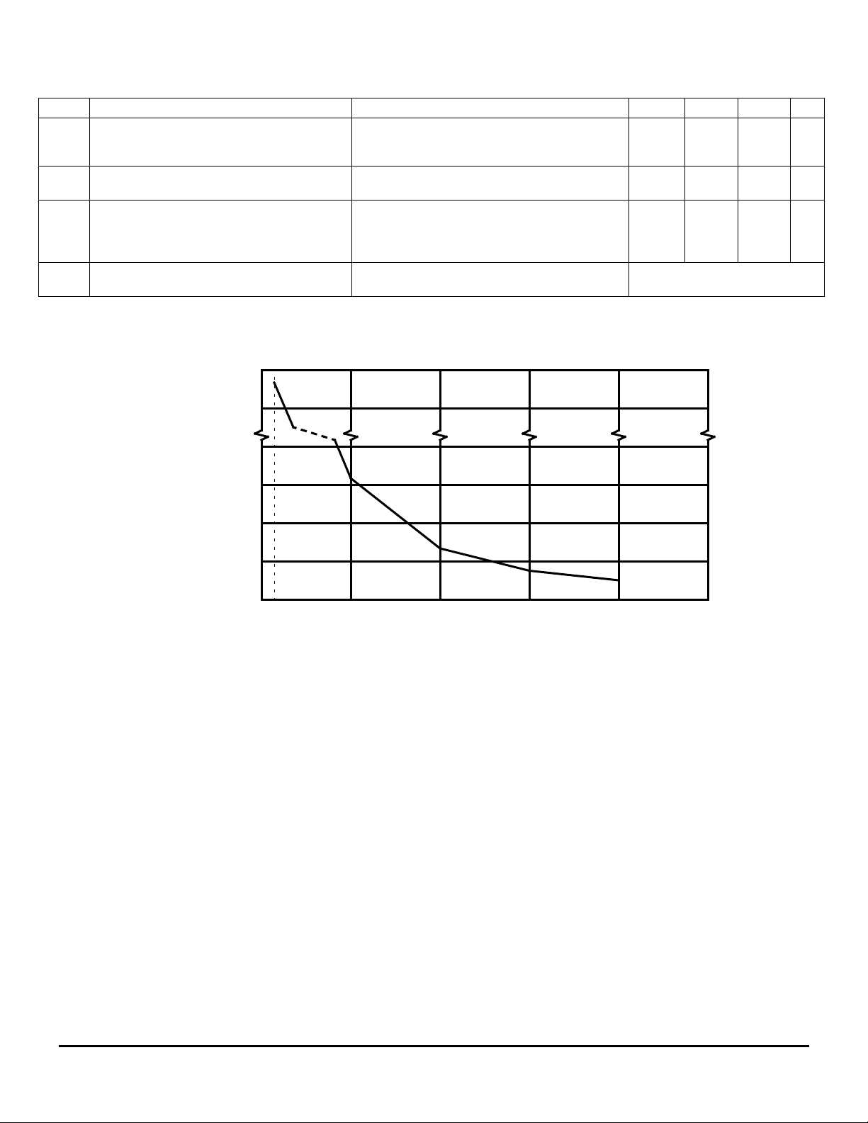
OSC Internal Oscillation Frequency with different value
of feedback resistor
Note: F
F
FRM
ANN
= F
= F
OSC
OSC
/ 640
/ 1280
280k
260k
90k
70k
Oscillation
Frequency
(Hz)
50k
30k
10k
100k 500k 1.0M 1.5M 2.0M
Figure 1. Internal Oscillator Frequency Relationship with External Resistor Value
Icon Mode, Timing generator freq. = 38.4kHz
Internal Oscillator Enabled, VDD within operation
range
Resistor Value between OSC1 and OSC2 (Ω)
TBD
See Figure 1 for the relationship
MC141531MOTOROLA
3–145
TABLE 2a. Parallel Timing Characteristics (Write Cycle) (TA=-30 to 85˚C, DVDD=2.4 to 3.5V, VSS=0V)
Symbol Parameter Min Typ Max Unit
t
cycle
t
EH
t
AS
t
DS
t
DH
t
AH
Enable Cycle Time 600 - - ns
Enable Pulse Width 290 - - ns
Address Setup Time 5 - - ns
Data Setup Time 290 - - ns
Data Hold Time 20 - - ns
Address Hold Time 20 - - ns
t
cycle
CS
t
EH
R/W
D/C
D0-D7
t
AS
t
DS
Valid Data
Figure 3. Timing Characteristics (Write Cycle)
t
AH
t
DH
MC141531
3–146
MOTOROLA

TABLE 2b. Parallel Timing Characteristics (Read Cycle) (TA=-30 to 85˚C, DVDD=2.4 to 3.5V, VSS=0V)
Symbol Parameter Min Typ Max Unit
t
cycle
t
EH
t
AS
t
DS
t
DH
t
AH
Enable Cycle Time 600 - - ns
Enable Pulse Width 290 - - ns
Address Setup Time 5 - - ns
Data Setup Time - - 290 ns
Data Hold Time 5 - - ns
Address Hold Time 20 - - ns
t
cycle
CS
t
EH
R/W
D/C
D0-D7
t
AS
t
DS
Valid Data
Figure 4. Timing Characteristics (Read Cycle)
t
AH
t
DH
MC141531MOTOROLA
3–147

PIN DESCRIPTIONS
D/C (Data / Command)
This input pin tell the LCD driver the input at D0-D7 is data or com-
mand. Input High for data while input Low for command.
CS (CLK) (Input Clock)
This pin is normal Low clock input. Data on D0-D7 are latched at
the falling edge of CS.
RES (Reset)
An active Low pulse to this pin reset the internal status of the
driver (same as power on reset). The minimum pulse width is 10 µs.
D0-D7 (Data)
This bi-directional bus is used for data / command transferring.
R/W (Read / Write)
This is an input pin. To read the display data RAM or the internal
status (Busy / Idle), pull this pin High. The R/W input Low indicates a
write operation to the display data RAM or to the internal setup registers.
OSC1 (Oscillator Input)
For internal oscillator mode, this is an input for the internal low
power RC oscillator circuit. In this mode, an external resistor of certain value should be connected between the OSC1 and OSC2 pins
for a range of internal operating frequencies (refer to Figure 1). For
external oscillator mode, OSC1 should be left open.
OSC2 (Oscillator Output / External Oscillator Input)
For internal oscillator mode, this is an output for the internal low
power RC oscillator circuit. For external oscillator mode, OSC2 will
be an input pin for external clock and no external resistor is needed.
VLL6 - VLL2
Group of voltage level pins for driving the LCD panel. They can
either be connected to external driving circuit for external bias supply
or connected internally to built-in divider circuit if internal divider is
enable. For Internal DC/DC Converter enabled, a 0.1 µF capacitor to
AVSSis required on each pin.
C1N and C1P
If Internal DC/DC Converter is enabled, a 0.1 µF capacitor is
required to connect these two pins.
C2N and C2P
If Internal DC/DC Converter and Tripler are enabled, a 0.1 µF
capacitor is required between these two pins. Otherwise, leave these
pins open.
C+ and C-
If internal divider circuit is enabled, a 0.1 µF capacitor is required
to connect between these two pins.
VR and VF
This is a feedback path for the gain control (external contrast control) of VLL1 to VLL6. For adjusting the LCD driving voltage, it
requires a feedback resistor placed between VR and VF, a gain control resistor placed between VF and AVSS, a 10 µF capacitor placed
between VR and AVSS. (Refer to the Application Circuit)
COM0-COM16 (Row Drivers)
These pins provide the row driving signal to LCD panel. Output
is 0V during display off. COM16 also serves as the common driving
signal in the icon mode.
SEG0-SEG119 (Column Drivers)
These 120 pins provide LCD column driving signal to LCD panel.
They output 0V during display off.
BP (Annunciator Backplane)
This pin combines with Annun0-Annun2 pins to form annunciator
driving part. When the annunciator circuit is enabled, it will output
square wave of 30 Hz. It outputs low when oscillator is disabled.
Annun0 - Annun2 (Annunciator Frontplanes)
These pins are three independent annunciator driving outputs.
The enabled annunciator outputs from its corresponding pin a 30Hz
square wave which is 180 degrees out of phase with BP. Disabled
annunciator output from its corresponding pin an square wave inphase with BP. When all annunciators are disabled, all these pins
output 0V.
AVDD and AVSS
AVDD is the positive supply to the LCD bias Internal DC/DC Converter. AVSS is ground.
VCC
For using the Internal DC/DC Converter, a 0.1 µF capacitor from
this pin to AVSS is required. It can also be an external bias input pin
if Internal DC/DC Converter is not used. Power is supplied to the
LCD Driving Level Selector and HV Buffer Cell with this pin. Normally, this pin is not intended to be a power supply to other component.
DVDD and DVSS
Power is supplied to the digital control circuit of the driver using
these two pins. DVDD is power and DVSS is ground.
MC141531
3–148
MOTOROLA

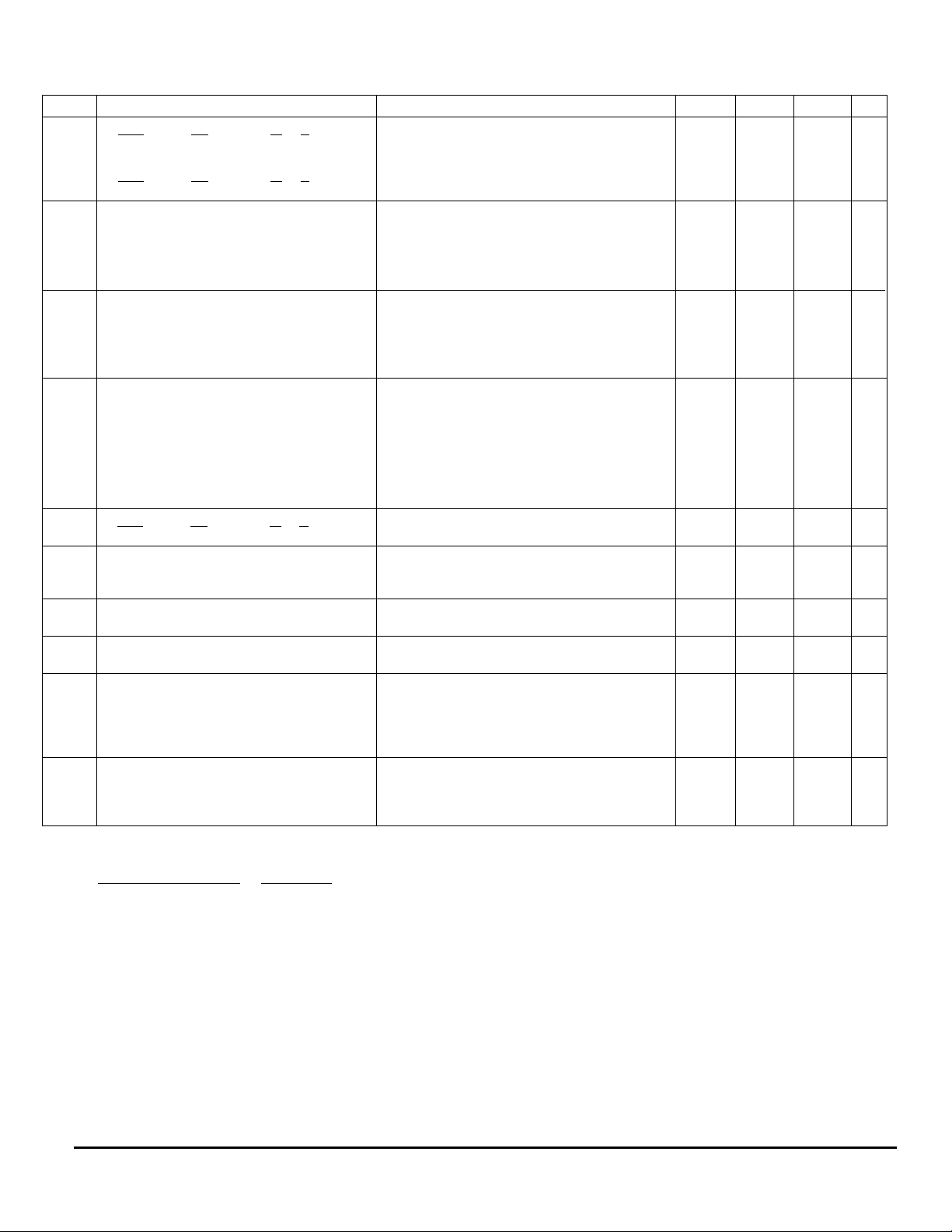
OPERATION OF LIQUID CRYSTAL DISPLAY DRIVER
Description of Block Diagram Module
Command Decoder and Command Interface
This module determines whether the input data is interpreted as
data or command. Data is directed to this module based upon the
input of the D/C pin. If D/C high, data is written to Graphic Display
Data RAM (GDDRAM). D/C low indicates that the input at D0-D7 is
interpreted as a Command.
Reset is of same function as Power ON Reset (POR). Once RES
received the reset pulse, all internal circuitry will back to its initial status. Refer to Command Description section for more information.
Column address 00H
(or column address 77H)
Row 0
Page 1
LSB
MPU Parallel Interface
The parallel interface consists of 8 bi-directional data lines (D0D7), R/W, and the CS. The R/W input High indicates a read operation from the Graphic Display Data RAM (GDDRAM). R/W input Low
indicates a write operation to Display Data RAM or Internal Command Registers depending on the status of D/C input. The CS input
serves as data latch signal (clock). Refer to AC operation conditions
and characteristics section for Parallel Interface Timing Description.
Graphic Display Data RAM (GDDRAM)
The GDDRAM is a bit mapped static RAM holding the bit pattern
to be displayed. The size of the RAM is determined by number of
row times the number of column (120x17 = 2040 bits). Figure 5 is a
description of the GDDRAM address map. For mechanical flexibility,
re-mapping on both Segment and Common outputs are provided.
Column address 77H
(or column address 00H)
Com0
(Com15)
Row 15
Page 3
Page 2
LSBRow 16
MSB
LSB
MSB
Seg0
Note : The configuration in parentheses represent the remapping of Rows and Columns
Figure 5. Graphic Display Data RAM (GDDRAM) Address Map
Com15
(Com0)
Com16
Seg119
MC141531MOTOROLA
3–149

Display Timing Generator
This module is an on chip low power RC oscillator circuitry (Figure 6). The oscillator frequency can be selected in the range of
15kHz to 50kHz by external resistor. One can enable the circuitry by
software command. For external clock provided, feed the clock to
OSC2 and leave OSC1 open.
Annunciator Control Circuit
The LCD waveform of the 3 annunciators and BP are generated
by this module. The 3 independent annunciators are enabled by software command. Annunciator is also controlled by oscillator circuit.
Before turning the annunciators on, the oscillator must be on in
advance. Annunciator output waveform shown in Figure 7.
Internal Oscillator selected
enable1 enable
Oscillation Circuit
OSC1
enable2
OSC2
Buffer
External component
Feedback for internal oscillator
For external CLK input
Figure 6. Oscillator Circuitry
BP
ANNUN1
ANNUN2
ANNUN1 ON / OFF ON ON ON ON ON / OFF
ANNUN2 ON / OFF OFF ON ON OFF ON / OFF
OSC DISABLE ENABLE ENABLE ENABLE ENABLE DISABLE
Oscillator enable
MC141531
DV
DD
DV
SS
DV
DD
DV
SS
DV
DD
DV
SS
Figure 7. Annunciators and BP Display Waveform
LCD Driving Internal DC/DC Converter and Regulator
This module generates the LCD voltage needed for display output. It
takes a single supply input and generate necessary bias voltages. It
consists of :
1. Voltage Doubler and Voltage Tripler
To generate the Vcc voltage. Either Doubler or Tripler can be
enabled.
2. Voltage Regulator
Feedback gain control for initial LCD voltage. It can also be used with
external contrast control.
3. Voltage Divider
Divide the LCD display voltage (V
This is a low power consumption circuit which can save the most dis-
play current compare with traditional resistor ladder method.
4. Self adjust temperature compensation circuitry
Provide 4 different compensation grade selections to satisfy the vari-
ous liquid crystal temperature grades. The grading can be selected
by software control.
5. Contrast Control Block
Software control of 16 voltage levels of LCD voltage.
All blocks can be individually turned off if external DC/DC Converter
is employed.
) from the regulator output.
LL2-VLL6
17 Bit Latch / 120 Bit Latch
A 137 bit long register which carry the display signal information.
First 17 bits are Common driving signals and other 120 bits are Segment driving signals. Data will be input to the HV-buffer Cell for bumping up to the required level.
Level Selector
Level Selector is a control of the display synchronization. Display
voltage can be separated into two sets and used with different cycles.
Synchronization is important since it selects the required LCD voltage
level to the HV Buffer Cell for output signal voltage pump.
HV Buffer Cell (Level Shifter)
HV Buffer Cell works as a level shifter which translates the low voltage output signal to the required driving voltage. The output is shifted
out with an internal FRM clock which comes from the Display Timing
Generator. The voltage levels are given by the level selector which is
synchronized with the internal M signal.
MC141531
3–150
MOTOROLA

LCD Panel Driving Waveform
The following is an example of how the Common and Segment drivers may be connected to a LCD panel. The waveforms shown in Figure
8a, 8b and 8c illustrate the desired multiplex scheme.
COM0
COM1
COM2
COM3
COM4
COM5
COM6
COM7
SEG1
SEG2
SEG3
SEG0
SEG4
Figure 8a. LCD Display Example “0”
MC141531MOTOROLA
3–151

TIME SLOT
COM0
COM1
SEG0
SEG1
1234
Figure 8b. LCD Driving Signal from MC141531
1234
VLL6
VLL5
VLL4
VLL3
VLL2
VLL1
VLL6
VLL5
VLL4
VLL3
VLL2
VLL1
VLL6
VLL5
VLL4
VLL3
VLL2
VLL1
VLL6
VLL5
VLL4
VLL3
VLL2
VLL1
Seg0-Com0
“OFF” Pixel
Seg0-Com1
“On” Pixel
1234
TIME SLOT
1234
VLL6
VLL5
VLL4
VLL3
VLL2
VLL1
-VLL2
-VLL3
-VLL4
-VLL5
-VLL6
VLL6
VLL5
VLL4
VLL3
VLL2
VLL1
-VLL2
-VLL3
-VLL4
-VLL5
-VLL6
MC141531
3–152
Figure 8c. Effective LCD waveform on LCD pixel
MOTOROLA

Command Description
Set Display On/Off (Display Mode / Stand-by Mode)
The Display On command turns the LCD Common and Segment
outputs on and has no effect to the annunciator output. This command starts the conversion of data in GDDRAM to necessary waveforms on the Common and Segment driving outputs. The on-chip
bias generator is also turned on by this command. (Note: “Set Oscillator On” command should be sent before “Set Display On”)
The Display Off command turn the display off and the states of the
LCD driver are as follow during display off:
1. The Common and Segment outputs are fixed at V
2. The bias Internal DC/DC Converter is turned off.
3. The RAM and content of all registers are retained.
4. IC will accept new commands and data.
The status of the Annunciators and Oscillator are not affected by
this command.
Note: DON’T USE ICON DISPLAY MODE DURING DISPLAY
OFF.
Set GDDRAM Column Address
This command positions the address pointer on a column location.
The address can be set to location 00H-77H (120 columns). The column address will be increased automatically after a read or write
operation. Refer to “Address Increment Table” and command “Set
GDDRAM Page Address” for further information.
Set GDDRAM Page Address
This command positions the row address to 1 of 3 possible positions in GDDRAM. Refer to figure 5.
Master Clear GDDRAM
This command is to clear the content of page 1 and 2 of the Display Data RAM to zero. Issue this command followed by a dummy
write command.
LL1
(VSS).
Set Vertical Scroll Value
This command maps the selected GDDRAM row (00H-0FH) to
Com0. With scroll value equals to 0, Row 0 of GDDRAM is mapped
to Com0 and Row 1 through Row 15 are mapped to Com1 through
Com15 respectively. With scroll value equal to 1, Row 1 of
GDDRAM is mapped to Com0, then Row 2 through Row 15 will be
mapped to Com1 through Com14 respectively and Row 0 will be
mapped to Com15.
Save / Restore Column Address
With bit option = 1 in this command, the Save / Restore Column
Address command saves a copy of the Column Address of
GDDRAM. With a bit option = 0, this command restores the copy
obtained from the previous execution of saving column address. This
instruction is very useful for writing full graphics characters that are
larger than 8 pixels vertically.
Set Column Mapping
This instruction selects the mapping of GDDRAM to Segment drivers for mechanical flexibility. There are 2 mappings to select:
1. Column 0 - Column 119 of GDDRAM mapped to Seg0-Seg119
respectively;
2. Column 0 - Column 119 of GDDRAM mapped to Seg119-Seg0
respectively.
Detail information please refer to section “Display Output Description”.
Set Row Mapping
This command selects the mapping of GDDRAM to Common Drivers for mechanical flexibility. There are 2 mappings to select:
1. Row 0 - Row 15 of GDDRAM to Com0 - Com15 respectively;
2. Row 0 - Row 15 of GDDRAM to Com15 - Com0 respectively.
Output of Row 16 (Com16) will not be changed by this command.
See section “Display Output Description” for related information.
Master Clear Icons
This command is used to clear the data in page 3 of GDDRAM
which stores the icon line data. Before using this command, set the
page address to Page 3 by the command “Set GDDRAM Page
Address”. A dummy write data is also needed after this “Master Clear
Icons” command to make the clear icon action effective.
Set Display Mode
This command switch the driver to full display mode or low power
icon mode. In low power icon mode, only icons (driven by COM16)
and annunciators are displayed, and the DC-DC converter, the Internal DC/DC Converter and the regulator are disabled. Do select 1/17
Mux ratio before using the low power icon mode.
Note: DON’T USE ICON DISPLAY MODE DURING DISPLAY OFF.
Set Multiplex Ratio
In normal display mode, the multiplex ratio could be set to be 1/16
or 1/17. For 1/16 Mux Ratio, COM16 signal should not be connected
to the panel.
Set Icon Mode A/B
In Icon mode A, on-pixels are stressed by a voltage with rootmean-square value of 0.87xVDD, whereas off-pixels by 0.5xVDD. In
icon mode B, on-pixels are stressed by a voltage with root-meansquare value of 0.71xVDD, whereas off-pixels by 0.41xVDD. This
command is used to control the contrast of the icon line (Com16)
under icon mode
Set Annunciator Control Signals
This command is used to control the active states of the 3 stand
alone annunciator drivers.
Set Oscillator Enable / Disable
This command is used to either turn on or off the oscillator. For
using internal or external oscillator, this command should be executed. The setting for this command is not affected by command “Set
Display On/Off” and “Set Annunciator Control Signal”. See command
“Set Internal / External Oscillator” for more information
Set Internal / External Oscillator
This command is used to select either internal or external oscillator. When internal oscillator is selected, feedback resistor between
OSC1 and OSC2 is needed. For external oscillation circuit, feed
clock input signal to OSC2 and leave OSC1 open.
Set Internal DC/DC Converter On/Off
Use this command to select the Internal DC/DC Converter to generate the VCC from AVDD. Disable the Internal DC/DC Converter if
external Vcc is provided.
Set Voltage Doubler / Tripler
Use this command to choose Doubler or Tripler when the Internal
DC/DC Converter is enabled.
MC141531MOTOROLA
3–153

Set Internal Regulator On/Off
Choose bit option 0 to disable the Internal Regulator. Choose bit
option 1 to enable Internal Regulator which consists of the internal
contrast control and temperature compensation circuits.
Increase / Decrease Contrast Level
If the internal contrast control is enabled, this command is used to
increase or decrease the contrast level within the 16 contrast levels.
The contrast level starts from lowest value after POR.
Set Internal Voltage Divider On/Off
If the Internal Voltage Divider is disabled, external bias can be
used for V
LL6
to V
If the Internal Voltage Divider is enabled, the
LL2.
internal circuit will generated the 1:5 bias driving voltage.
Set Internal Contrast Control On/Off
This command is used to turn on or off the internal control of delta
voltage of the bias voltages. With bit option = 1, the software selection for delta bias voltage control is enabled. With bit option = 0, internal contrast control is disabled.
Set Contrast Level
This command is to select one of the 16 contrast levels when internal contrast control circuitry is in use. After power-on reset, the contrast level is the lowest.
Set Temperature Coefficient
This command can select 4 different LCD driving voltage temperature coefficients to match various liquid crystal temperature grades.
Those temperature coefficients are specified in Electrical Characteristics Tables.
COMMAND TABLE
Bit Pattern Command Comment
000000X1X
0001X3X2X1X
0010000X
0010001X
0010010X
0010100X
0010101X
0010110X
0010111X
0011000X
0011001X
0011010X
0
0
0
0
0
0
0
0
0
0
0
0
00110110 Master Clear GDDRAM Master clear page 1 and 2 of GDDRAM
00110111 Master Clear of Icons Master Clear of icon line (Com16)
0011101X
0
Set GDDRAM Page Address Set GDDRAM Page Address using X1X0 as address bits.
X1X0=00 : page 1 (POR)
X1X0=01 : page 2
X1X0=10 : page 3
Set Contrast Level With R/W pin input low, set one of the 16 available values to the
internal contrast register, using X3X2X1X0 as data bits. The contrast register is reset to 0000 during POR.
Set Voltage Doubler / Tripler X0=0 : Set Voltage Tripler (POR)
X0=1 : Set Voltage Doubler
Set Column Mapping X0=0 : Col0 to Seg0 (POR)
X0=1 : Col0 to Seg119
Set Row Mapping X0=0 : Row0 to Com0
X0=1 : Row0 to Com15
Set Display On/Off X0=0 : display off (POR)
X0=1 : display on
Set Internal DC/DC Converter On/Off X0=0 : Internal DC/DC Converter off(POR)
X0=1 : Internal DC/DC Converter on
Set Internal Regulator On/Off X0=0 : Internal Regulator off(POR)
X0=1 : Internal Regulator on
When application uses a supply with built-in temperature compensation, the regulator should be disabled.
Set Internal Voltage Divider On/Off X0=0 : Internal Voltage Divider off (POR)
X0=1 : Internal Voltage Divider on
When an external bias network is preferred, the voltage divider
should be disabled.
Set Internal Contrast Control On/Off X0=0 : Internal Contrast Control off (POR)
X0=1 : Internal Contrast Control on
Internal contrast circuits can be disabled if external contrast circuits is preferred.
Set Display Mode X0=0 : normal display mode (1/16 or 1/17 mux) (POR)
X0=1 : low power icon display mode
Save/Restore GDDRAM Column
Address
X0=0 : restore address
X0=1 : save address
Reserved. X0=0: normal operation (POR)
X0=1: test mode
(Note: Make sure to set X0=0 during application)
MC141531
3–154
MOTOROLA

Bit Pattern Command Comment
0011110X
0
Set Multiplex Ratio X0=0 : 1/16 Mux ratio (POR)
X0=1 : 1/17 Mux ratio
0011111X
0
Set Icon Mode A/B X0=0 : icon mode A (POR)
X0=1 : icon mode B
0100X3X2X1X
0
Set Vertical Scroll Value Use X3X2X1X0 as number of lines to scroll.
Scroll value = 0 upon POR
01100A1A0X
0
Set Annunciator Control Signals A1A0=00 : select annunciator 1 (POR)
A1A0=01 : select annunciator 2
A1A0=10 : select annunciator 3
X0=0 : turn selected annunciator off (POR)
X0=1 : turn selected annunciator on
01101000 Reserved
011011X1X
0
Set Temperature Coefficient X1X0= 00 : 0.00% (POR)
X1X0= 01 : -0.18%
X1X0= 10 : -0.22%
X1X0= 11 : -0.35%
0111000X
0
Increase / Decrease Contrast Value X0=0 : Decrease by one
X0=1 : Increase by one
(Note: increment/decrement wraps round among the 16 contrast
levels. Start at the lowest level when POR.)
0111011X
0
Reserved X0=0: normal operation (POR)
X0=1: test mode select
(Note: Make sure to set X0=0 during application)
0111101X
0
Set External / Internal Oscillator X0=0: External oscillator (POR)
X0=1: Internal oscillator.
For internal oscillator place a resistor between OSC1 and OSC2.
For external oscillator mode, feed clock input to OSC2.
0111111X
0
Set Oscillator Disable / Enable X0=0: oscillator master disable (POR)
X0=1: oscillator master enable.
This is the master control for oscillator circuitry. This command
should be issued after the “External / Internal Oscillator” com-
mand.
1X6X5X4X3X2X1X
0
Set GDDRAM Column Address Set GDDRAM Column Address.
Use X6X5X4X3X2X1X0 as address bits.
Data Read / Write
To read data from the GDDRAM, input High to R/W pin and D/C pin. Data is valid at the falling edge of CS. And the GDDRAM column
address pointer will be increased by one automatically.
To write data to the GDDRAM, input Low to R/W pin and High to D/C pin. Data is latched at the falling edge of CS. And the GDDRAM column
address pointer will be increased by one automatically.
No auto address pointer increment will be performed for the Dummy Write Data after Master Clear GDDRAM. (Refer to the “Commands
Required for R/W Actions on RAM” Table)
MC141531MOTOROLA
3–155

Address Increment Table (Automatic)
D/CR/W Comment Address Increment Remarks
0 0 Write Command No
0 1 Read Command No (invalid mode) *1
1 0 Write Data Yes *2
1 1 Read Data Yes
Address Increment is done automatically data read write. The column address pointer of GDDRAM*3 is affected.
Remarks : *1. Only data is read from RAM.
*2. If write data is issued after Command Clear RAM, Address increase is not applied.
*3. Column Address will be wrapped round when overflow.
Power Up Sequence (Commands Required)
Command Required POR Status Remarks
Set External / Internal Oscillator
Set Voltage Tripler / Doubler
Internal DC/DC Converter On
Set Internal Regulator On
Set Temperature Coefficient
Set Internal Contrast On
Set Contrast Level
Set Internal Voltage Divider On
Set Column Mapping
Set Row Mapping
Set Vertical Scroll Value
Set Oscillator Enable
Set Annunciator Control Signals
Master Clear GDDRAM
Dummy Write Data
Set Display On
External
Tripler
Off
Off
TC=0%
Off
Contrast Level = 0
Off
Seg. 0 = Col. 0
Com. 0 = Row 0
Scroll Value = 0
Disable
Annunciators all off
Random
Off
*1
*1
*1
*1
*1, *3
*1, *3
*1, *2, *3
*1
*1
*1
*1
*1
Remarks :
*1 -- Required only if desired status differ from POR.
*2 -- Effective only if Internal Contrast Control is enabled.
*3 -- Effective only if Regulator is enabled.
MC141531
3–156
MOTOROLA

Commands Required for Display Mode Setup
Display Mode Commands Required
Normal Display Mode Set External / Internal Oscillator
Set Oscillator Enable,
Set Display On.
Icon Display Mode Set Internal Oscillator
Set Oscillator Enable,
Set Display Mode to Icon Display Mode
Set Display On.
Annunciator Display Set External / Internal Oscillator
Set Oscillator Enable,
Set Annunciator On/Off.
Standby Mode Set Display Off,
Set Oscillator Disable.
Other Related Command with Display Mode: Set Column Mapping, Set Row Mapping, Set Vertical Scroll Value.
Commands Related to Internal DC/DC Converter:
Set Oscillator Disable / Enable, Set Internal Regulator On/Off, Set Temperature Coefficient, Set Internal Contrast Control On/Off, Increase /
Decrease Contrast Level, Set Internal Voltage Divider On/Off, Set Display On/Off, Set Internal / External Oscillator, Set Contrast Level, Set
Voltage Doubler / Tripler
* No need to resend the command again if it is set previously.
(0111101X0)*
(01111111)*
(00101001)*
(01111011)*
(01111111)*
(00110011)*
(00101001)*
(0111101X0)*
(01111111)*
(01100A1A0X0)*
(00101000)*
(01111110)*
Commands Required for R/W Actions on RAM
R/W Actions on RAMs Commands Required
Read/Write Data from/to GDDRAM. Set GDDRAM Page Address
Set GDDRAM Column Address
Read/Write Data
Save/Restore GDDRAM Column Address. Save/Restore GDDRAM Column Address. (0011010X0)
Increase GDDRAM Column Address by One Dummy Read Data (X7X6X5X4X3X2X1X0)
Master Clear GDDRAM Master Clear GDDRAM
Dummy Write Data
* No need to resend the command again if it is set previously.
The read / write action to the Display Data RAM does not depend on the display mode. This means the user can change the RAM content
whether the target RAM content is being displayed.
(000000X1X0)*
(1X6X5X4X3X2X1X0)*
(X7X6X5X4X3X2X1X0)
(00110110)
(X7X6X5X4X3X2X1X0)
MC141531MOTOROLA
3–157

Display Output Description
This is an example of output pattern on the LCD panel. The following
table is a description of what is inside the CDDRAM, CGRAM and GDDRAM. Figure 9b and 9c are the output pattern on the LCD display with
different command enabled.
(Display Mode, Page Swapping, Scrolling, Column Re-map and Row
Re-map)
COM0
COM16
SEG0 SEG119
Figure 9a
Content of GDDRAM
PAGE 1 5A5A5A5A-----------------00000000
5A5A5A5A-----------------00000000
PAGE 2 33CC33CC-----------------33CC33CC
33CC33CC-----------------33CC33CC
Figure 9b
Column remap disable
Row re-map disable
Column remap enable
Row re-map disable
Column remap disable
Row re-map enable
Figure 9c. Examples of LCD display with different command enabled
Column remap disable
Row re-map disable
Scroll Value = 0Fh
MC141531
3–158
MOTOROLA

PACKAGE DIMENSIONS
MC141531T
TAB PACKAGE DIMENSION - 1
98ASL00247A ISSUE0
COPPER SIDE
MC141531MOTOROLA
3–159

PACKAGE DIMENSIONS
MC141531T
TAB PACKAGE DIMENSION - 2
98ASL00247A ISSUE0
MC141531
3–160
MOTOROLA

Application Circuit
16/17 MUX Display with Analog Circuitry enabled, Tripler enabled and 1:5 bias
CMOS
MPU/
MCU with
Parallel
Interface
EPROM
DV
0.1µF
DVSS DVDD
RES
D/C
CS
R/W
D0~D7
RAM
DD
AV
DD
AVDD
0.1µF
AVSS
0.1µF 0.1µF 0.1µF 0.1µF 0.1µF 0.1µF
VLL2 VLL3 VLL4 VLL5 VLL6 VCC
MC141531
OSC2 OSC1 C+ C- VF VR C2P C2N C1P C1N
760kΩ
1MΩ
560pF
200kΩ
0.1µF 0.1µF0.1µF
4.7µF
COM0 to
COM16
SEG0 to
SEG119
Annun 0-2
and BP
To LCD
Panel
Remark :
1. Capacitor between C2N and C2P can be omitted only if doubler is enable.
2. Resistor across OSC1 and OSC2 can be omitted if external oscillator is used.
3. VR and VF can be left open for Regulator disable, TC = 0% and Contrast Disable.
4. RES, CS, R/W and D/C should be at a known state.
5. CS line low at Standby Mode.
MC141531MOTOROLA
3–161

Application Circuit
16/17 MUX Display with Analog Circuit disabled, External Bias
CMOS
MPU/
MCU with
Parallel
Interface
EPROM
DV
0.1µF
DVSS DVDD
RES
D/C
CS
R/W
D0~D7
RAM
DD
AV
DD
0.1µF
AVDD
OSC2
External Clock
VLL2 VLL3 VLL4 VLL5 VLL6 VCCAVSS
MC141531
OSC1 C+ C- VF VR C2P C2N
V
CC
COM0 to
COM16
SEG0 to
SEG119
Annun 0-2
and BP
C1N
C1P
To LCD
Panel
MC141531
3–162
Remark :
1. Value of the resistors depends on the LCD panel characteristic.
2. RES, CS, R/W and D/C should be at a known state.
3. CS line low at Standby Mode.
MOTOROLA

Die Pad Coordinate of MC141531
Pad Pin Name X (um) Y(um)
1 OSC2 -3685 -762.9 76x76 71 SEG102 3925 631.5 50x108 141 SEG32 -1409 631.5 50x108
2 AVSS -3487 -762.9 76x76 72 SEG101 3849 631.5 50x108 142 SEG31 -1485 631.5 50x108
3 VR -3290 -762.9 76x76 73 SEG100 3773 631.5 50x108 143 SEG30 -1561 631.5 50x108
4 VF -3183 -762.9 76x76 74 SEG99 3697 631.5 50x108 144 SEG29 -1637 631.5 50x108
5 VCC -2985 -762.9 76x76 75 SEG98 3620 631.5 50x108 145 SEG28 -1714 631.5 50x108
6 C- -2787 -762.9 76x76 76 SEG97 3544 631.5 50x108 146 SEG27 -1790 631.5 50x108
7 C+ -2590 -762.9 76x76 77 SEG96 3468 631.5 50x108 147 SEG26 -1866 631.5 50x108
8 VLL6 -2392 -762.9 76x76 78 SEG95 3392 631.5 50x108 148 SEG25 -1942 631.5 50x108
9 VLL5 -2194 -762.9 76x76 79 SEG94 3316 631.5 50x108 149 SEG24 -2018 631.5 50x108
10 VLL4 -1997 -762.9 76x76 80 SEG93 3239 631.5 50x108 150 SEG23 -2095 631.5 50x108
11 OSC1 -1789 -762.9 76x76 81 SEG92 3163 631.5 50x108 151 SEG22 -2171 631.5 50x108
12 VLL3 -1682 -762.9 76x76 82 SEG91 3087 631.5 50x108 152 SEG21 -2247 631.5 50x108
13 VLL2 -1485 -763.2 76x76 83 SEG90 3011 631.5 50x108 153 SEG20 -2323 631.5 50x108
14 C1N -1287 -762.9 76x76 84 SEG89 2935 631.5 50x108 154 SEG19 -2399 631.5 50x108
15 C1P -1089 -762.9 76x76 85 SEG88 2858 631.5 50x108 155 SEG18 -2476 631.5 50x108
16 C2N -891.6 -762.9 76x76 86 SEG87 2782 631.5 50x108 156 SEG17 -2552 631.5 50x108
17 C2P -693.9 -762.9 76x76 87 SEG86 2706 631.5 50x108 157 SEG16 -2628 631.5 50x108
18 AVDD -496.2 -762.9 76x76 88 SEG85 2630 631.5 50x108 158 SEG15 -2704 631.5 50x108
19 AVDD -298.5 -762.9 76x76 89 SEG84 2554 631.5 50x108 159 SEG14 -2780 631.5 50x108
20 DVSS -99 -762.9 76x76 90 SEG83 2477 631.5 50x108 160 SEG13 -2857 631.5 50x108
21 DVSS 18 -762.9 76x76 91 SEG82 2401 631.5 50x108 161 SEG12 -2933 631.5 50x108
22 DVSS 124.8 -762.9 76x76 92 SEG81 2325 631.5 50x108 162 SEG11 -3009 631.5 50x108
23 D7 241.8 -762.9 76x76 93 SEG80 2249 631.5 50x108 163 SEG10 -3085 631.5 50x108
24 DVSS 348.6 -762.9 76x76 94 SEG79 2173 631.5 50x108 164 SEG9 -3161 631.5 50x108
25 D6 465.6 -762.9 76x76 95 SEG78 2096 631.5 50x108 165 SEG8 -3238 631.5 50x108
26 DVSS 572.4 -762.9 76x76 96 SEG77 2020 631.5 50x108 166 SEG7 -3314 631.5 50x108
27 D5 689.4 -762.9 76x76 97 SEG76 1944 631.5 50x108 167 SEG6 -3390 631.5 50x108
28 DVSS 796.2 -762.9 76x76 98 SEG75 1868 631.5 50x108 168 SEG5 -3466 631.5 50x108
29 D4 913.2 -762.9 76x76 99 SEG74 1792 631.5 50x108 169 SEG4 -3542 631.5 50x108
30 DVSS 1020 -762.9 76x76 100 SEG73 1715 631.5 50x108 170 SEG3 -3619 631.5 50x108
31 D3 1137 -762.9 76x76 101 SEG72 1639 631.5 50x108 171 SEG2 -3695 631.5 50x108
32 DVSS 1244 -762.9 76x76 102 SEG71 1563 631.5 50x108 172 SEG1 -3771 631.5 50x108
33 D2 1361 -762.9 76x76 103 SEG70 1487 631.5 50x108 173 SEG0 -3847 631.5 50x108
34 DVSS 1468 -762.9 76x76 104 SEG69 1411 631.5 50x108 174 COM16 -3930 631.5 50x108
35 D1 1585 -762.9 76x76 105 SEG68 1334 631.5 50x108 175 COM15 -4006 631.5 50x108
36 DVSS 1691 -762.9 76x76 106 SEG67 1258 631.5 50x108 176 COM14 -4082 631.5 50x108
37 D0 1808 -762.9 76x76 107 SEG66 1182 631.5 50x108 177 COM13 -4159 631.5 50x108
38 DVSS 1915 -762.9 76x76 108 SEG65 1106 631.5 50x108 178 COM12 -4235 631.5 50x108
CS 2032 -762.9 76x76 109 SEG64 1030 631.5 50x108 179 COM11 -4311 631.5 50x108
39
40 DVSS 2139 -762.9 76x76 110 SEG63 953.4 631.5 50x108 180 COM10 -4254 140.1 108x50
41 R/W 2256 -762.9 76x76 111 SEG62 877.2 631.5 50x108 181 COM9 -4254 63.9 108x50
42 DVSS 2363 -762.9 76x76 112 SEG61 801 631.5 50x108 182 COM8 -4254 -12.3 108x50
43 D/C 2480 -762.9 76x76 113 SEG60 724.8 631.5 50x108 183 COM7 -4254 -88.5 108x50
44 RES 2587 -762.9 76x76 114 SEG59 648.6 631.5 50x108 184 COM6 -4254 -164.7 108x50
45 DVDD 2794 -762.9 76x76 115 SEG58 572.4 631.5 50x108 185 COM5 -4254 -240.9 108x50
46 BP 2901 -762.9 76x76 116 SEG57 496.2 631.5 50x108 186 COM4 -4254 -317.1 108x50
47 DVSS 3018 -762.9 76x76 117 SEG56 420 631.5 50x108 187 COM3 -4254 -393.3 108x50
48 ANNUN2 3125 -762.9 76x76 118 SEG55 343.8 631.5 50x108 188 COM2 -4254 -469.5 108x50
49 DVSS 3242 -762.9 76x76 119 SEG54 267.6 631.5 50x108 189 COM1 -4254 -545.7 108x50
50 ANNUN1 3348 -762.9 76x76 120 SEG53 191.4 631.5 50x108 190 COM0 -4254 -621.9 108x50
51 DVSS 3465 -762.9 76x76 121 SEG52 115.2 631.5 50x108 191 COM16 -4254 -698.1 108x50
52 ANNUN0 3572 -762.9 76x76 122 SEG51 39 631.5 50x108
53 DVSS 3689 -762.9 76x76 123 SEG50 -37.2 631.5 50x108
54 SEG119 4254 -697.2 108x50 124 SEG49 -113.4 631.5 50x108
55 SEG118 4254 -621 108x50 125 SEG48 -189.6 631.5 50x108
56 SEG117 4254 -544.8 108x50 126 SEG47 -265.8 631.5 50x108
57 SEG116 4254 -468.6 108x50 127 SEG46 -342 631.5 50x108
58 SEG115 4254 -392.4 108x50 128 SEG45 -418.2 631.5 50x108
59 SEG114 4254 -316.2 108x50 129 SEG44 -494.4 631.5 50x108
60 SEG113 4254 -240 108x50 130 SEG43 -570.6 631.5 50x108
61 SEG112 4254 -163.8 108x50 131 SEG42 -646.8 631.5 50x108
62 SEG111 4254 -87.6 108x50 132 SEG41 -723 631.5 50x108
63 SEG110 4254 -11.4 108x50 133 SEG40 -799.2 631.5 50x108
64 SEG109 4254 64.8 108x50 134 SEG39 -875.4 631.5 50x108
65 SEG108 4254 141 108x50 135 SEG38 -951.6 631.5 50x108
66 SEG107 4306 631.5 50x108 136 SEG37 -1028 631.5 50x108
67 SEG106 4230 631.5 50x108 137 SEG36 -1104 631.5 50x108
68 SEG105 4154 631.5 50x108 138 SEG35 -1180 631.5 50x108
69 SEG104 4078 631.5 50x108 139 SEG34 -1256 631.5 50x108
70 SEG103 4001 631.5 50x108 140 SEG33 -1333 631.5 50x108
Bump
Pad Pin Name X (um) Y(um)
Size (um)
Bump
Pad Pin Name X (um) Y(um)
Size (um)
Bump
Size (um)
Die Size : 358.5 X 78 mil
MC141531MOTOROLA
3–163
 Loading...