

Motorola MC141518, MC141518FJ Datasheet
MCM63P736•MCM63P818
1
MOTOROLA FAST SRAM
Product Preview
128K x 36 and 256K x 18 Bit
Pipelined BurstRAM
Synchronous Fast Static RAM
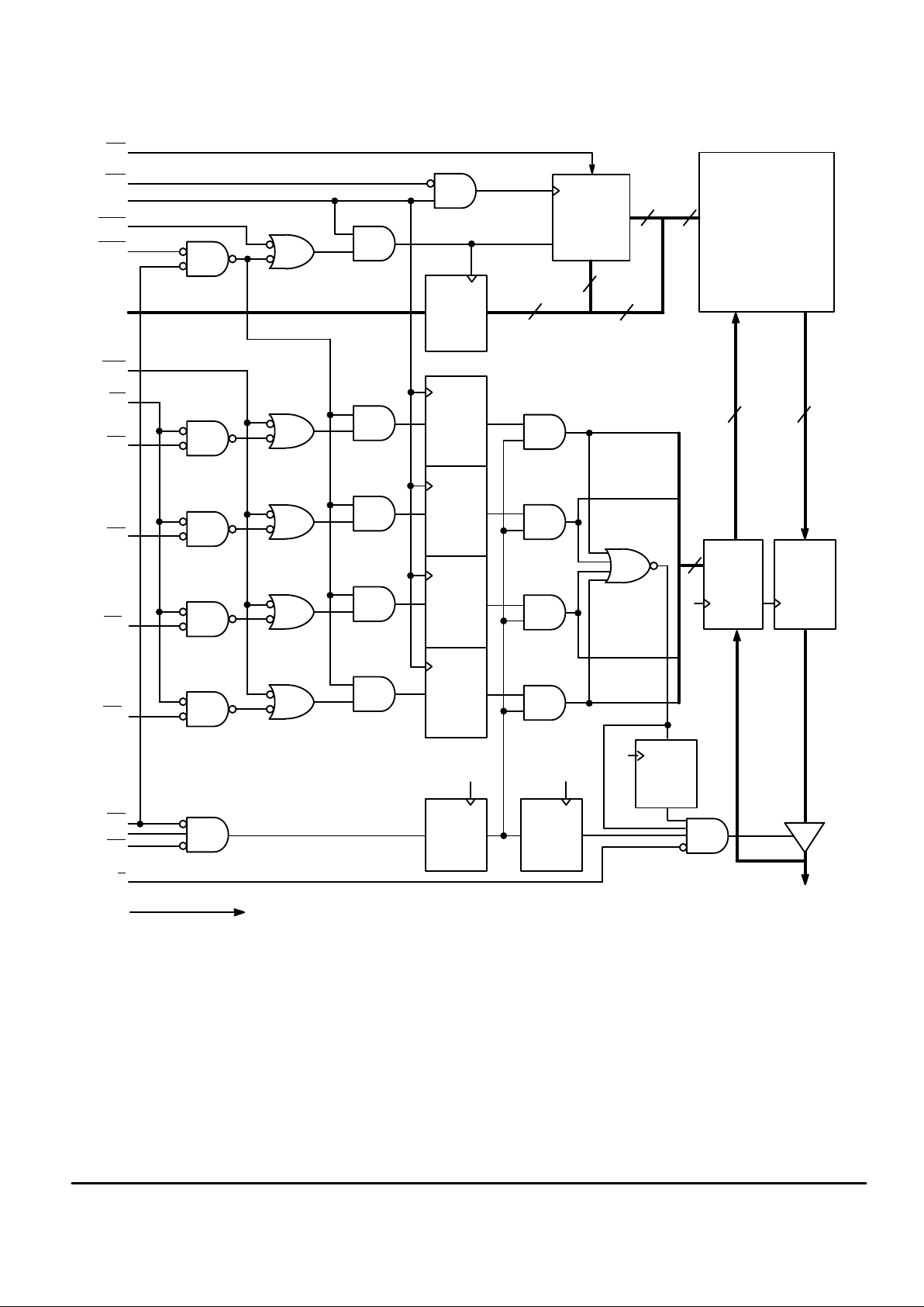
The MCM63P736 and MCM63P818 are 4M bit synchronous fast static RAMs
designed to provide a burstable, high performance, secondary cache for the
PowerPC and other high performance microprocessors. The MCM63P736 is
organized as 128K words of 36 bits each and the MCM63P818 is organized as
256K words of 18 bits each. These devices integrate input registers, an output
register, a 2–bit address counter , and high speed SRAM onto a single monolithic
circuit for reduced parts count in cache data RAM applications. Synchronous design allows precise cycle control with the use of an external clock (K).
Addresses (SA), data inputs (DQx), and all control signals except output
enable (G
), sleep mode (ZZ), and linear burst order (LBO) are clock (K) controlled
through positive–edge–triggered noninverting registers.
Bursts can be initiated with either ADSP
or ADSC input pins. Subsequent burst
addresses can be generated internally by the MCM63P736 and MCM63P818
(burst sequence operates in linear or interleaved mode dependent upon the state
of LBO
) and controlled by the burst address advance (ADV) input pin.
Write cycles are internally self–timed and are initiated by the rising edge of the
clock (K) input. This feature eliminates complex off–chip write pulse generation
and provides increased timing flexibility for incoming signals.
Synchronous byte write (SBx
), synchronous global write (SGW), and synchro-
nous write enable (SW
) are provided to allow writes to either individual bytes or
to all bytes. The bytes are designated as “a”, “b”, etc. SBa
controls DQa, SBb con-
trols DQb, etc. Individual bytes are written if the selected byte writes SBx
are asserted with SW. All bytes are written if either SGW is asserted or if all SBx and
SW
are asserted.
For read cycles, pipelined SRAMs output data is temporarily stored by an
edge–triggered output register and then released to the output buffers at the next
rising edge of clock (K).
The MCM63P736 and MCM63P818 operate from a 3.3 V core power supply
and all outputs operate on a 2.5 V or 3.3 V power supply. All inputs and outputs
are JEDEC standard JESD8–5 compatible.
• MCM63P736/MCM63P818–133 = 4 ns Access/7.5 ns Cycle (133 MHz)
MCM63P736/MCM63P818–100 = 5 ns Access/10 ns Cycle (100 MHz)
MCM63P736/MCM63P818–66 = 7 ns Access/15 ns Cycle (66 MHz)
• 3.3 V + 10%, – 5% Core Power Supply, 2.5 V or 3.3 V I/O Supply
• ADSP
, ADSC, and ADV Burst Control Pins
• Selectable Burst Sequencing Order (Linear/Interleaved)
• Two–Cycle Deselect Timing
• Internally Self–Timed Write Cycle
• Byte Write and Global Write Control
• Sleep Mode (ZZ)
• PB1 Version 2.0 Compatible
• JEDEC Standard 119–Pin PBGA and 100–Pin TQFP Packages
The PowerPC name is a trademark of IBM Corp., used under license therefrom.
This document contains information on a product under development. Motorola reserves the right to change or discontinue this product without notice.
Order this document
by MCM63P736/D
MOTOROLA
SEMICONDUCTOR TECHNICAL DATA
MCM63P736
MCM63P818
ZP PACKAGE
PBGA
CASE 999–01
TQ PACKAGE
TQFP
CASE 983A–01
10/8/97
Motorola, Inc. 1997
MCM63P736•MCM63P818
2
MOTOROLA FAST SRAM
WRITE
REGISTER
a
WRITE
REGISTER
b
ENABLE
REGISTER
BURST
COUNTER
ADSP
G
CLR
WRITE
REGISTER
c*
WRITE
REGISTER
d*
SBa
SBb
SBc*
SBd*
SE3
15/16
17/18
SGW
DATA–OUT
REGISTER
ENABLE
REGISTER
K2 K
ADDRESS
REGISTER
17/18
DATA–IN
REGISTER
128K x 36 /
256K x 18
ARRAY
SE2
LBO
ADV
K
ADSC
SA
SA1
SA0
SW
SE1
K
4/2
36/18
2
2
K2
DQa – DQd /
DQa – DQb
36/18
FUNCTIONAL BLOCK DIAGRAM
WRITE
REGISTER
K
ZZ
*Valid only for MCM63P736.
MCM63P736•MCM63P818
3
MOTOROLA FAST SRAM
6543217
B
C
V
SS
G
A
D
E
F
H
J
V
SS
V
SS
SBb
V
SS
SA
V
SS
V
SS
V
SS
SA SA SA SA
SA SA SA SA
NC SA SA NC
NC
NC
DQb
SA SA
NC
ZZ
SW
DQa
DQa
V
DDQ
V
DDQ
DQb
V
DDQ
DQb
DQb
DQa
DQa
NCV
DD
NC
SA
NCNC
NC
NC
DQd DQd VSSSA0
NC
LBO
DQa
DQaSA1V
SS
DQdDQd
V
DDQ
DQd V
SS
NC
DQa
DQaSBa
SBdDQdDQd
DQd DQd V
SS
KV
SS
DQc
DQa
V
DD
NCV
DD
NCV
DD
V
DDQ
DQc VSSSGW
DQb
DQb
DQbADV
SBcDQcDQc
V
DDQ
DQc V
SS
G
DQbSE1V
SS
DQcDQc
DQc DQc VSSNC DQb
V
DD
NC
NC SE2 SA ADSC
ADSP
K
L
M
N
P
R
T
U
V
DDQ
V
DDQ
SE3
V
DDQ
V
DDQ
NC
71
72
DQc
V
DDQ
DQb
69
70
66
67
68
64
65
61
62
63
3738343536 42433940 41 454644
60
59
58
57
56
55
54
53
52
51
31 3233
74
75
76
77
78
79
80
50494847
DQb
DQb
V
SS
DQb
DQb
DQb
DQb
V
SS
V
DDQ
DQb
DQb
V
DDQ
V
SS
V
SS
V
DDQ
DQc
DQc
DQc
DQc
DQc
DQc
DQc
NC
SASASE1
SBd
K
SBc
ADV
G
SA0
SASASA
SA
NC
NC
NC
LBO
SA1
V
DD
V
DD
NC
DQa
V
SS
DQa
DQa
DQa
DQa
V
SS
V
DDQ
DQa
DQa
V
SS
V
DDQ
DQa
DQa
DQd
V
DD
V
SS
V
SS
V
DDQ
DQd
DQd
DQd
DQd
DQd
73
DQc
94 93979695 89889291 90 86858710099 98 81828384
10
9
12
11
15
14
13
17
16
20
19
18
21
22
23
24
25
26
27
28
29
30
7
6
5
4
3
2
1
8
SA
SA
SW
SE2
SE3
VSSV
DD
ZZ
NC
V
DDQ
V
SS
DQd
DQd
DQd
SA
SA
SASASA
SA
SA
NC
V
SS
ADSP
ADSC
SGW
SBa
SBb
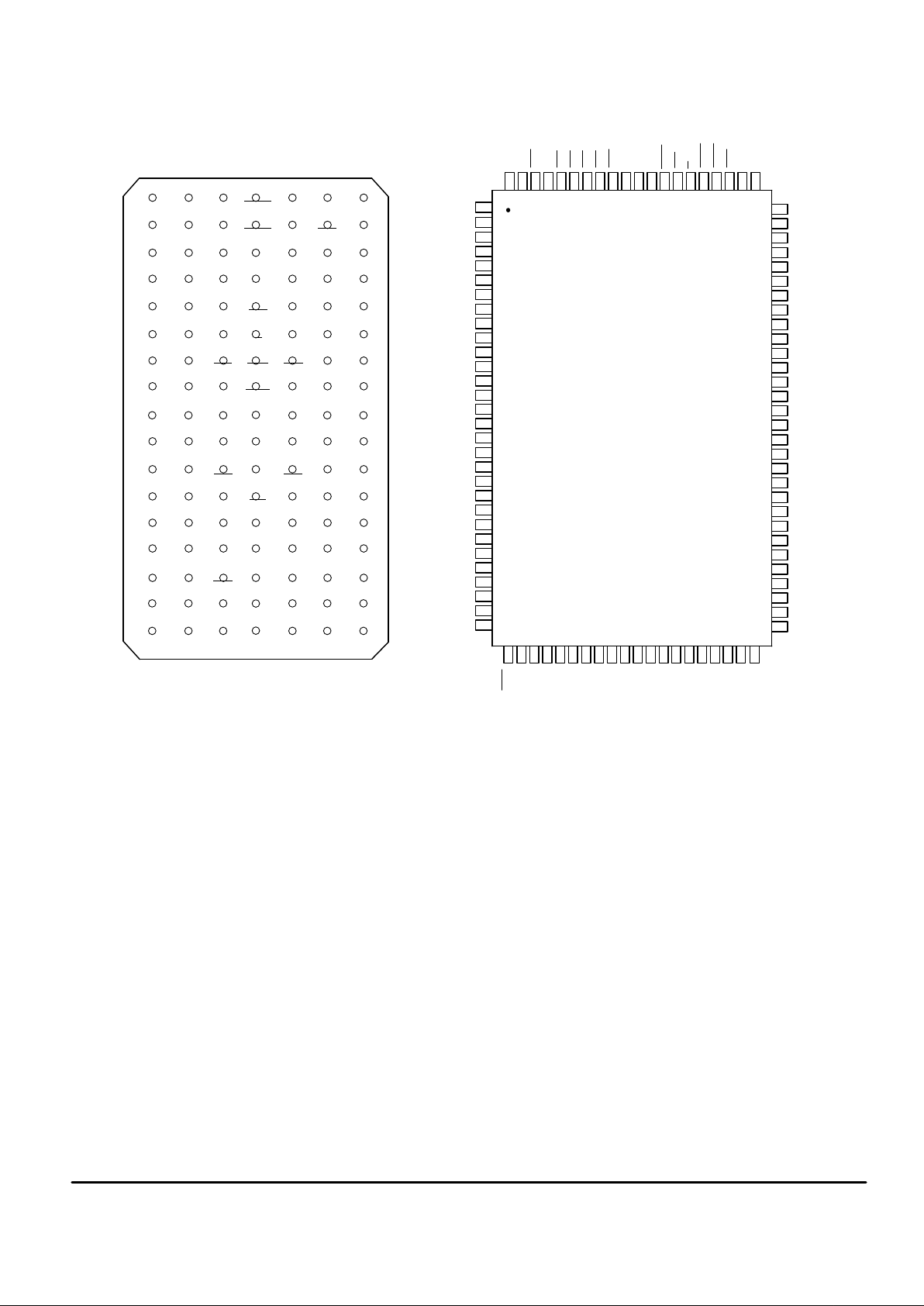
TOP VIEW 119 BUMP PBGA
Not to Scale
TOP VIEW 100 PIN TQFP
MCM63P736 PIN ASSIGNMENTS
MCM63P736•MCM63P818
4
MOTOROLA FAST SRAM
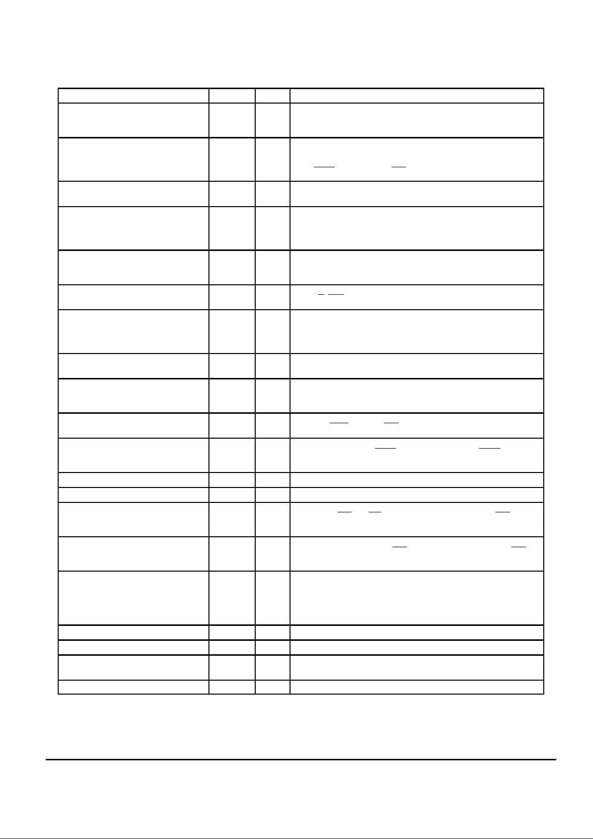
MCM63P736 PBGA PIN DESCRIPTIONS
Pin Locations Symbol
Type Description
4B ADSC Input Synchronous Address Status Controller: Active low, interrupts any
ongoing burst and latches a new external address. Used to initiate a
READ, WRITE, or chip deselect.
4A ADSP Input Synchronous Address Status Processor: Active low, interrupts any
ongoing burst and latches a new external address. Used to initiate a
new READ or chip deselect (exception — chip deselect does not occur
when ADSP
is asserted and SE1 is high).
4G ADV Input Synchronous Address Advance: Increments address count in
accordance with counter type selected (linear/interleaved).
(a) 6K, 7K, 6L, 7L, 6M, 6N, 7N, 6P, 7P
(b) 6D, 7D, 6E, 7E, 6F, 6G, 7G, 6H, 7H
(c) 1D, 2D, 1E, 2E, 2F, 1G, 2G, 1H, 2H
(d) 1K, 2K, 1L, 2L, 2M, 1N, 2N, 1P, 2P
DQx I/O Synchronous Data I/O: “x” refers to the byte being read or written
(byte a, b, c, d).
4F G Input Asynchronous Output Enable Input:
Low — enables output buffers (DQx pins).
High — DQx pins are high impedance.
4K K Input Clock: This signal registers the address, data in, and all control signals
except G
, LBO, and ZZ.
3R LBO Input Linear Burst Order Input: This pin must remain in steady state (this
signal not registered or latched). It must be tied high or low.
Low — linear burst counter (68K/PowerPC).
High — interleaved burst counter (486/i960/Pentium).
2A, 3A, 5A, 6A, 3B, 5B, 2C, 3C,
5C, 6C, 2R, 6R, 3T, 4T, 5T
SA Input Synchronous Address Inputs: These inputs are registered and must
meet setup and hold times.
4N, 4P SA1, SA0 Input Synchronous Address Inputs: These pins must be wired to the two
LSBs of the address bus for proper burst operation. These inputs are
registered and must meet setup and hold times.
5L, 5G, 3G, 3L
(a) (b) (c) (d)
SBx Input Synchronous Byte Write Inputs: “x” refers to the byte being written (byte
a, b, c, d). SGW
overrides SBx.
4E SE1 Input Synchronous Chip Enable: Active low to enable chip.
Negated high — blocks ADSP
or deselects chip when ADSC is
asserted.
2B SE2 Input Synchronous Chip Enable: Active high for depth expansion.
6B SE3 Input Synchronous Chip Enable: Active low for depth expansion.
4H SGW Input Synchronous Global Write: This signal writes all bytes regardless of the
status of the SBx
and SW signals. If only byte write signals SBx are
being used, tie this pin high.
4M SW Input Synchronous Write: This signal writes only those bytes that have been
selected using the byte write SBx
pins. If only byte write signals SBx
are being used, tie this pin low.
7T ZZ Input Sleep Mode: This active high asynchronous signal places the RAM into
the lowest power mode. The ZZ pin disables the RAMs internal clock
when placed in this mode. When ZZ is negated, the RAM remains in
low power mode until it is commanded to READ or WRITE. Data
integrity is maintained upon returning to normal operation.
4C, 2J, 4J, 6J, 4R V
DD
Supply Core Power Supply.
1A, 7A, 1F, 7F, 1J, 7J, 1M, 7M, 1U, 7U V
DDQ
Supply I/O Power Supply.
3D, 5D, 3E, 5E, 3F, 5F, 3H, 5H,
3K, 5K, 3M, 5M, 3N, 5N, 3P, 5P
V
SS
Supply Ground.
1B, 7B, 1C, 7C, 4D, 3J, 5J, 4L, 1R, 5R,
7R, 1T, 2T, 6T, 2U, 3U, 4U, 5U, 6U
NC — No Connection: There is no connection to the chip.
MCM63P736•MCM63P818
5
MOTOROLA FAST SRAM
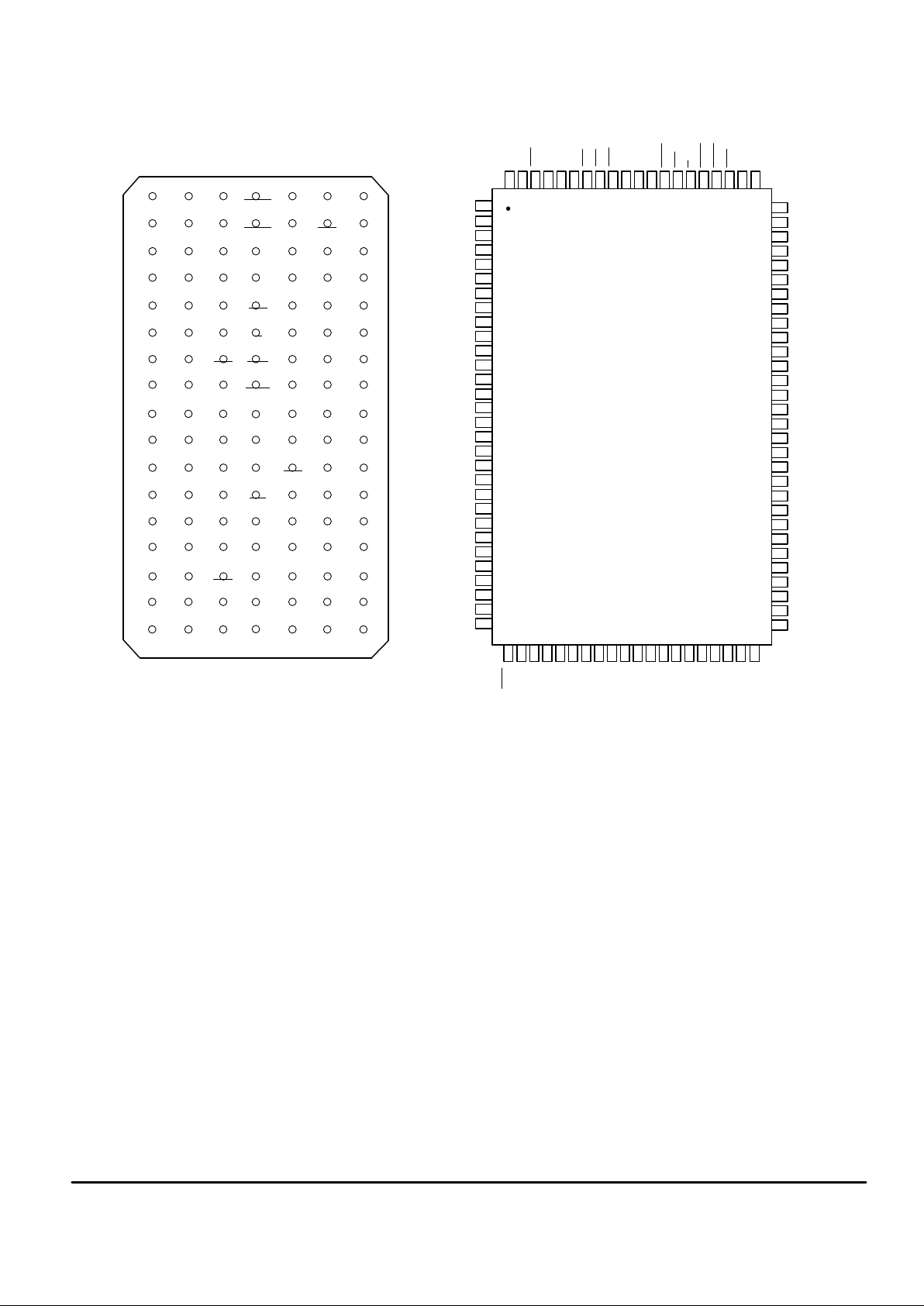
MCM63P736 TQFP PIN DESCRIPTIONS
Pin Locations Symbol
Type Description
85 ADSC Input Synchronous Address Status Controller: Active low, interrupts any
ongoing burst and latches a new external address. Used to initiate a
READ, WRITE, or chip deselect.
84 ADSP Input Synchronous Address Status Processor: Active low, interrupts any
ongoing burst and latches a new external address. Used to initiate a
new READ or chip deselect (exception — chip deselect does not occur
when ADSP
is asserted and SE1 is high).
83 ADV Input Synchronous Address Advance: Increments address count in
accordance with counter type selected (linear/interleaved).
(a) 51, 52, 53, 56, 57, 58, 59, 62, 63
(b) 68, 69, 72, 73, 74, 75, 78, 79, 80
(c) 1, 2, 3, 6, 7, 8, 9, 12, 13
(d) 18, 19, 22, 23, 24, 25, 28, 29, 30
DQx I/O Synchronous Data I/O: “x” refers to the byte being read or written
(byte a, b, c, d).
86 G Input Asynchronous Output Enable Input:
Low — enables output buffers (DQx pins).
High — DQx pins are high impedance.
89 K Input Clock: This signal registers the address, data in, and all control signals
except G
, LBO, and ZZ.
31 LBO Input Linear Burst Order Input: This pin must remain in steady state (this
signal not registered or latched). It must be tied high or low.
Low — linear burst counter (68K/PowerPC).
High — interleaved burst counter (486/i960/Pentium).
32, 33, 34, 35, 44, 45, 46,
47, 48, 49, 50, 81, 82, 99, 100
SA Input Synchronous Address Inputs: These inputs are registered and must
meet setup and hold times.
36, 37 SA1, SA0 Input Synchronous Address Inputs: these pins must be wired to the two LSBs
of the address bus for proper burst operation. These inputs are
registered and must meet setup and hold times.
93, 94, 95, 96
(a) (b) (c) (d)
SBx Input Synchronous Byte Write Inputs: “x” refers to the byte being written (byte
a, b, c, d). SGW
overrides SBx.
98 SE1 Input Synchronous Chip Enable: Active low to enable chip.
Negated high — blocks ADSP
or deselects chip when ADSC is
asserted.
97 SE2 Input Synchronous Chip Enable: Active high for depth expansion.
92 SE3 Input Synchronous Chip Enable: Active low for depth expansion.
88 SGW Input Synchronous Global Write: This signal writes all bytes regardless of the
status of the SBx
and SW signals. If only byte write signals SBx are
being used, tie this pin high.
87 SW Input Synchronous Write: This signal writes only those bytes that have been
selected using the byte write SBx
pins. If only byte write signals SBx
are being used, tie this pin low.
64 ZZ Input Sleep Mode: This active high asynchronous signal places the RAM into
the lowest power mode. The ZZ pin disables the RAMs internal clock
when placed in this mode. When ZZ is negated, the RAM remains in
low power mode until it is commanded to READ or WRITE. Data
integrity is maintained upon returning to normal operation.
15, 41, 65, 91 V
DD
Supply Core Power Supply.
4, 11, 20, 27, 54, 61, 70, 77 V
DDQ
Supply I/O Power Supply.
5, 10, 17, 21, 26, 40,
55, 60, 67, 71, 76, 90
V
SS
Supply Ground.
14, 16, 38, 39, 42, 43, 66 NC — No Connection: There is no connection to the chip.
MCM63P736•MCM63P818
6
MOTOROLA FAST SRAM
TOP VIEW 119 BUMP PBGA
6543217
B
C
V
SS
G
A
D
E
F
H
J
V
SS
V
SS
V
SS
V
SS
SA
V
SS
V
SS
V
SS
SA SA SA SA
SA SA SA SA
SA SA SA SA
NC
NC
NC
SA SA
NC
ZZ
SW
NC
NC
V
DDQ
V
DDQ
NC
V
DDQ
DQa
DQa
DQa
DQa
NCV
DD
NC
NC
NCNC
NC
NC
NC DQb VSSSA0
NC
LBO
NC
DQaSA1V
SS
NCDQb
V
DDQ
DQb V
SS
NC
NC
DQaSBa
V
SS
NCDQb
NC DQb V
SS
KV
SS
DQb
NC
V
DD
NCV
DD
NCV
DD
V
DDQ
NC VSSSGW
DQa
DQa
NCADV
SBbDQbNC
V
DDQ
NC V
SS
G
NCSE1V
SS
DQbNC
DQb NC VSSNC DQa
V
DD
NC
NC SE2 SA ADSC
ADSP
K
L
M
N
P
R
T
U
Not to Scale
V
DDQ
V
DDQ
SE3
V
DDQ
V
DDQ
NC
71
72
NC
V
DDQ
SA
69
70
66
67
68
64
65
61
62
63
3738343536 42433940 41 454644
60
59
58
57
56
55
54
53
52
51
31 3233
74
75
76
77
78
79
80
50494847
NC
NC
V
SS
DQa
NC
DQa
DQa
V
SS
V
DDQ
DQa
DQa
V
DDQ
V
SS
V
SS
V
DDQ
NC
NC
NC
DQb
DQb
DQb
DQb
NC
SASASE1
NC
K
NC
ADV
G
SA0
SASASA
SA
NC
NC
NC
LBO
SA1
V
DD
V
DD
NC
DQa
V
SS
DQa
DQa
NC
DQa
V
SS
V
DDQ
N
C
NC
V
SS
V
DDQ
NC
NC
DQb
V
DD
V
SS
V
SS
V
DDQ
DQb
DQb
DQb
DQb
NC
73
NC
94 93979695 89889291 90 86858710099 98 81828384
10
9
12
11
15
14
13
17
16
20
19
18
21
22
23
24
25
26
27
28
29
30
7
6
5
4
3
2
1
8
SA
SA
SW
SE2
SE3
VSSV
DD
ZZ
NC
V
DDQ
V
SS
NC
NC
NC
SA
SA
SASASA
SA
SA
TOP VIEW 100 PIN TQFP
NC
V
SS
ADSP
ADSC
SGW
SBa
SBb
MCM63P818 PIN ASSIGNMENTS
 Loading...