

Motorola MC141514T2, MC141514T1 Datasheet
MCM63P636
1
MOTOROLA FAST SRAM
Advance Information
64K x 36 Bit Pipelined BurstRAM
Synchronous Fast Static RAM
The MCM63P636 is a 2M–bit synchronous fast static RAM designed to provide
burstable, high performance, secondary cache for advanced microprocessors.
It is organized as 64K words of 36 bits each. This device integrates input registers, an output register, a 2–bit address counter, and a high speed SRAM onto
a single monolithic circuit for reduced parts count in cache data RAM applications. Synchronous design allows for precise cycle control with the use of an external clock (K) and external strobe clock (SK).
Addresses (SA), data inputs (DQx), and all control signals are clock (K)
controlled through positive–edge–triggered noninverting registers. Data strobes
STRBA, STRBA
, STRBB, and STRBB are strobe clock (SK) controlled through
positive–edge–triggered non–inverting registers. Strobe clock, 180 degrees out
of phase with clock (K), is only used with the data strobes such that they are
centered with data output on read cycles.
Burst sequences are initiated with ADS
input pin, and subsequent burst
addresses are generated internally by MCM63P636.
Write cycles are internally self–timed and are initiated with address and control
logic by the rising edge of the clock (K) input. This feature eliminates complex
off–chip write pulse generation and provides increased timing flexibility for
incoming signals. Special logic enables the memory to accept data on the rising
edge of clock (K) a cycle after address and control signals.
For read cycles, the SRAMs output data is temporarily stored by an
edge–triggered output register and then released to the output buffers at the
second rising edge of clock (K) for a read latency of three cycles. Data strobes
rise and fall with SRAM output to help external devices receiving the data to
latch the data.
The MCM63P636 operates from a 3.3 V core power supply, a 2.0 V input power
supply, and a 2.0 V I/O power supply . These power supplies are designed so that
power sequencing is not required.
• MCM63P636–250 = 3.9 ns Access/4 ns Cycle (250 MHz)
MCM63P636–225 = 4.3 ns Access/4.4 ns Cycle (225 MHz)
MCM63P636–200 = 4.9 ns Access/5 ns Cycle (200 MHz)
• 3.3 V ± 200 mV VDD Supply, 2.0 V V
DDI
and V
DDQ
Supply
• Internally Self–Timed Late Write Cycle
• Three–Cycle Single–Read Latency
• Strobe Clock Input and Data Strobe Output Pins
• On–Chip Output Enable Control
• On–Chip Burst Advance Control
• Four–Tick Burst
• Power–On Reset Pin
• Low Power Stop Clock Operation
• Boundary Scan (PBGA Only)
• JEDEC Standard 153–Pin PBGA and 100–Pin TQFP Packages
This document contains information on a new product. Specifications and information herein are subject to change without notice.
Order this document
by MCM63P636/D
MOTOROLA
SEMICONDUCTOR TECHNICAL DATA
MCM63P636
ZP PACKAGE
PBGA
CASE 1107–01
TQ PACKAGE
TQFP
CASE 983A–01
3/16/98
Motorola, Inc. 1998
MCM63P636
2
MOTOROLA FAST SRAM
PBGA
PIN ASSIGNMENT
153–BUMP PBGA
TOP VIEW
6543217
B
C
ADS
G
A
D
E
F
H
J
V
SS
K
V
SS
V
SS
NC
SA
SA
SA
V
DDQ
SA SE2 NC
V
SS
W
RESET
DQa SA SA0 SA
SA
V
SS
DQb
V
DDQ
SA
NC
V
DD
V
DD
V
DD
V
DDI
V
SS
STRBB
V
DDI
V
DD
STRBB
DQb
SA1SA
TCK
SA
TDIV
DDQ
DQa
DQa DQa DQa SA
V
SS
V
SS
SA
V
SS
V
SS
V
DD
V
DDQ
V
SS
DQa DQa V
DDI
V
SS
V
DD
V
SS
V
SS
V
DD
V
DDQ
V
SS
DQa DQa STRBA VDDNC
DQa
V
DD
V
SS
NU/V
SS
V
SS
V
SS
V
DDQ
V
SS
DQa STRBA
V
DD
V
DD
V
DD
DQa V
DDIVDD
V
SS
V
SS
V
DD
V
DDQ
V
SS
DQa DQa V
DD
DQa V
DD
NU/V
SS
V
SS
DQa DQa SA SE3
SE1
K
L
M
N
P
R
T
U
V
SS
SA
NU/V
DD
V
SS
V
DDQ
V
SS
89
DQb
DQb
V
SS
DQb
V
DDQ
TDO
DQb
V
SS
V
SS
DQb
V
SS
DQb
DQb
V
SS
DQb
DQbDQb
V
DDQ
DQb
DQb
V
DDQ
DQb
DQb
DQb
V
SS
DQb
V
SS
V
SS
V
DDQ
V
DDQ
V
DDQ
V
DDQ
DQa
VSSV
DDQVDD
SK VSSVDDV
DDQVSS
V
DDQ
TMS TRST
MCM63P636
3
MOTOROLA FAST SRAM
TQFP
PIN ASSIGNMENT
71
72
DQa
DQb
69
70
66
67
68
64
65
61
62
63
37 3834 35 36 42 4339 40 41 45 4644
60
59
58
57
56
55
54
53
52
51
31 32 33
74
75
76
77
78
79
80
50494847
DQb
DQb
V
SS
DQb
DQb
DQb
DQb
V
SS
DQb
DQb
V
DDQ
V
SS
V
SS
DQa
DQa
DQa
DQa
DQa
DQa
DQa
STRBA
SASASE1
K
NU/V
NC
ADS
RESET
SA0
SASASA
SA
NCVNC
DDI
V
SS
NC
SA1
V
DD
V
DD
STRBB
DQb
V
SS
DQb
DQb
DQb
DQb
V
SS
DQb
DQb
V
SS
DQb
DQb
DQa
V
DD
V
SS
V
SS
DQa
DQa
DQa
DQa
DQa
73
DQa
94 9397 96 95 89 8892 91 90 86 8587100 99 98 81828384
10
9
12
11
15
14
13
17
16
20
19
18
21
22
23
24
25
26
27
28
29
30
7
6
5
4
3
2
1
8
SA
SA
V
SE2
SK
SE3
VSSV
DD
W
STRBB
STRBA
V
SS
DQa
DQa
DQa
SA
NC
SASASA
SA
SA
V
DDQ
V
DDQ
V
DDQ
V
DDQ
V
DDQ
V
DDQ
V
DDQ
DDI
V
DDI
V
DDI
DD
NU/VSSNU/V
SS
MCM63P636
4
MOTOROLA FAST SRAM
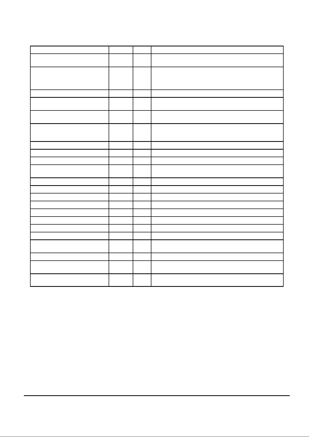
PBGA PIN DESCRIPTIONS
Pin Locations Symbol
Type Description
5D ADS Input Synchronous Address Status: Active low, used to initiate read or write
state machines latch in external addresses, or deselect chip.
(a) 1B, 2B, 1D, 2D, 3D, 1F, 2F, 1H, 2H,
1K, 2K, 1M, 2M, 1P, 2P, 3P, 1T, 2T
(b) 8B, 9B, 7D, 8D, 9D, 8F, 9F, 8H, 9H,
8K, 9K, 8M, 9M, 7P, 8P, 9P, 8T, 9T
DQx I/O Synchronous Data I/O: “x” refers to the word being read or written
(I/Os a and b).
5F K Input Clock: This signal registers the address, data in, and all control signals.
6C RESET Input Asynchronous Power–On Reset: Active low at power up, resets internal
state machines.
3A, 7A, 3B, 7B, 5M, 5N,
4P, 5P, 6P, 4R, 6R, 3T, 4T, 6T
SA Input Synchronous Address Inputs: These inputs are registered and must
meet setup and hold times.
5R, 5T SA1, SA0 Input Synchronous Address Inputs: These pins must be wired to the two
LSBs of the address bus for proper burst operation. These inputs are
registered and must meet setup and hold times.
4A SE1 Input Synchronous Chip Enable: Active low to enable chip.
5A SE2 Input Synchronous Chip Enable: Active high to enable chip.
4B SE3 Input Synchronous Chip Enable: Active low to enable chip.
5G SK Input Data Strobe Clock: 180 degrees out–of–phase with K. Used only with
data strobes.
3K STRBA Output Data Strobe: Used in reference to DQa I/Os.
3H STRBA Output Data Strobe: Used in reference to DQa I/Os.
7K STRBB Output Data Strobe: Used in reference to DQb I/Os.
7H STRBB Output Data Strobe: Used in reference to DQb I/Os.
5U TCK Input Boundary Scan Pin, Test Clock: If boundary scan is not used, TCK
must be tied to VDD or VSS.
3U TDI Input Boundary Scan Pin, T est Data In.
7U TDO Output Boundary Scan Pin, Test Data Out.
4U TMS Input Boundary Scan Pin, Test Mode Select.
6U TRST Input Boundary Scan Pin, Asynchronous T est Reset. If boundary scan is not
used, TRST
must be tied to VSS.
5C W Input Synchronous Write.
4D, 6D, 3E, 7E, 4F, 6F, 3G, 7G,
4H, 6H, 4K, 6K, 3L, 7L, 4M, 6M, 3N, 7N
V
DD
Supply Core Power Supply.
3F, 7F, 3M, 7M V
DDI
Supply Input Power Supply.
2A, 8A, 2C, 8C, 2E, 8E, 2G, 8G,
2J, 8J, 2L, 8L, 2N, 8N, 2R, 8R, 2U, 8U
V
DDQ
Supply I/O Power Supply.
1A, 9A, 1C, 3C, 7C, 9C, 1E, 4E, 5E,
6E, 9E, 1G, 4G, 6G, 9G, 5H, 1J, 3J,
4J, 6J, 7J, 9J, 1L, 4L, 5L, 6L, 9L, 1N,
4N, 6N, 9N, 1R, 3R, 7R, 9R, 1U, 9U
V
SS
Supply Ground.
6A, 5B, 5K, 7T NC — No Connection: There is no connection to the chip.
6B NU/V
DD
— Not Usable: There is an internal connection to the chip. This pin may be
left unconnected or tied to VDD.
4C, 5J NU/V
SS
— Not Usable: There is an internal connection to the chip. This pin may be
left unconnected or tied to VSS.
MCM63P636
5
MOTOROLA FAST SRAM
TQFP PIN DESCRIPTIONS
Pin Locations Symbol
Type Description
85 ADS Input Synchronous Address Status: Active low, used to initiate read or write
state machines latch in external addresses, or deselect chip.
(a) 1, 2, 3, 6, 7, 8, 9, 12, 13, 18,
19, 22, 23, 24, 25, 28, 29, 30
(b) 51, 52, 53, 56, 57, 58, 59, 62, 63,
68, 69, 72, 73, 74, 75, 78, 79, 80
DQx I/O Synchronous Data I/O: “x” refers to the word being read or written
(I/Os a and b).
89 K Input Clock: This signal registers the address, data in, and all control signals.
84 RESET Input Asynchronous Power–On Reset: Active low at power up, resets internal
state machines.
32, 33, 34, 35, 44, 45, 46,
47, 48, 49, 81, 82, 99, 100
SA Input Synchronous Address Inputs: These inputs are registered and must
meet setup and hold times.
36, 37 SA1, SA0 Input Synchronous Address Inputs: These pins must be wired to the two
LSBs of the address bus for proper burst operation. These inputs are
registered and must meet setup and hold times.
98 SE1 Input Synchronous Chip Enable: Active low to enable chip.
97 SE2 Input Synchronous Chip Enable: Active high to enable chip.
92 SE3 Input Synchronous Chip Enable: Active low to enable chip.
93 SK Input Data Strobe Clock: 180 degrees out–of–phase with K. Used only with
data strobes.
16 STRBA Output Data Strobe: Used in reference to DQa I/Os.
14 STRBA Output Data Strobe: Used in reference to DQa I/Os.
64 STRBB Output Data Strobe: Used in reference to DQb I/Os.
66 STRBB Output Data Strobe: Used in reference to DQb I/Os.
88 W Input Synchronous Write.
15, 41, 65, 91 V
DD
Supply Core Power Supply.
38, 43, 87, 94 V
DDI
Supply Input Power Supply.
4, 11, 20, 27, 54, 61, 70, 77 V
DDQ
Supply I/O Power Supply.
5, 10, 17, 21, 26, 40,
55, 60, 67, 71, 76, 90
V
SS
Supply Ground.
31, 39, 42, 50, 86 NC — No Connection: There is no connection to the chip.
83 NU/V
DD
— Not Usable: There is an internal connection to the chip. This pin may be
left unconnected or tied to VDD.
95, 96 NU/V
SS
— Not Usable: There is an internal connection to the chip. This pin may be
left unconnected or tied to VSS.
MCM63P636
6
MOTOROLA FAST SRAM
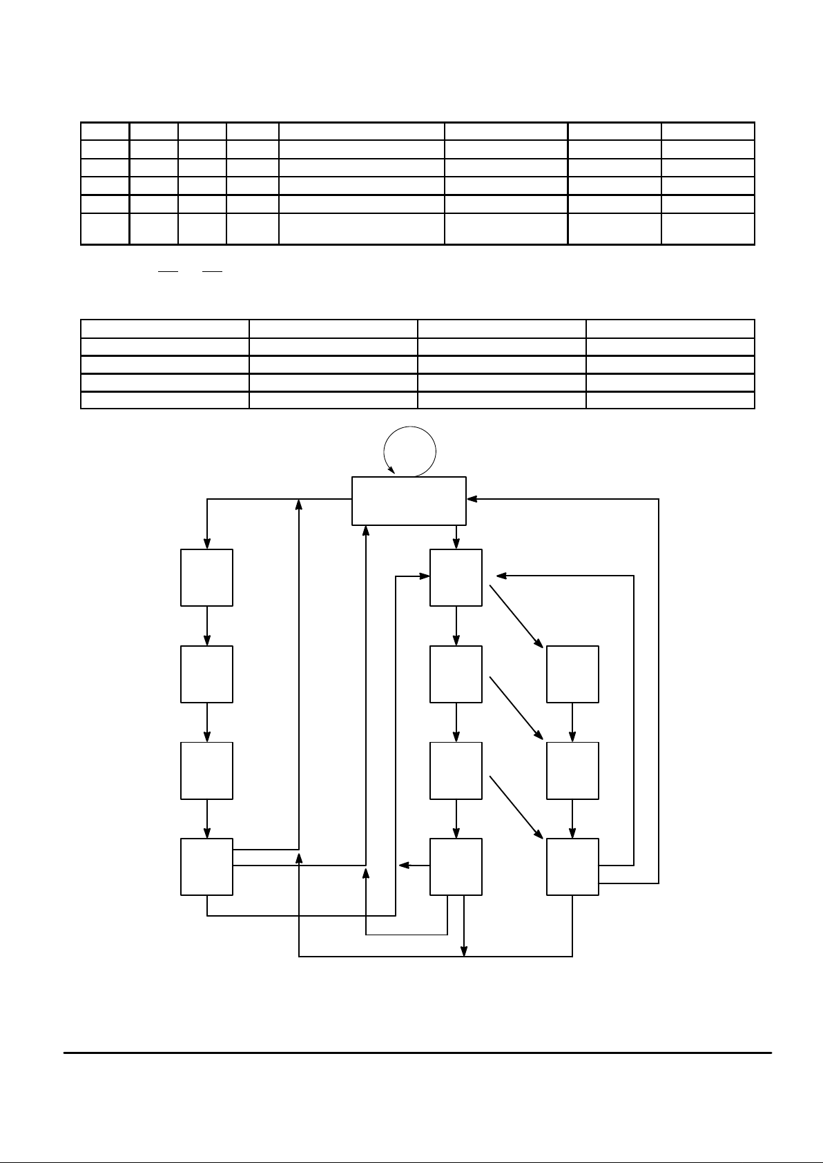
TRUTH TABLE (See Notes 1 and 2)
K
E ADS W Next Cycle (n) Input Command Code DQ (n + 1) DQ (n+2)
L – H False 0 X Deselect D High–Z —
L – H True 0 0 Load Address, Begin Write BW Data In —
L – H True 0 1 Load Address, Begin Read BR — Data Out
L – H X 1 0 Continue W rite CW Data In —
L – H X 1 1 Continue Read
Mask Write
CR
MW
—
High–Z
Data Out
—
NOTES:
1. X = don’t care, 1 = logic high, 0 = logic low.
2. E = true if SE1
and SE3 = 0, and SE2 = 1.
BURST ADDRESS TABLE
1st Address (External) 2nd Address (Internal) 3rd Address (Internal) 4th Address (Internal)
X . . . X00 X . . . X01 X . . . X10 X . . . X11
X . . . X01 X . . . X00 X . . . X1 1 X . . . X10
X . . . X10 X . . . X11 X . . . X00 X . . . X01
X . . . X11 X . . . X10 X . . . X01 X . . . X00
DESELECT
NEW
READ*
Figure 1. Functional State Diagram
BURST
READ 1*
BURST
READ 2*
BURST
READ 3*
NEW
WRITE*
BURST
WRITE 1*
BURST
WRITE 2*
BURST
WRITE 3*
MASKED
WRITE 1*
MASKED
WRITE 2*
MASKED
WRITE 3*
D, CW, CR – MW
BR
BW
CR
CR
CR
BR
BW
BW
D, CW, MW
CW
CW
CW
BR
MW
MW
MW
MW
MW
BR
BW
D, CW, MW
D, CW, MW
*Command code inputs not shown from this state are not valid.
MCM63P636
7
MOTOROLA FAST SRAM
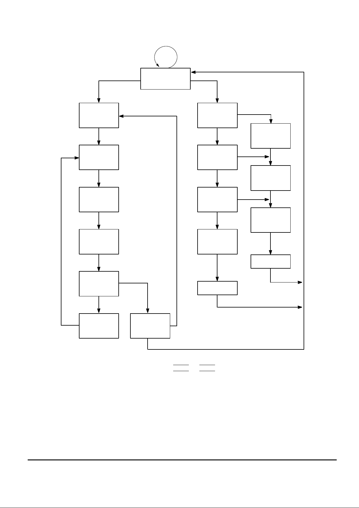
HIGH–Z
4
INTERMEDIATE
HIGH–Z1,
4
Figure 2. Data I/O State Diagram
D, CW, CR – MW
BR
CR
CR
CR
D, CW, CR
CW, MW
MW
CW, MW
NOTES:
1. Command code inputs not shown from this state are not valid.
2. STRBA and STRBB transition from logic 1 to 0. STRBA
and STRBB transition from logic 0 to 1.
3. STRBA and STRBB transition from logic 0 to 1. STRBA
and STRBB transition from logic 1 to 0.
4. Data strobes are driven to High–Z.
INTERMEDIA TE
HIGH–Z1,
4
DATA–OUT/
Q(1)VALID1,
2
DATA–OUT/
Q(2)VALID1,
3
DATA–OUT/
Q(3)VALID1,
2
DATA–OUT/
Q(4)VALID1,
3
DATA–OUT/
Q(4)VALID1,
3
DATA–IN (1)/
HIGH–Z1,
4
CW
CW
CW
DATA–IN (2)/
HIGH–Z1,
4
DATA–IN (3)/
HIGH–Z1,
4
DATA–IN (4)/
HIGH–Z1,
4
MASK (2)/
HIGH–Z1,
4
MW
MW
MW
MASK (3)/
HIGH–Z1,
4
MASK (4)/
HIGH–Z1,
4
HIGH–Z1,
4
MW
MW
MW
HIGH–Z1,
4
BR
CR
BR
CR
BW
CR
MCM63P636
8
MOTOROLA FAST SRAM
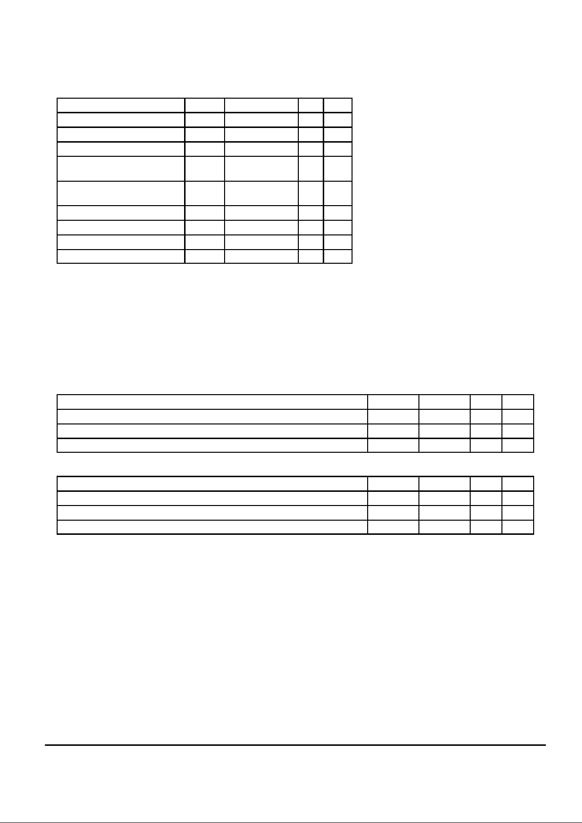
ABSOLUTE MAXIMUM RATINGS (See Note 1)
Rating Symbol Value Unit Notes
Power Supply Voltage V
DD
VSS – 0.5 to + 4.0 V
I/O Supply Voltage V
DDQ
VSS – 0.5 to 2.5 V 2, 3
Input Supply Voltage V
DDI
VSS – 0.5 to 2.5 V 2, 3
Voltage Relative to VSS for Any Pin
Except V
DD
V
in
VSS – 0.5 to
V
DDI
+ 0.5
V 2, 4
Input Voltage (Three–State I/O) V
IT
VSS – 0.5 to
V
DDQ
+ 0.5
V 2, 4
Output Current (per I/O) I
out
± 20 mA
Package Power Dissipation P
D
2.75 W 5
Temperature Under Bias T
bias
– 10 to 85 °C
Storage Temperature T
stg
– 55 to 125 °C
NOTES:
1. Permanent device damage may occur if ABSOLUTE MAXIMUM RATINGS are
exceeded. Functional operation should be restricted to RECOMMENDED OPERATING CONDITIONS. Exposure to higher than recommended voltages for extended
periods of time could affect device reliability.
2. This is a steady–state DC parameter that is in effect after the power supply has
achieved its nominal operating level. Power sequencing is not necessary.
3. V
DDI
= V
DDQ
.
4. Max Vin and VIT are not to exceed Max VDD.
5. Power dissipation capability is dependent upon package characteristics and use
environment. See Package Thermal Characteristics.
PACKAGE THERMAL CHARACTERISTICS — PBGA
Rating Symbol Max Unit Notes
Junction to Ambient (@ 200 lfm) R
θJA
25 °C/W 1, 2
Junction to Board (Bottom) R
θJB
12 °C/W 3
Junction to Case (Top) R
θJC
10 °C/W 4
PACKAGE THERMAL CHARACTERISTICS — TQFP
Rating Symbol Max Unit Notes
Junction to Ambient (@ 200 lfm) R
θJA
25 °C/W 1, 2
Junction to Board (Bottom) R
θJB
17 °C/W 3
Junction to Case (Top) R
θJC
9 °C/W 4
NOTES:
1. Junction temperature is a function of on–chip power dissipation, package thermal resistance, mounting site (board) temperature, ambient
temperature, air flow, and board thermal resistance.
2. Per SEMI G38–87.
3. Indicates the average thermal resistance between the die and the printed circuit board.
4. Indicates the average thermal resistance between the die and the case top surface via the cold plate method (MIL SPEC–883 Method 1012.1).
This device contains circuitry to protect the
inputs against damage due to high static voltages or electric fields; however, it is advised
that normal precautions be taken to avoid
application of any voltage higher than maximum rated voltages to this high–impedance
circuit.
MCM63P636
9
MOTOROLA FAST SRAM
DC OPERA TING CONDITIONS AND CHARACTERISTICS
(VDD = 3.3 V ± 200 mV, TA = 0 to 70°C, Unless Otherwise Noted)
RECOMMENDED OPERATING CONDITIONS AND DC CHARACTERISTICS (Voltage Referenced to V
SS
= 0 V)
Parameter Symbol Min Typ Max Unit
Supply Voltage V
DD
3.1 3.3 3.5 V
Input Supply Voltage V
DDI
1.8 — 2.2 V
I/O Supply Voltage V
DDQ
1.8 — 2.2 V
Input Low Voltage (V
DDI
= V
DDQ
) V
IL
– 0.5 — 0.35 x V
DDI
V
Input High Voltage (V
DDI
= V
DDQ
) V
IH
0.65 x V
DDI
— V
DDI
+ 0.5 V
Input Leakage Current (0 V ≤ Vin ≤ VDD) I
lkg(I)
— — ± 1 µA
Output Leakage Current (0 V ≤ Vin ≤ V
DDQ
) I
lkg(O)
— — ± 1 µA
Output Low Voltage (IOL = 1 mA) V
OL
– 0.5 — 0.4 V
Output High Voltage (IOL = – 1 mA) V
OH
V
DDQ
– 0.4 — V
DDQ
+ 0.5 V
V
IH
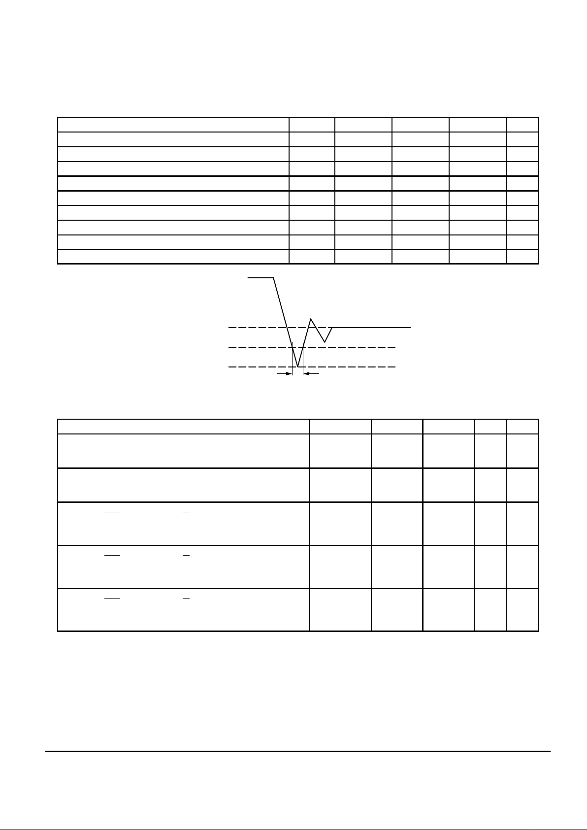
20% t
KHKH
V
SS
VSS – 0.5 V
Figure 3. Undershoot Voltage
VSS – 0.25 V
SUPPLY CURRENTS
Parameter Symbol Min Max Unit Notes
AC Supply Current (Device Selected, All Outputs Open,
Freq = Max, VDD = Max)
I
DDA
– 250
I
DDA
– 225
I
DDA
– 200
— TBD mA 1, 2,
3, 4
Input and I/O Supply Current – Desktop (All 40 Outputs Toggling,
Freq = Max, V
DDI
= Max, V
DDQ
= Max, V
DDI
= V
DDQ
, Cdt = 24 pF)
I
DDQ
– 250
I
DDQ
– 225
I
DDQ
– 200
— 311
280
249
mA 2, 5
Static Standby Supply Current (Device Deselected, Freq = Max,
VDD = Max, ADS
≥ (V
DDI
– 0.2 V), W Static ≤ (VSS + 0.2 V)
or ≥ (V
DDI
– 0.2 V), SA and DQx Inputs Static ≤ (VSS + 0.2 V),
Outputs Disabled)
I
SB1
– 250
I
SB1
– 225
I
SB1
– 200
— 63
57
50
mA 1, 2, 4
Idle Standby Supply Current (Device Deselected, Freq = 0,
VDD = Max, ADS
≥ (V
DDI
– 0.2 V), W Static ≤ (VSS + 0.2 V)
or ≥ (V
DDI
– 0.2 V), SA and DQx Inputs Static ≤ (VSS + 0.2 V),
Outputs Disabled)
I
SB2A
— TBD mA 1, 3, 4
Idle Input Standby Supply Current (Device Deselected, Freq = 0,
VDD = Max, ADS
≥ (V
DDI
– 0.2 V), W Static ≤ (VSS + 0.2 V)
or ≥ (V
DDI
– 0.2 V), SA and DQx Inputs Static ≤ (VSS + 0.2 V),
Outputs Disabled)
I
SB2B
— TBD mA 1, 3, 5
NOTES:
1. Device is selected and deselected as defined by the Truth Table.
2. Reference AC Operating Conditions and Characteristics for input and timing.
3. Data states are all zero.
4. Includes supply current for VDD only.
5. Includes supply currents for V
DDI
and V
DDQ
only.
 Loading...