

Motorola MC141511AT2, MCC141511A Datasheet
3–19
MC141511AMOTOROLA
LCD Segment Driver
CMOS
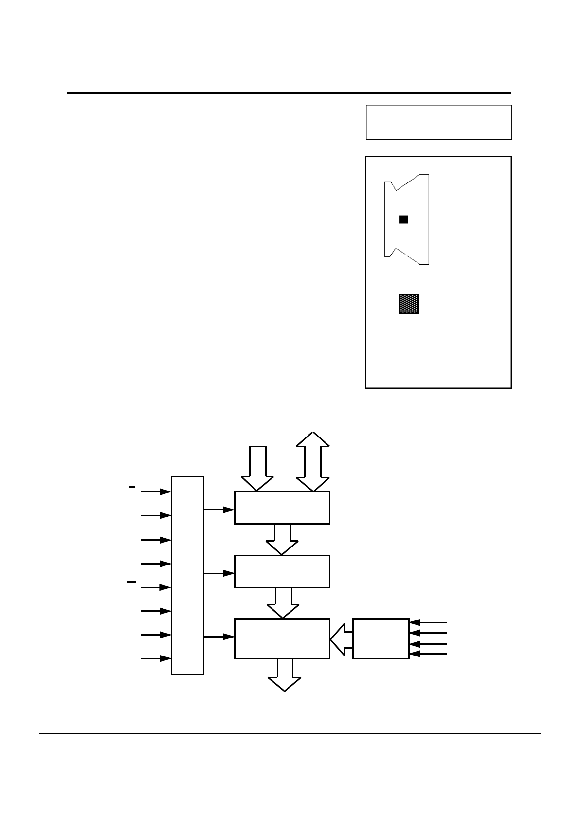
The MC141511A is an LCD frontplane (segment) driver chip which includes a 656 x 8 display RAM. The MC68HC05L10 microcomputer is the
companion device which provides the backplane drive.
The MC68HC05L10, together with one MC141511A, may be used to
drive a 5248-pixel muxed-by-41 display or a 4096-pixel muxed-by-32 display. Larger displays may be driven by adding additional MC141511A.
The MC141511A is a low operating voltage version of MC141511. It is
pin to pin compatible to the MC141511.
See Application Note AN-HK-13A.
• Operating Supply Voltage Range -
Control Logic, RAM, and Latch (VDD Pin): 2.7V to 5.5V
Frontplane Drivers (VLCD Pin): 4.5V to 13.2V
• Operating Temperature Range: -20 to 70˚C
• Direct Interface with the MC68HC05L10
• 656 x 8 Static RAM (Display RAM)
• 128 LCD Segment (Frontplane) Driving Signals
• 10-Bit Address Bus and 8-Bit Bidirectional Data Bus
• Selectable 1:32 or 1:41 Multiplex Ratios
• Available in Two Forms:
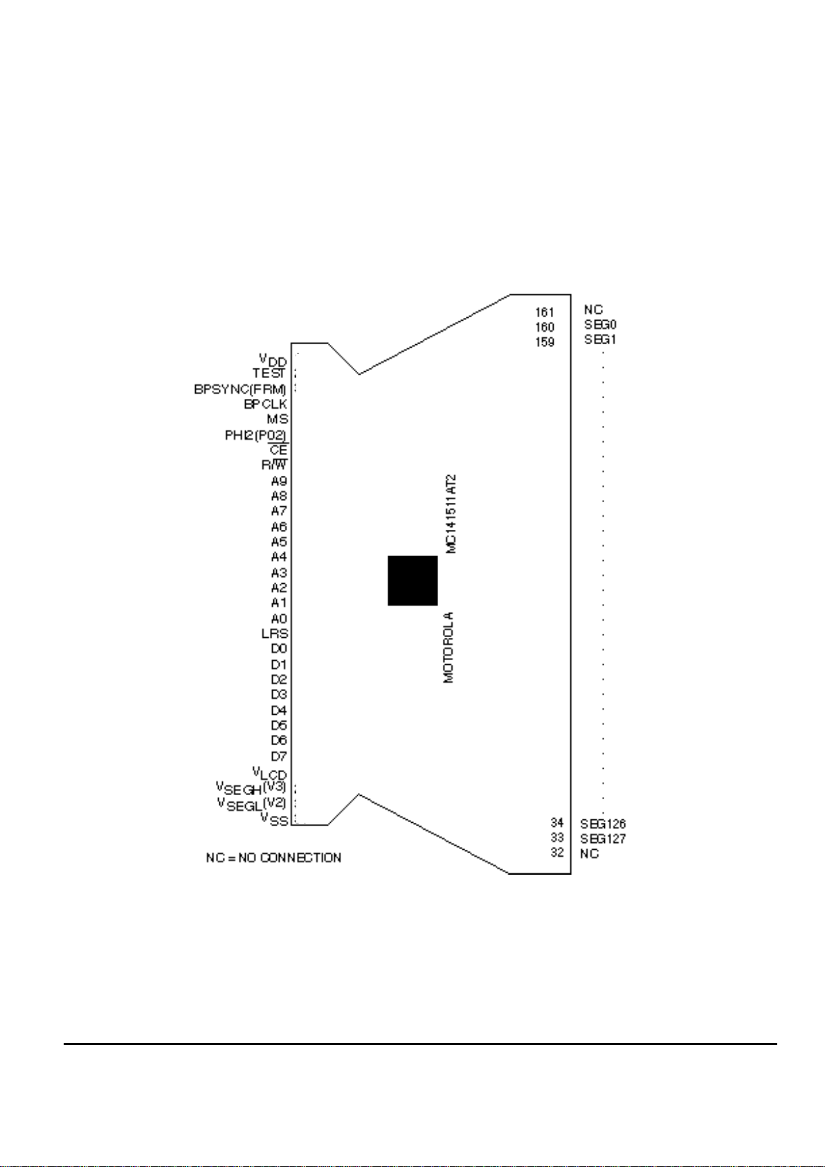
TAB (Tape Automated Bonding), 161 Contacts, 10 sprocket hole device
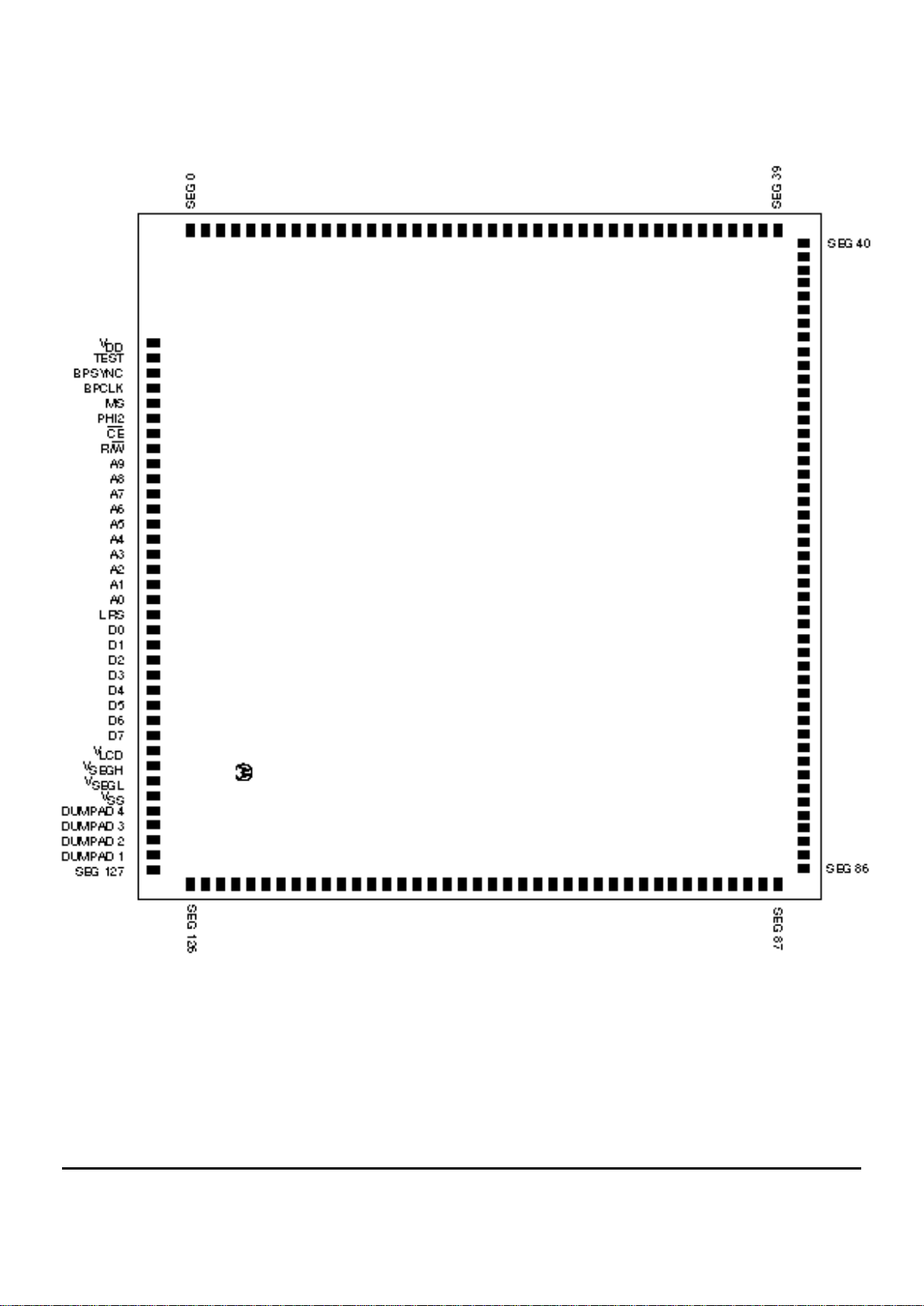
Die Form Without Gold Bumps, 159 Pads with 4.5 mil Pads Pitch
Control Logic
Display RAM
LCD D ATALATCH
SEGMENT DRIVER
A0-A9
D0-D7
V
LCD
V
SEGH
V
SEGL
V
SS
R/W
BPCLK
CE
LRS
PHI2
BPSYNC
DRIVER OUTP UTS
MS
VDD
LEVEL
SELECTOR
BLOCK DIAGRAM
MC141511A
MC141511AT2
TAB
MCC141511A
DIE
ORDERING INFORMATION
MCC141511A BARE DIE
MC141511AT2 TAB
MOTOROLA
SEMICONDUCTOR TECHNICAL DATA
REV 3
10/96
MOTOROLA
3–20
MC141511A
Figure 1A. TAB Package Contact Assignment (Copper View)
1
2
3
4
5
6
7
8
9
10
11
12
13
14
15
16
17
18
19
20
21
22
23
24
25
26
27
28
29
30
31
3–21
MC141511AMOTOROLA
Figure 1B. Chip Pad Assignment
MOTOROLA
3–22
MC141511A
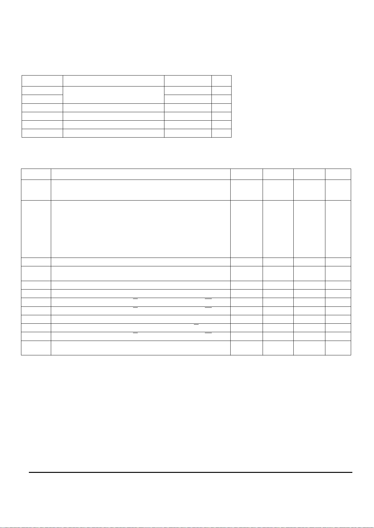
Symbol Parameter Value Unit
V
DD
Supply Voltage -0.3 to +7.0 V
V
LCD
-0.3 to +14.0 V
V
in
Input Voltage VSS-0.3 to VDD+0.3 V
I Current Drain Per Pin Excluding VDD and V
SS
25 mA
T
A
Operating Temperature -20 to +70 ˚C
T
stg
Storage Temperature Range -65 to +150 ˚C
MAXIMUM RATINGS*(Voltages Referenced to VSS, TA = 25˚C)
* Maximum Ratings are those values beyond which damage to the device may occur. Functional
operation should be restricted to the limits in the Electrical Characteristics tables or Pin Description
section.
Symbol Parameter Min Typ Max Unit
V
DD
V
LCD
Operating Voltage
Supply Voltage
LCD Voltage
2.7
4.5
-
-
5.5
13.2
V
V
I
AC
I
DP
I
SB
I
AC
I
DP
I
SB
Supply Current
at VDD=5.5V (PHI2=3.685MHz)
ACCESS
DISPLAY
STANDBY (Using DON bit of the MCU)
at VDD=3.0V (PHI2=1.25MHz)
ACCESS
DISPLAY
STANDBY (Using DON bit of the MCU)
-
-
-
-
-
-
25
15
17
10
200
30
20
200
30
20
uA
uA
uA
uA
uA
uA
I
LCD
Supply Current at V
LCD
- - 200 uA
V
OL
V
OH
Output Voltage, Iload10.0uA -
V
LCD
-0.1
-
-
0.1
-
V
V
V
OH
Output High Voltage (Iload=1.6mA) D7-D0 VDD-0.8 - - V
V
OL
Output Low Voltage (Iload=1.6mA) D7-D0 - - 0.4 V
V
IH
Input High Voltage R/W, BPCLK, BPSYNC, PHI2, MS, CE, D7-D0 0.8xV
DD
-VDDV
V
IL
Input Low Voltage R/W, BPCLK, BPSYNC, PHI2, MS, CE, D7-D0 V
SS
- 0.2xV
DD
V
V
R
Data Retention 2.0 - - V
I
in
Input Current BPCLK, BPSYNC, R/W, PHI2, D7-D0 - - 1 uA
C
in
Capacitance R/W, BPCLK, BPSYNC, PHI2, MS, CE, D7-D0 - - 8 pF
I
OH
I
OL
Output current (VOH=4.5V, VOL=0.5V) D7-D0 +20
-
-
-
-
-20
uA
uA
ELECTRICAL CHARACTERISTICS (Voltage Referenced to VSS, TA= 25˚C)
This device contains circuitry to protect the inputs
against damage due to high static voltages or electric fields; however, it is advised that normal precautions to be taken to avoid application of any voltage
higher than maximum rated voltages to this high
impedance circuit. For proper operation it is recommended that Vin and V
out
be constrained to the
range VSS < or = (Vin or V
out
) < or = VDD. Reliability
of operation is enhanced if unused input are connected to an appropriate logic voltage level (e.g.,
either VSS or VDD). Unused outputs must be left
open. This device may be light sensitive. Caution
should be taken to avoid exposure of this device to
any light source during normal operation. This
device is not radiation protected.
3–23
MC141511AMOTOROLA
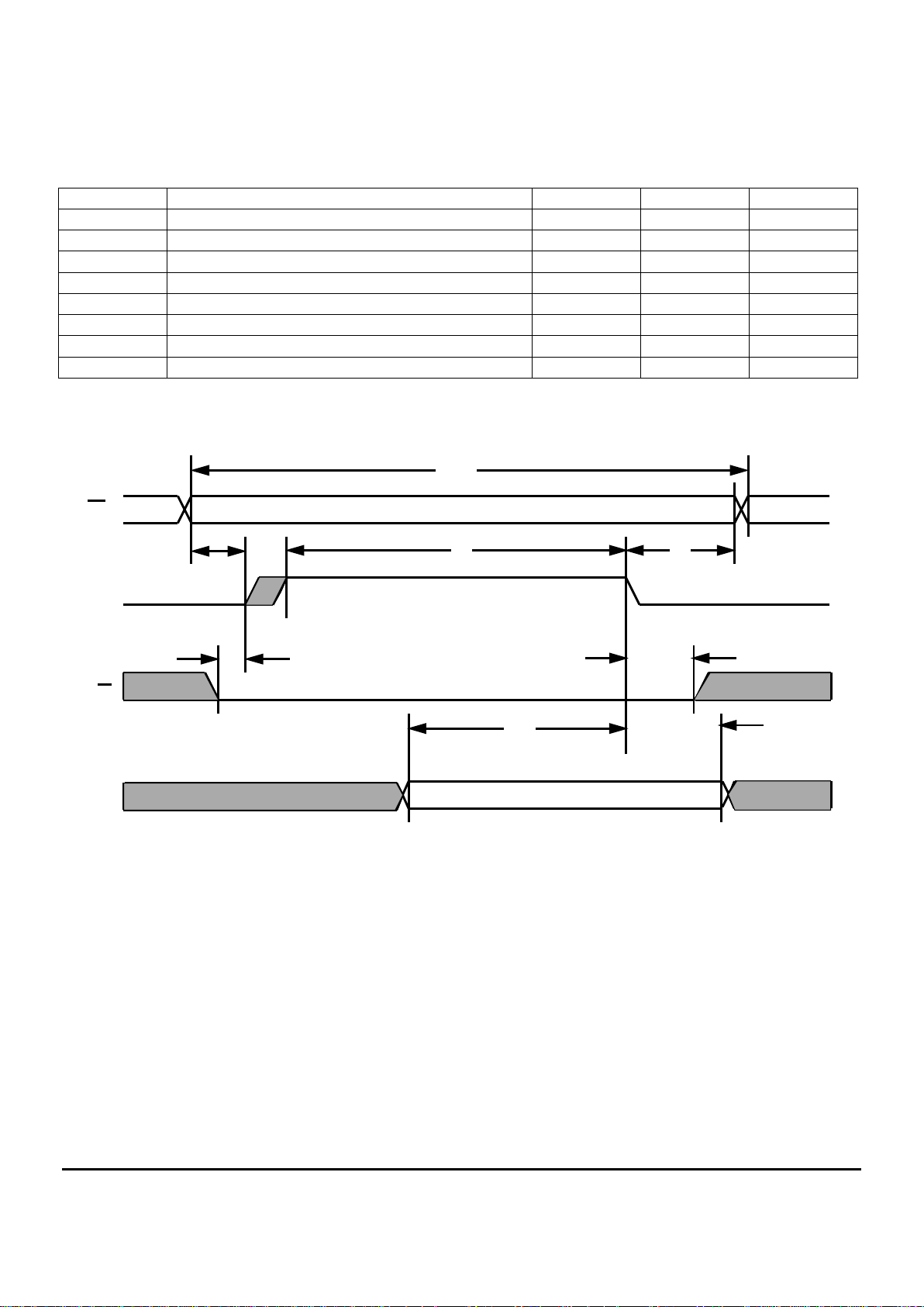
AC ELECTRICAL CHARACTERISTICS - WRITE CYCLE (VDD=3.0V
10±
%, V
SS
=0V)
Symbol Parameter Min Max Unit
t
CYCW
Write Cycle Time 400 - ns
t
AS
Address Set Up Time 100 - ns
t
AH
Address Hold Time 70 - ns
t
CS
Chip Select Pulse Width 260 - ns
t
WCS
Write to Chip Select Delay Time 100 - ns
t
DSW
Data Setup Time 200 - ns
t
H
Input Hold Time 15 - ns
t
WH
Write Hold Time from Chip Select 70 - ns
Figure 2. Write Cycle Timing
CE
PHI2
R/W
D0-7
t
CYCW
t
AS
t
CS
t
AH
t
WH
t
WCS
t
DSW
t
H
Data in Stable
MOTOROLA
3–24
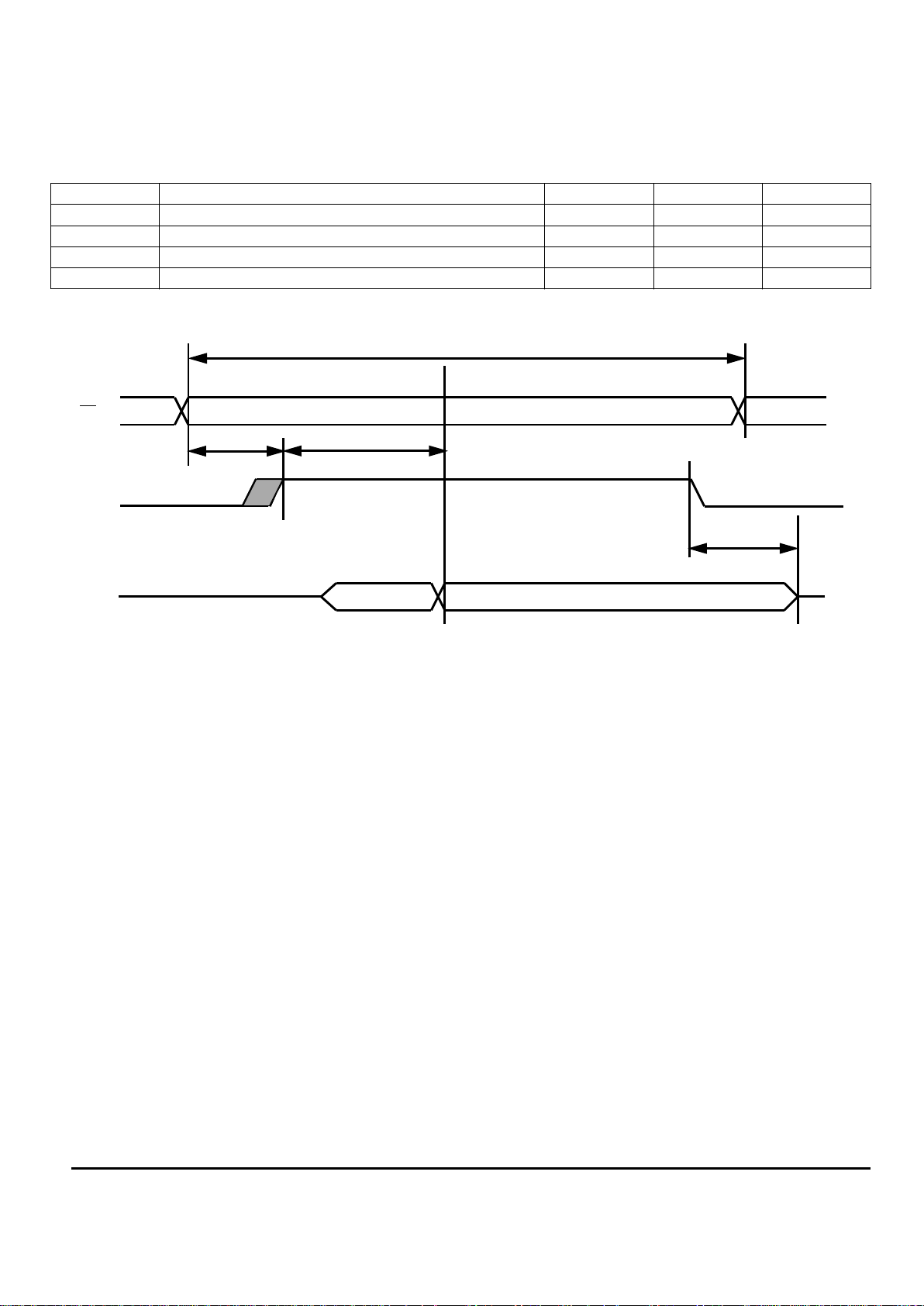
MC141511A
AC ELECTRICAL CHARACTERISTICS - READ CYCLE (VDD=3.0V
10±
%, V
SS
=0V)
Symbol Parameter Min Max Unit
t
CYCR
READ Cycle Time 400 - ns
t
AS
Address Setup Time 100 - ns
t
DDR
Data Delay Time (Read) - 350 ns
t
H
Output Hold Time 10 - ns
Figure 3. Read Cycle Timing
CE
PHI2
t
CYCR
t
DDR
D0-7
Data Valid
t
AS
t
H
 Loading...