

SEMICONDUCTOR TECHNICAL DATA
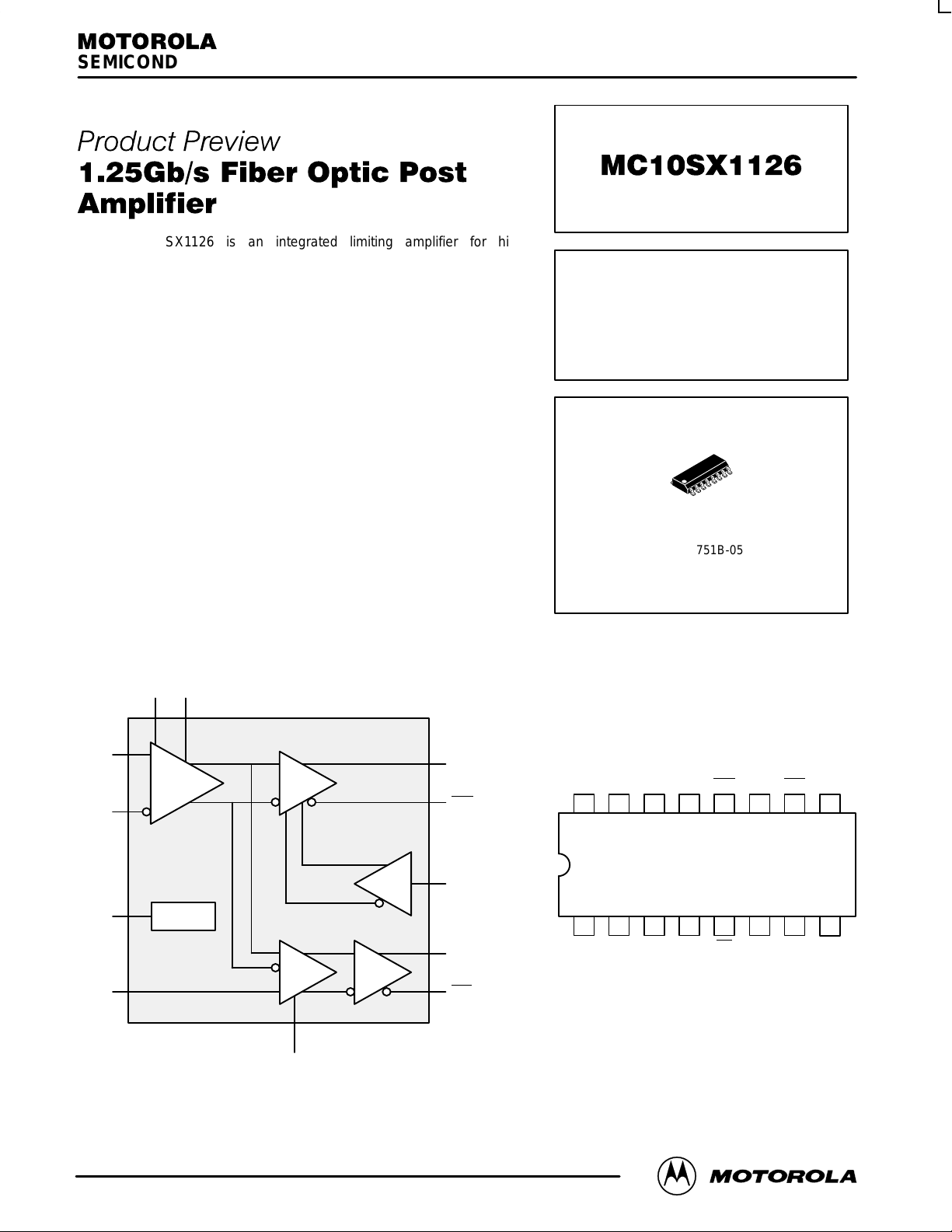
The MC10SX1126 is an integrated limiting amplifier for high
frequency fiber optic applications. The device interfaces directly to the
trans–impedance amplifier of a typical optical to electrical conversion
portion of a fiber optic link. With data rate capabilities in the 1.25Gb/s
range, the high gain limiting amplification of the SX1126 is ideal for high
speed fiber optic applications like SONET/SDM, ATM, FDDI, Fibre
Channel or Serial Hippi. The device is functionally and pin compatible to
the Signetics SA5225 with a significantly higher bandwidth. The C
and C
inputs to the limiting amplifier provide an auto-zero function to
AZN
effectively cancel any input offset voltage present in the amplifier.
The SX1126 incorporates a programmable level detect function to
identify when the input signal has been lost. This information can be fed
back to the Disable input of the device to maintain stability under loss of
signal conditions. Using the V
pin the sensitivity of the level detect
set
can be adjusted. The CLD input is used to filter the level detect input so
that random noise spikes are filtered out.
The MC10SX1 126 is compatible with MECL10H logic levels.
• Wideband Operation: 50MHz to 900MHz
• Programmable Input Signal Level Detection
• Operation with single +5V or standard ECL supply
• Standard 16-lead SOIC Package
• Fully Differential Design to Minimize Noise Affects
• 10KH Compatible
AZP
FIBER OPTIC
POST AMPLIFIER
D SUFFIX
PLASTIC SOIC PACKAGE
CASE 751B-05
C
AZPCAZN
D
in
Limiting
Amplifier
D
in
V
ref
V
set
Reference
ECL
Buffer
Level
Detect
C
LD
Disable
ECL
Buffer
D
out
D
out
Disable
LOS
LOS
V
set
C
AZNCAZP
Figure 1. MC10SX1126 Block Diagram
This document contains information on a product under development. Motorola reserves the right to change or
discontinue this product without notice.
V
refVCCEDout
1516 14 13 12 11 10
21 34567
GNDADinD
GNDELOS LOS
D
out
inVCCACLD
9
8
Disable
Figure 2. 16–Lead Pinout
(Top View)
4/98
Motorola, Inc. 1998
1
REV 0.1
MC10SX1126
FUNCTION TABLE
Pin Function
C
AZN
C
AZP
GND
A
Din, D
in
V
CCA
C
LD
Disable When asserted LOW, or left open and pulled LOW via the input pulldown resistor , the output buffer will be enabled and will
LOS Loss of signal. This output will go HIGH when the input signal falls below (V
GND
E
D
, D
out
out
V
CCE
V
ref
V
set
Auto-zero capacitor pin. A capacitor between this pin and C
Auto-zero capacitor pin. A capacitor between this pin and C
Analog ground pin. Ground for PECL operation or –5.2V for standard ECL operation. GNDA and GNDE must be at the same
potential.
Differential data input.
Analog power supply pin. +5V for PECL operation or ground for standard ECL operation. V
same potential.
Filter capacitor for the level detect comparator. Capacitor should be connected to V
respond to the input stimulus on the Din input. Forcing Disable HIGH will force the D
output HIGH.
Digital ground pin. Ground for PECL operation or –5.2V for standard ECL operation. GNDA and GNDE must be at the same
potential.
Differential data outputs.
Digital power supply pin. +5V for PECL operation or ground for standard ECL operation. V
same potential.
Reference voltage for threshold level set voltage division network (2.64V).
Input threshold level detect setting input. Input generated from voltage divider between V
cancels any offset inherent to the limiting amplifier.
AZP
cancels any offset inherent to the limiting amplifier.
AZN
and V
/100) mV
set
CCA
.
CCA
output LOW and its complimentary
out
.
P-P
CCA
and GNDA.
ref
and V
CCE
CCE
must be at the
must be at the
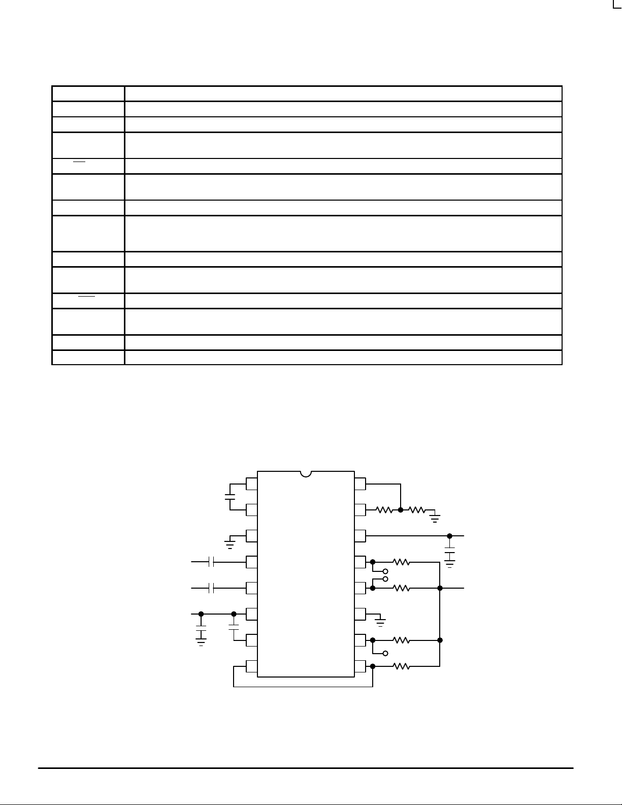
DATA IN
5V
C
bypass
C
AZN
C
AZ
C
AZP
GND
A
C
in
C
in
C
AZ
D
in
D
in
V
CCA
C
LD
Disable LOS
Figure 3. T ypical Operating Circuit
V
V
V
CCE
D
D
GND
LOS
set
ref
out
out
161
R1 R2
152
143
134
125
116
E
107
98
50
DATA OUT
50
50
LEVEL
DETECT OUT
50
5V
C
bypass
3V
MOTOROLA ECLinPS and ECLinPS Lite
2
DL140 — Rev 3

MC10SX1126
Coupling Capacitors
The SX1126 inputs must be AC coupled to allow proper
operation of the offset correction function. The coupling
capacitors, Cin, must be large enough to pass the lowest
input frequency of interest.
Cin+
1
2p(Rin)(f
low
)
where Rin= input resistance = 5000Ω
f
= lowest frequency.
low
Auto–zero Capacitors
A feedback amplifier is used to cancel the offset voltage of
the forward signal path, so the input to the internal ECL
comparator is at its toggle point in the absence of any input
signal. The time constant of the cancelling circuitry is set by
an external capacitor (CAZ) connected between Pins 1 and 2.
The formula for the calculation of the auto–zero capacitor is:
CAZ+
150
2p(RAZ)(f
low
)
where RAZ= internal driving impedance = 290kΩ
f
= lowest frequency.
low
Input Signal Level Detector
The SX1126 allows for user programmable input signal
level–detection and can automatically disable the switching
of its ECL data output if the input level is below a set
threshold. This prevents the outputs from reacting to noise in
the absence of a valid input signal, and ensures that data will
only be transmitted when the signal–to–noise ratio is
sufficient for low bit–error–rate system operation.
Complimentary ECL flags (LOS and LOSB) indicate whether
the input signal is above or below the desired threshold level.
In the level detect system, the input signal is amplified and
rectified before being compared to a programmable
reference. A filter is included to prevent noise spikes from
triggering the level–detector. The filter has a nominal 1µs
time constant, and additional filtering can be achieved by
using an external capacitor (CLD) from Pin 7 to V
CCA
(the
internal driving impedance is nominally 28k). The formula for
the calculation of the CLD capacitor is:
CLD+
t
R
Z
where RZ= internal driving impedance = 28kΩ
t = LOS filter time constant.
DC CHARACTERISTICS (GNDA = GNDE = Ground; V
Symbol Characteristic Min Typ Max Unit Condition
V
IN
V
OS
V
N
V
TH
V
HYS
I
IH
I
CC
1. This device functions with Vinmin = 6mV
2. This device has an anomoly in V
35
30
25
20
(mVpp)
IN
15
V
10
5
0
0.3 0.4 0.5 0.6 0.7 0.8 0.9 1.0 1.1 1.2 1.3 1.4
Input Signal Voltage (Din) Single-Ended 0.008 1.5 V
Input Offset Voltage 50 µV
Input RMS Noise 225 µV
Input Level Detect Programmability 8.0 20 mV
Level Detect Hysteresis 1.5 2.5 7.0 dB Note 2.
Input HIGH Current Disable 150 µA
Power Supply Current 33 45 mA
, but with increased BER (See BER data).
P–P
when 0.65 < V
Input detect
level (LOS 1
Vset (V)
→
HYS
0)
SET
Figure 4. LOS versus Vset (TA = 25°C)
= V
CCA
< 0.75V . Operation in this region is not recommended. (See Figure 5)
= 4.5V to 5.5V)
CCE
8
7
6
5
(dB)
4
HYS
V
3
2
1
0
0.3 0.4 0.5 0.6 0.7 0.8 0.9 1.0 1.1 1.2 1.3 1.4
P-P
P-P
Vset (V)
Note 1.
Figure 5. LOS Hysteresis (TA = 25°C)
ECLinPS and ECLinPS Lite
DL140 — Rev 3
3 MOTOROLA

MC10SX1126
I/O DC CHARACTERISTICS (Note 3.)
–40°C 0°C 25°C 85°C
Symbol Characteristic Min Max Min Max Min Max Min Max Unit
V
OH
V
OL
V
IH
V
IL
I
IL
3. 10SX circuits are designed to meet the DC specifications shown in the table after thermal equilibrium has been established. The circuit is in
a test socket or mounted on a printed circuit board and transverse airflow greater than 500lfpm is maintained. Outputs are terminated through
a 50Ω resistor to –2.0 volts except where otherwise specified on the individual data sheets.
4. Limits hold for VCC = 5.0V only. Parametric values will vary 1:1 with any variation of VCC.
5. Parametric values for the Disable input only.
Output HIGH Voltage
Output LOW Voltage
Input HIGH Voltage (Note 5.)
Input LOW Voltage (Note 5.)
Input LOW Current (Note 5.) 0.5 0.5 0.5 0.3 µA
VCC = –4.5 to –5.5V
VCC = 5.0V (Note 4.)
VCC = –4.5 to –5.5V
VCC = 5.0V (Note 4.)
VCC = –4.5 to –5.5V
VCC = 5.0V (Note 4.)
VCC = –4.5 to –5.5V
VCC = 5.0V (Note 4.)
1080
3920
–1950
3050
–1230
3770
–1950
3050
–890
4110
–1650
3350
–890
4110
–1500
3500
1020
3980
–1950
3050
–1170
3830
–1950
3050
–840
4160
–1630
3370
–840
4160
–1480
3520
–980
4020
–1950
3050
–1130
3870
–1950
3050
–810
4190
–1630
3370
–810
4190
–1480
3520
–910
4090
–1950
3050
–1060
3940
–1950
3050
–720
4280
–1595
3405
–720
4280
–1445
3555
mV
mV
mV
mV
AC CHARACTERISTICS (V
Symbol Characteristic Min Typ Max Unit Condition
BW
BW
t
PWD
tr, t
R
AZ
R
F
t
LD
min
max
f
Lower –3dB Bandwidth 100 MBPS
Upper –3dB Bandwidth 1.25 GBPS
Pulse Width Distortion 70 ps
Rise/Fall Times 150 250 650 ps 20% – 80%
Auto-Zero Output Resistance 200 325 450 kΩ
Level Detect Filter Resistance 14 25 41 kΩ
Level Detect Time Constant 0.5 4.0 µs
CCA
= V
= 4.5V to 5.5V)
CCE
MOTOROLA ECLinPS and ECLinPS Lite
4
DL140 — Rev 3

OUTLINE DIMENSIONS
D SUFFIX
PLASTIC SOIC PACKAGE
CASE 751B–05
ISSUE J
MC10SX1126
-T-
SEATING
PLANE
-A-
916
-B-
1
8
8 PL
P
0.25 (0.010) B
M M
NOTES:
1. DIMENSIONING AND TOLERANCING PER ANSI
Y14.5M, 1982.
2. CONTROLLING DIMENSION: MILLIMETER.
3. DIMENSION A AND B DO NOT INCLUDE MOLD
PROTRUSION.
4. MAXIMUM MOLD PROTRUSION 0.15 (0.006)
PER SIDE.
5. DIMENSION D DOES NOT INCLUDE DAMBAR
PROTRUSION. ALLOWABLE DAMBAR
PROTRUSION SHALL BE 0.127 (0.005) TOTAL
IN EXCESS OF THE D DIMENSION AT
MAXIMUM MATERIAL CONDITION.
G
MILLIMETERS INCHES
MIN MINMAX MAX
DIM
A
9.80
B
3.80
C
1.35
D
0.35
F
0.40
1.27 BSC 0.050 BSC
G
J
0.19
K
0.10
M
0
°
P
5.80
R
0.25
10.00
4.00
1.75
0.49
1.25
0.25
0.25
7
6.20
0.50
0.386
0.393
0.150
0.157
0.054
0.068
0.014
0.019
0.016
0.049
0.008
0.009
0.004
0.009
0
7
°
°
°
0.229
0.010
0.244
0.019
D
16 PL
0.25 (0.010) T B A
M
K
C
S S
R X 45°
M
F
J
Motorola reserves the right to make changes without further notice to any products herein. Motorola makes no warranty, representation or guarantee regarding
the suitability of its products for any particular purpose, nor does Motorola assume any liability arising out of the application or use of any product or circuit, and
specifically disclaims any and all liability, including without limitation consequential or incidental damages. “T ypical” parameters which may be provided in Motorola
data sheets and/or specifications can and do vary in different applications and actual performance may vary over time. All operating parameters, including “Typicals”
must be validated for each customer application by customer’s technical experts. Motorola does not convey any license under its patent rights nor the rights of
others. Motorola products are not designed, intended, or authorized for use as components in systems intended for surgical implant into the body, or other
applications intended to support or sustain life, or for any other application in which the failure of the Motorola product could create a situation where personal injury
or death may occur. Should Buyer purchase or use Motorola products for any such unintended or unauthorized application, Buyer shall indemnify and hold Motorola
and its officers, employees, subsidiaries, affiliates, and distributors harmless against all claims, costs, damages, and expenses, and reasonable attorney fees
arising out of, directly or indirectly, any claim of personal injury or death associated with such unintended or unauthorized use, even if such claim alleges that
Motorola was negligent regarding the design or manufacture of the part. Motorola and are registered trademarks of Motorola, Inc. Motorola, Inc. is an Equal
Opportunity/Affirmative Action Employer.
Mfax is a trademark of Motorola, Inc.
How to reach us:
USA/EUROPE/Locations Not Listed: Motorola Literature Distribution; JAPAN: Nippon Motorola Ltd.: SPD, Strategic Planning Office, 141,
P.O. Box 5405, Denver, Colorado 80217. 1–303–675–2140 or 1–800–441–2447 4–32–1 Nishi–Gotanda, Shagawa–ku, Tokyo, Japan. 03–5487–8488
Customer Focus Center: 1–800–521–6274
Mfax: RMFAX0@email.sps.mot.com – TOUCHTONE 1–602–244–6609 ASIA/P ACIFIC: Motorola Semiconductors H.K. Ltd.; 8B Tai Ping Industrial Park,
Moto rola Fax Back System – US & Canada ONLY 1–800–774–1848 51 Ting Kok Road, Tai Po, N.T., Hong Kong. 852–26629298
– http://sps.motorola.com/mfax/
HOME PAGE: http://motorola.com/sps/
MC10SX1126/D
ECLinPS and ECLinPS Lite
◊
5 MOTOROLA
DL140 — Rev 3
 Loading...