

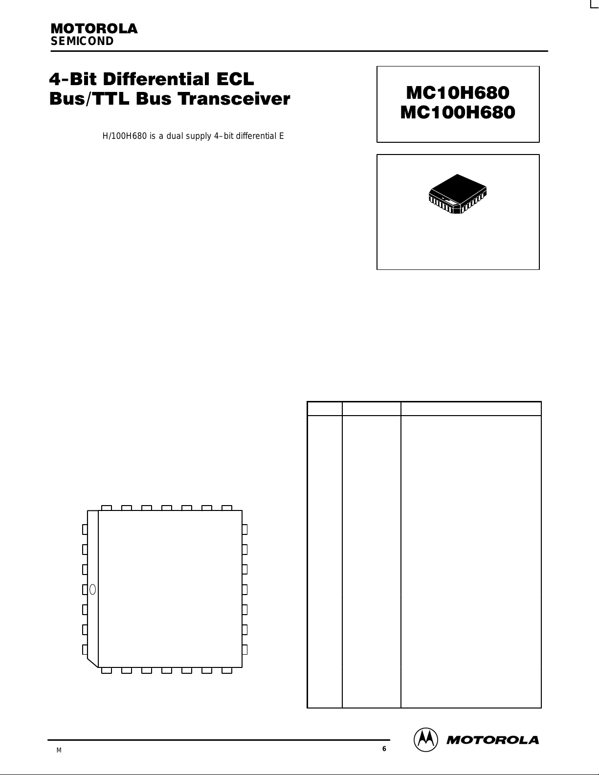
SEMICONDUCTOR TECHNICAL DATA
The MC10H/100H680 is a dual supply 4–bit differential ECL bus to TTL
bus transceiver. It is designed to allow the system designer to no longer be
limited in bus speed associated with standard TTL busses. Using a
differential ECL Bus will increase the frequency of operation and increase
noise immunity .
Both the TTL and the ECL ports are capable of driving a bus. The ECL
outputs have the ability to drive 25 Ω, allowing both ends of the bus line to be
terminated in the characteristic impedance of 50 Ω. The TTL outputs are
specified to source 15 mA and sink 48 mA, allowing the ability to drive highly
capacitive loads.
The ECL output levels are VOH approximately equal to –1.0 V and V
cutoff equal to –2.0 V (VTT). When the ECL ports are disabled both EIOx and
EIOxB go to the VOL cutoff level. The ECL input receivers have special
circuitry which detects this disabled condition, prevents oscillation, and
forces the TTL output to the low state. The noise margin in this disabled state
is greater than 600 mV. Multiple ECL V
pins are utilized to minimize
CCO
switching noise.
The TTL ports have standard levels. The TTL input receivers have PNP
input devices to significantly reduce loading. Multiple TTL power and ground
pins are utilized to minimize switching noise.
The control pins (EDIR and ECEB) of the 10H version is compatible with
MECL 10H ECL logic levels. The control pins of the 100H version are
compatible with 100K levels.
OL
FN SUFFIX
PLASTIC PACKAGE
CASE 776–02
• Differential ECL Bus (25 Ω) I/O Ports
• High Drive TTL Bus I/O Ports
• Extra TTL and ECL Power/Ground Pins to Minimize
Switching Noise
• Dual Supply
• Direction and Chip Enable Control Pins
Pinout: 28–Lead PLCC (Top View)
TIO2
GT3
VT2
25 24 23 22 21 20 19
T101
26
27
GT2
28
VT1
1
GT1
2
TIO0
3
TDIR
412
EDIR
567891011
EIO0
CCO1
EIO0B
V
GT4
EE
V
TIO3
EI01
TCEB
CCO2
V
ECEB
18
17
16
15
14
13
EIO1B
EIO3B
V
EIO3
V
EIO2B
V
EIO2
CCO4
CCE
CCO3
PIN DESCRIPTIONS
Pin Symbol Function
1 GT1 TTL Ground 1
2 TIO0 TTL I/O Bit 0
3 TDIR TTL Direction Control
4 EDIR ECL Direction Control
5 EIO0 ECL I/O Bit 0
6 VCCO1 ECL VCC 1 (0V) – Outputs
7 EIO0B ECL I/O Bit 0 Bar
8 VEE ECL Supply (–5.2/–4.5V)
9 EIO1 ECL I/O Bit 1
10 VCCO2 ECL VCC 2 (0V) – Outputs
11 EIO1B ECL I/O Bit 1 Bar
12 EIO2 ECL I/O Bit 2
13 VCCO3 ECL VCC 3 (0V) – Outputs
14 EIO2B ECL I/O Bit 2 Bar
15 VCCE ECL VCC (0V)
16 EIO3 ECL I/O Bit 3
17 VCCO4 ECL VCC 4 (0V) – Outputs
18 EIO3B ECL I/O Bit 3 Bar
19 ECEB ECL Chip Enable Bar Control
20 TCEB TTL Chip Enable Bar Control
21 TIO3 TTL I/O Bit 3
22 GT4 TTL Ground 4
23 VT2 TTL Supply 2 (5V)
24 GT3 TTL Ground 3
25 TIO2 TTL I/O Bit 2
26 TIO1 TTL I/O Bit 1
27 GT2 TTL Ground 2
28 VT1 TTL Supply 1 (5V)
9/96
Motorola, Inc. 1996
2–144
REV 6
TRUTH TABLE
MC10H680 MC100H680
TDIR — Direction Control TTL Levels
EDIR — Direction Control ECL Levels
TCEB — Chip Enable Bar Control TTL Levels
ECEB — Chip Enable Bar Control ECL Levels
TIN — TTL Input
TOUT — TTL Output
EIN — ECL Input
EINB — ECL Input Bar
EOUT — ECL Output
EOUTB — ECL Output Bar
ECEB
TCEB EDIR TDIR EIN EINB EOUT EOUTB TIN TOUT COMMENTS
H X X X X X LC LC X Z ECL and TTL Outputs Disabled
X H X X X X LC LC X Z ECL and TTL Outputs Disabled
L L H X H LC NA H ECL to TTL Direction
L L H X LC H NA L ECL to TTL Direction
L L H X LC LC NA L ECL to TTL Direction (L–L Cond.)
L L X H H LC NA H ECL to TTL Direction
L L X H LC H NA L ECL to TTL Direction
L L X H LC LC NA L ECL to TTL Direction (L–L Cond.)
L L L L NA NA H LC H TTL to ECL Direction
L L L L NA NA LC H L TTL to ECL Direction
H — HIGH
L — LOW
LC — ECL Low Cutoff (VTT = –2.0 V)
X — Don’t Care
Z — High Impedance
ABSOLUTE RATINGS (Do not exceed):
Power Supply Voltage VEE (ECL) –8.0 to 0 Vdc
Power Supply Voltage V
Input Voltage VI (ECL)
Disabled 3–State Output V
Output Source Current Continuous I
Output Source Current Surge I
Storage Temperature T
Operating Temperature T
(TTL) –0.5 to +7.0 Vdc
CCT
0.0 to V
VI (TTL)
(TTL) 0.0 to V
out
(ECL) 100 mAdc
out
(ECL) 200 mAdc
out
stg
amb
EE
–0.5 to +7.0
CCT
–65 to 150 °C
0.0 to +75 °C
Vdc
Vdc
DL122 — Rev 6
2–145 MOTOROLAMECL Data
MC10H680 MC100H680
Test
Test
Test
Test
Test
ECL DC CHARACTERISTICS: V
Test
Symbol
I
EE
I
INH
I
INL
V
OH
V
OL
Supply Current/ECL –110 –110 –110 mA
Input HIGH Current 225 145 145 µA
Input LOW Current 0.5 0.5 0.3 µA
Output HIGH Voltage
Output LOW Voltage
Parameter Min Max Min Max Min Max Unit Condition
CCT
CONTROL INPUTS ONLY
10H ECL DC CHARACTERISTICS:
Test
Symbol
V
IH
V
IL
Input HIGH Voltage
Input LOW Voltage
Parameter Min Max Min Max Min Max Unit Condition
CONTROL INPUTS ONLY
100H ECL DC CHARACTERISTICS:
Test
Symbol
V
IH
V
IL
Input HIGH Voltage
Input LOW Voltage
Parameter Min Max Min Max Min Max Unit Condition
= +5.0 V ±10%, VEE = –5.2 ±5% (10H Version); VEE = –4.2 V to –5.5 V (100H Version)
TA = 0°C TA = 25°C TA = 75°C
–1100
–2.1
V
= +5.0 ±10%, VEE = –5.2 ±5%
CCT
–1170
–1950
V
= +5.0 ±10%, VEE = –4.2 V to –5.5 V
CCT
–1165
–1810
–840
–2.03
TA = 0°C TA = 25°C TA = 75°C
–840
–1480
TA = 0°C TA = 25°C TA = 75°C
–880
–1475
–1100
–2.1
–1130
–1950
–1165
–1810
–810
–2.03
–810
–1480
–880
–1475
–1100
–2.1
–1070
–1950
–1165
–1810
–735
–1450
–880
–1475
–735
–2.03
mVV25 Ω to –2.1 V
mV
mV
TTL DC CHARACTERISTICS: V
Test
Symbol
V
IH
V
IL
V
IK
V
OH
V
OL
IIH* TTL (Input HIGH)
IIL* TTL (Input LOW) –0.6 –0.6 –0.6 mA Vin = 0.5 V
I
CCL
I
CCH
I
CCZ
I
OS
* NOTE: TTL Control Inputs only
Standard Input
Standard Input
Input Clamp –1.2 –1.2 –1.2 Vdc IIN = –18 mA
Output HIGH Voltage
Output HIGH Voltage
Output LOW Voltage 0.55 0.55 0.55 V IOL = 48 mA
TTL (Input HIGH)
Supply Current 75 75 75 mA
Supply Current 70 70 70 mA
Supply Current 70 70 70 mA
Output Short Circuit Current –100 –225 –100 –225 –100 –225 mA V
Parameter Min Max Min Max Min Max Unit Condition
= +5.0 V ±10%, VEE = –5.2 ±5% (10H Version); VEE = –4.2 V to –5.5 V (100H Version)
CCT
TA = 0°C TA = 25°C TA = 75°C
2.0
0.8
2.5
2.0
20
100
2.0
2.5
2.0
0.8
20
100
2.0
2.5
2.0
0.8
20
100
Vdc
V IOH = –3.0 mA
µA Vin = 2.7 V
IOH = –15 mA
Vin = 7.0 V
OUT
TTL I/O DC CHARACTERISTICS ONLY
Test
Symbol
I
IH/IOZH
I
IL/IOZL
Parameter Min Max Min Max Min Max Unit Condition
Output Disable
Current
TA = 0°C TA = 25°C TA = 75°C
70
200
70
200
70
200
µA V
V
OUT
OUT
= 0 V
= 2.7 V
= 0.5 V
MOTOROLA MECL Data
2–146
DL122 — Rev 6

ECL TO TTL DIRECTION / AC TEST
Test
Test
Test
Symbol
t
PLH
t
PHL
t
PZH
t
PZL
t
PHZ
t
PLZ
t
PZH
t
PZL
t
PHZ
t
PLZ
tr/t
f
Parameter Waveforms Min Max Min Max Min Max Unit Condition
Propagation Delay
to Output
ECEB to Output
Enable Time
ECEB to Output
Disable Time
TCEB to Output
Enable Time
TCEB to Output
Disable Time
1.0 to 2.0 Vdc 3 0.4 1.5 0.4 1.5 0.4 1.5 ns CL = 50 pF
TTL TO ECL DIRECTION / AC TEST
Test
Symbol
t
PLH
t
PHL
t
PLH
t
PHL
t
PLH
t
PHL
tr/t
f
Parameter Waveforms Min Max Min Max Min Max Unit Condition
Propagation Delay
to Output
ECEB
to Output
TCEB
to Output
Output Rise/Fall
Time 20%–80%
MC10H680 MC100H680
TA = 0°C TA = 25°C TA = 75°C
2, 4 2.7 4.8 2.7 4.8 2.7 4.8 ns CL = 50 pF
2, 5, 6 3.5
3.5
2, 5, 6 3.5
3.5
2, 5, 6 5.7
5.4
2, 5, 6 4.0
4.0
1, 4 1.8 4.6 1.8 4.6 2.0 4.9 ns 25 Ω to –2.0 V
1, 4 2.9 5.1 3.0 5.2 3.4 5.7 ns 25 Ω to –2.0 V
1, 4 3.4 6.3 3.5 6.6 3.8 7.4 ns 25 Ω to –2.0 V
1, 3 1.0 3.4 1.0 3.4 1.0 3.4 ns 25 Ω to –2.0 V
6.5
6.0
8.6
6.5
7.7
6.9
8.5
5.8
TA = 0°C TA = 25°C TA = 75°C
3.5
3.5
3.5
3.5
5.7
5.4
4.1
4.2
6.5
6.0
8.6
6.5
7.7
6.9
8.4
6.0
3.7
3.7
3.7
3.7
5.9
5.9
4.2
4.7
6.7
6.4
8.8
7.3
7.9
7.4
8.3
6.5
ns CL = 50 pF
ns CL = 50 pF
ns CL = 50 pF
ns CL = 50 pF
DL122 — Rev 6
2–147 MOTOROLAMECL Data

MC10H680 MC100H680
CONTROL INPUTS
TDIR
EDIR
TCE
ECE
BLOCK DIAGRAM
EOE
TOE
V
CCE
V
EE
V
CCT1
GND1
TIO0
GND2
TIO1
GND3
V
CCO1
EIO0
EIO0
V
CCO2
EIO1
EIO1
V
CCO3
ECL I/OTTL I/O
TIO2
V
CCT2
GND4 V
TIO3
MOTOROLA MECL Data
2–148
EIO2
EIO2
CCO4
EIO3
EIO3
DL122 — Rev 6

SWITCHING CIRCUIT AND WAVEFORMS
MC10H680 MC100H680
PULSE
GENERAT OR
ECL/TTL
ECL
USE 0.1 µF CAPACIT ORS
FOR DECOUPLING.
50 Ω COAX
USE OSCILLOSCOPE
INTERNAL 50
FOR TERMINATION.
Ω
LOAD
Figure 1. Switching Circuit ECL
V
EE
IN OUT
Ω
COAX50
CH A
OSCILLOSCOPE
VCC & V
DEVICE
UNDER
TEST
CCO
CH B
50
Ω
Ω
COAX50
ECL/TTL
TTL
DEVICE
UNDER
TEST
t
, t
PZL
PLZ
O,C
50 pF
Figure 2.
+7 V OPEN
R1
500
R2
500
ALL
OTHERS
Ω
Ω
V
OUT
T
RISE
T
FALL
Figure 3. WAVEFORMS: Rise and Fall Times
TTL
VE
VE
V
OUT
1.5 V
1.5 V
T
PZL
1.5 V
80%/2.0 V
T
PLZ
0.3 V
20%/1.0 V
V
OL
50%/1.5 V
V
V
OUT
IN
T
PD++
50%/1.5 V
T
PLH
T
Figure 4. Propagation Delay — Single Ended
TTL
VE
1.5 V
VE
T
PZH
V
OUT
1.5 V
T
PHL
PD––
1.5 V
T
PHZ
0.3 V
>
VOH
3.5 V
≈
Figure 5. 3–State Output Low Enable and Disable
Times
DL122 — Rev 6
Figure 6. 3–State Output High Enable and Disable
Times
2–149 MOTOROLAMECL Data

MC10H680 MC100H680
OUTLINE DIMENSIONS
FN SUFFIX
PLASTIC PLCC PACKAGE
CASE 776–02
ISSUE D
–L–
–N–
28 1
Z
C
G
G1
S
0.010 (0.250) N
L–M
T
S
L–M
T
M
S
S
L–M
T
S
Y BRK
0.007 (0.180) N
B
0.007 (0.180) N
U
M
D
Z
–M–
W
D
V
0.010 (0.250) N
G1X
S
S
L–M
T
S
VIEW D–D
A
0.007 (0.180) N
0.007 (0.180) N
R
E
M
M
S
L–M
T
L–M
T
S
S
S
H
0.007 (0.180) N
M
S
L–M
T
S
K1
0.004 (0.100)
SEATING
J
–T–
PLANE
VIEW S
S
S
K
VIEW S
0.007 (0.180) N
F
M
S
L–M
T
S
NOTES:
1. DATUMS –L–, –M–, AND –N– DETERMINED
WHERE TOP OF LEAD SHOULDER EXITS
PLASTIC BODY AT MOLD PARTING LINE.
2. DIMENSION G1, TRUE POSITION TO BE
MEASURED AT DA TUM –T–, SEATING PLANE.
3. DIMENSIONS R AND U DO NOT INCLUDE
MOLD FLASH. ALLOWABLE MOLD FLASH IS
0.010 (0.250) PER SIDE.
4. DIMENSIONING AND TOLERANCING PER
ANSI Y14.5M, 1982.
5. CONTROLLING DIMENSION: INCH.
6. THE PACKAGE TOP MAY BE SMALLER THAN
THE PACKAGE BOTTOM BY UP TO 0.012
(0.300). DIMENSIONS R AND U ARE
DETERMINED AT THE OUTERMOST
EXTREMES OF THE PLASTIC BODY
EXCLUSIVE OF MOLD FLASH, TIE BAR
BURRS, GATE BURRS AND INTERLEAD
FLASH, BUT INCLUDING ANY MISMATCH
BETWEEN THE TOP AND BOTTOM OF THE
PLASTIC BODY.
7. DIMENSION H DOES NOT INCLUDE DAMBAR
PROTRUSION OR INTRUSION. THE DAMBAR
PROTRUSION(S) SHALL NOT CAUSE THE H
DIMENSION TO BE GREATER THAN 0.037
(0.940). THE DAMBAR INTRUSION(S) SHALL
NOT CAUSE THE H DIMENSION TO BE
SMALLER THAN 0.025 (0.635).
DIM MIN MAX MIN MAX
A 0.485 0.495 12.32 12.57
B 0.485 0.495 12.32 12.57
C 0.165 0.180 4.20 4.57
E 0.090 0.110 2.29 2.79
F 0.013 0.019 0.33 0.48
G 0.050 BSC 1.27 BSC
H 0.026 0.032 0.66 0.81
J 0.020 ––– 0.51 –––
K 0.025 ––– 0.64 –––
R 0.450 0.456 11.43 11.58
U 0.450 0.456 11.43 11.58
V 0.042 0.048 1.07 1.21
W 0.042 0.048 1.07 1.21
X 0.042 0.056 1.07 1.42
Y ––– 0.020 ––– 0.50
Z 2 10 2 10
____
G1 0.410 0.430 10.42 10.92
K1 0.040 ––– 1.02 –––
MILLIMETERSINCHES
MOTOROLA MECL Data
2–150
DL122 — Rev 6

MC10H680 MC100H680
Motorola reserves the right to make changes without further notice to any products herein. Motorola makes no warranty , representation or guarantee regarding
the suitability of its products for any particular purpose, nor does Motorola assume any liability arising out of the application or use of any product or circuit, and
specifically disclaims any and all liability, including without limitation consequential or incidental damages. “T ypical” parameters which may be provided in Motorola
data sheets and/or specifications can and do vary in different applications and actual performance may vary over time. All operating parameters, including “Typicals”
must be validated for each customer application by customer’s technical experts. Motorola does not convey any license under its patent rights nor the rights of
others. Motorola products are not designed, intended, or authorized for use as components in systems intended for surgical implant into the body, or other
applications intended to support or sustain life, or for any other application in which the failure of the Motorola product could create a situation where personal injury
or death may occur. Should Buyer purchase or use Motorola products for any such unintended or unauthorized application, Buyer shall indemnify and hold Motorola
and its officers, employees, subsidiaries, affiliates, and distributors harmless against all claims, costs, damages, and expenses, and reasonable attorney fees
arising out of, directly or indirectly, any claim of personal injury or death associated with such unintended or unauthorized use, even if such claim alleges that
Motorola was negligent regarding the design or manufacture of the part. Motorola and are registered trademarks of Motorola, Inc. Motorola, Inc. is an Equal
Opportunity/Affirmative Action Employer.
How to reach us:
USA/EUROPE/Locations Not Listed: Motorola Literature Distribution; JAPAN: Nippon Motorola Ltd.; Tatsumi–SPD–JLDC, 6F Seibu–Butsuryu–Center,
P.O. Box 20912; Phoenix, Arizona 85036. 1–800–441–2447 or 602–303–5454 3–14–2 Tatsumi Koto–Ku, Tokyo 135, Japan. 03–81–3521–8315
MFAX: RMF AX0@email.sps.mot.com – T OUCHTONE 602–244–6609 ASIA/PACIFIC: Motorola Semiconductors H.K. Ltd.; 8B Tai Ping Industrial Park,
INTERNET: http://Design–NET .com 51 Ting Kok Road, Tai Po, N.T., Hong Kong. 852–26629298
MC10H680/D
DL122 — Rev 6
◊
2–151 MOTOROLAMECL Data
*MC10H680/D*
 Loading...