

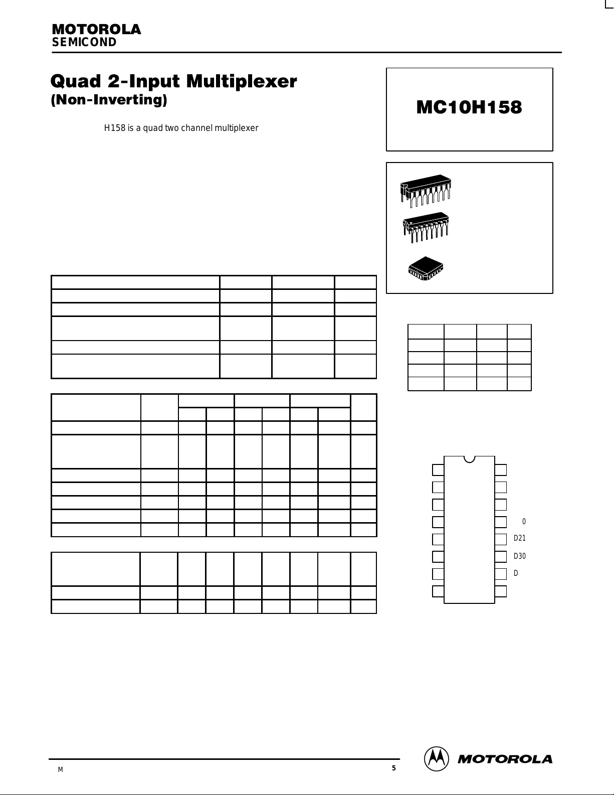
SEMICONDUCTOR TECHNICAL DATA
"
!
The MC10H158 is a quad two channel multiplexer with common input select.
A “high” level select enables input D00, D10, D20 and D30 and a “low” level
select enables input D01, D11, D21 and D31. This MECL 10H part is a
functional/pinout duplication of the standard MECL 10K family part, with 100%
improvement in propagation delay and no increase in power–supply current.
• Propagation Delay, 1.5 ns Typical
• Power Dissipation, 197 mW Typical
• Improved Noise Margin 150 mV (Over Operating Voltage and
Temperature Range)
• Voltage Compensated
• MECL 10K–Compatible
MAXIMUM RATINGS
Characteristic Symbol Rating Unit
Power Supply (VCC = 0) V
Input Voltage (VCC = 0) V
Output Current— Continuous
— Surge
Operating Temperature Range T
Storage Temperature Range— Plastic
— Ceramic
T
I
EE
I
out
A
stg
ELECTRICAL CHARACTERISTICS (VEE = –5.2 V ±5%)
0° 25° 75°
Characteristic Symbol Min Max Min Max Min Max Unit
Power Supply Current I
Input Current High
Pin 9
Pins 3–6 and 10–13
Input Current Low I
High Output Voltage V
Low Output Voltage V
High Input Voltage V
Low Input Voltage V
I
E
inH
inL
OH
OL
IH
— 53 — 48 — 53 mA
——475
515——
0.5 — 0.5 — 0.3 — µA
–1.02 –0.84 –0.98 –0.81 –0.92 –0.735 Vdc
–1.95 –1.63 –1.95 –1.63 –1.95 –1.60 Vdc
–1.17 –0.84 –1.13 –0.81 –1.07 –0.735 Vdc
–1.95 –1.48 –1.95 –1.48 –1.95 –1.45 Vdc
IL
AC PARAMETERS
Propagation Delay
Data
Select
Rise Time t
Fall Time t
NOTE:
Each MECL 10H series circuit has been designed to meet the dc specifications shown in the test table,
after thermal equilibrium has been established. The circuit is in a test socket or mounted on a printed circuit
board and transverse air flow greater than 500 Iinear fpm is maintained. Outputs are terminated through
a 50–ohm resistor to –2.0 volts.
t
pd
0.5
1.9
2.9
0.5
1.0
1.0
0.7 2.2 0.7 2.2 0.7 2.2 ns
r
0.7 2.2 0.7 2.2 0.7 2.2 ns
f
–8.0 to 0 Vdc
0 to V
EE
50
100
0 to +75 °C
–55 to +150
–55 to +165
295
320——
1.9
0.5
2.9
1.0
Vdc
mA
°C
°C
295
320
2.0
2.9
µA
ns
L SUFFIX
CERAMIC PACKAGE
CASE 620–10
P SUFFIX
PLASTIC PACKAGE
CASE 648–08
FN SUFFIX
PLCC
CASE 775–02
TRUTH TABLE
Select D0 D1 Q
LLLX
LHHX
HXLL
HXHH
DIP
PIN ASSIGNMENT
Q0
Q1
D11
D10
D01
D00
NC
V
EE
Pin assignment is for Dual–in–Line Package.
For PLCC pin assignment, see the Pin Conversion
T ables on page 6–11 of the Motorola MECL Data
1
2
3
4
5
6
7
8
Book (DL122/D).
16
15
14
13
12
11
10
V
CC
Q2
Q3
D20
D21
D30
D31
SELECT
9
3/93
Motorola, Inc. 1996
2–238
REV 5
SELECT 9
MC10H158
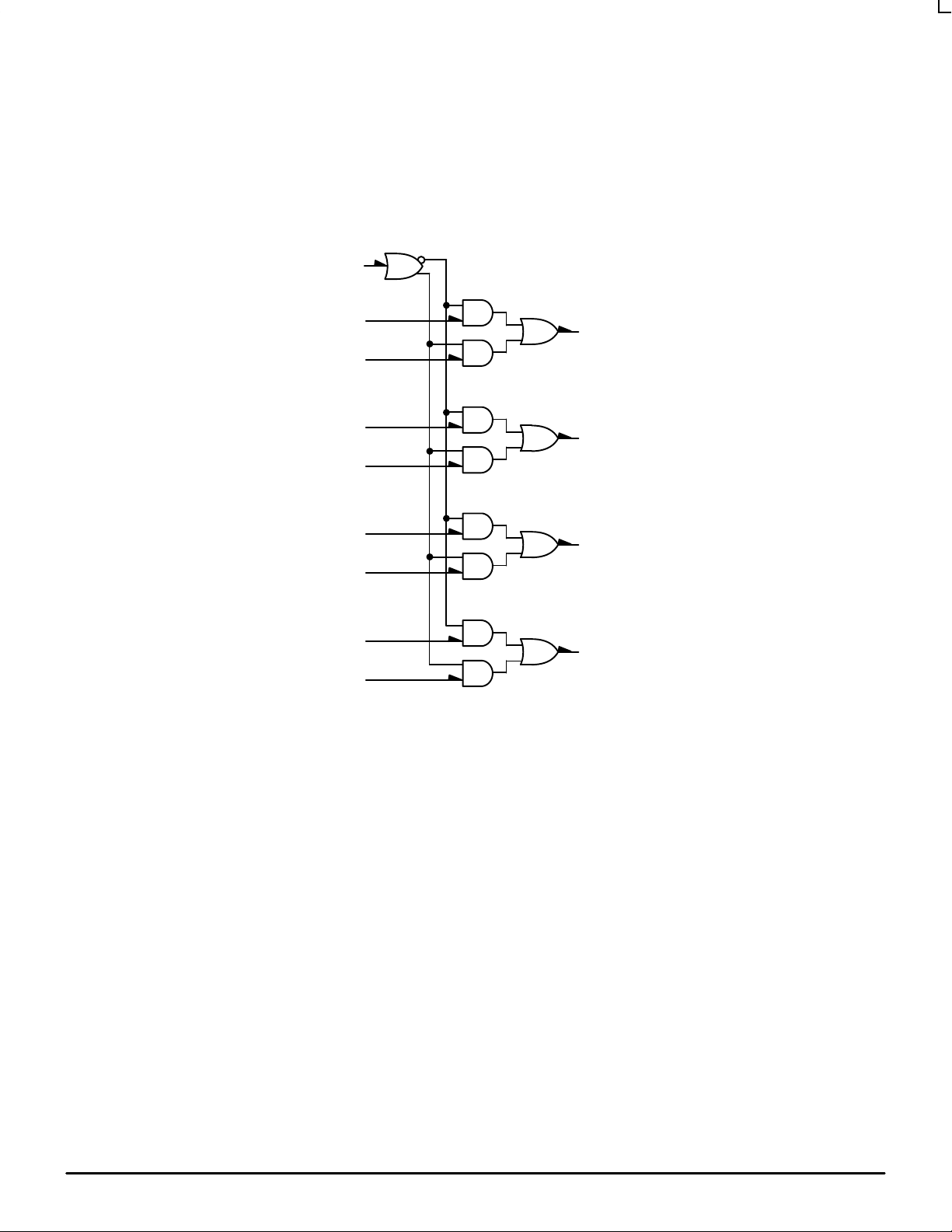
LOGIC DIAGRAM
D0 1 5
D0 0 6
D1 1 3
D1 0 4
D2 1 12
D2 0 13
D3 1 10
D3 0 11
1 Q0
2 Q1
15 Q2
14 Q3
VCC = PIN 16
VEE = PIN 8
DL122 — Rev 6
2–239 MOTOROLAMECL Data
MC10H158
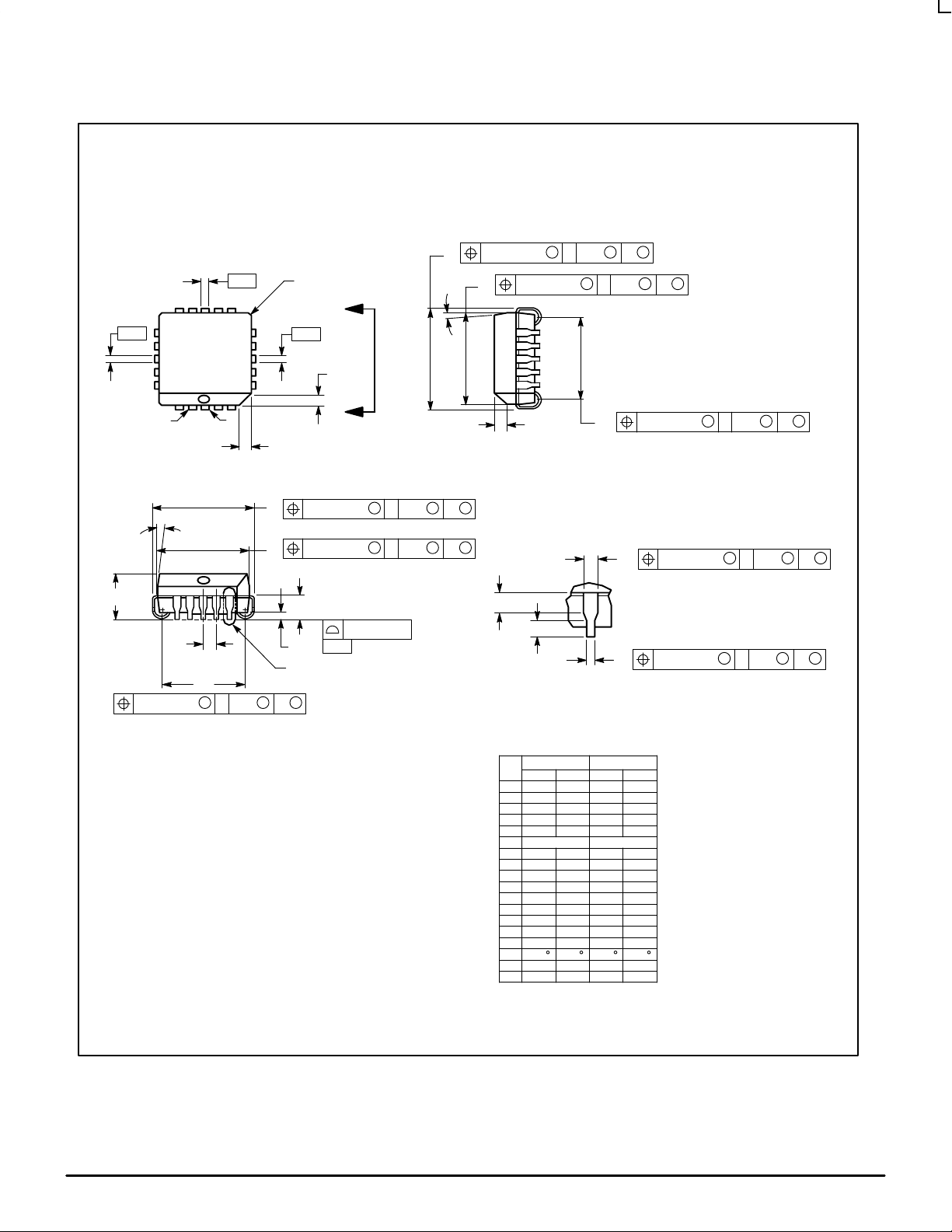
OUTLINE DIMENSIONS
FN SUFFIX
PLASTIC PLCC PACKAGE
CASE 775–02
ISSUE C
–L–
20 1
Z
C
G
G1
0.010 (0.250) N
S
T
–N–
L–M
S
Y BRK
–M–
W
V
A
0.007 (0.180) N
0.007 (0.180) N
R
E
0.004 (0.100)
J
PLANE
SEATING
–T–
VIEW S
S
0.007 (0.180) N
B
0.007 (0.180) N
U
M
S
L–M
T
M
S
S
L–M
T
S
D
Z
D
X
0.010 (0.250) N
G1
S
S
L–M
T
S
VIEW D–D
M
M
S
L–M
T
L–M
T
S
S
S
0.007 (0.180) N
H
M
S
L–M
T
S
K1
K
0.007 (0.180) N
F
M
S
L–M
T
S
VIEW S
NOTES:
1. DATUMS –L–, –M–, AND –N– DETERMINED
WHERE TOP OF LEAD SHOULDER EXITS PLASTIC
BODY AT MOLD PARTING LINE.
2. DIMENSION G1, TRUE POSITION TO BE
MEASURED AT DA TUM –T–, SEATING PLANE.
3. DIMENSIONS R AND U DO NOT INCLUDE MOLD
FLASH. ALLOWABLE MOLD FLASH IS 0.010 (0.250)
PER SIDE.
4. DIMENSIONING AND TOLERANCING PER ANSI
Y14.5M, 1982.
5. CONTROLLING DIMENSION: INCH.
6. THE PACKAGE TOP MAY BE SMALLER THAN THE
PACKAGE BOTTOM BY UP TO 0.012 (0.300).
DIMENSIONS R AND U ARE DETERMINED AT THE
OUTERMOST EXTREMES OF THE PLASTIC BODY
EXCLUSIVE OF MOLD FLASH, TIE BAR BURRS,
GATE BURRS AND INTERLEAD FLASH, BUT
INCLUDING ANY MISMATCH BETWEEN THE TOP
AND BOTTOM OF THE PLASTIC BODY.
7. DIMENSION H DOES NOT INCLUDE DAMBAR
PROTRUSION OR INTRUSION. THE DAMBAR
PROTRUSION(S) SHALL NOT CAUSE THE H
DIMENSION TO BE GREATER THAN 0.037 (0.940).
THE DAMBAR INTRUSION(S) SHALL NOT CAUSE
THE H DIMENSION TO BE SMALLER THAN 0.025
(0.635).
MOTOROLA MECL Data
DIM MIN MAX MIN MAX
A 0.385 0.395 9.78 10.03
B 0.385 0.395 9.78 10.03
C 0.165 0.180 4.20 4.57
E 0.090 0.110 2.29 2.79
F 0.013 0.019 0.33 0.48
G 0.050 BSC 1.27 BSC
H 0.026 0.032 0.66 0.81
J 0.020 ––– 0.51 –––
K 0.025 ––– 0.64 –––
R 0.350 0.356 8.89 9.04
U 0.350 0.356 8.89 9.04
V 0.042 0.048 1.07 1.21
W 0.042 0.048 1.07 1.21
X 0.042 0.056 1.07 1.42
Y ––– 0.020 ––– 0.50
Z 2 10 2 10
____
G1 0.310 0.330 7.88 8.38
K1 0.040 ––– 1.02 –––
2–240
MILLIMETERSINCHES
DL122 — Rev 6

OUTLINE DIMENSIONS
CERAMIC DIP PACKAGE
–A–
16 9
–B–
18
C
–T–
SEATING
PLANE
E
F
G
16 PLD
0.25 (0.010) T
M
–A–
916
B
18
F
C
S
H
G
D
16 PL
0.25 (0.010) T
K
M
K
N
S
A
PLASTIC DIP PACKAGE
SEATING
–T–
PLANE
M
A
L SUFFIX
CASE 620–10
ISSUE V
L
M
16 PLJ
0.25 (0.010) T
P SUFFIX
CASE 648–08
ISSUE R
L
J
MC10H158
NOTES:
1. DIMENSIONING AND TOLERANCING PER
ANSI Y14.5M, 1982.
2. CONTROLLING DIMENSION: INCH.
3. DIMENSION L TO CENTER OF LEAD WHEN
FORMED PARALLEL.
4. DIMENSION F MAY NARROW TO 0.76 (0.030)
WHERE THE LEAD ENTERS THE CERAMIC
BODY.
DIM MIN MAX MIN MAX
A 0.750 0.785 19.05 19.93
B 0.240 0.295 6.10 7.49
C ––– 0.200 ––– 5.08
D 0.015 0.020 0.39 0.50
E 0.050 BSC 1.27 BSC
F 0.055 0.065 1.40 1.65
G 0.100 BSC 2.54 BSC
H 0.008 0.015 0.21 0.38
K 0.125 0.170 3.18 4.31
M
S
B
NOTES:
1. DIMENSIONING AND TOLERANCING PER ANSI
2. CONTROLLING DIMENSION: INCH.
3. DIMENSION L TO CENTER OF LEADS WHEN
4. DIMENSION B DOES NOT INCLUDE MOLD FLASH.
5. ROUNDED CORNERS OPTIONAL.
M
L 0.300 BSC 7.62 BSC
M 0 15 0 15
____
N 0.020 0.040 0.51 1.01
Y14.5M, 1982.
FORMED PARALLEL.
DIM MIN MAX MIN MAX
A 0.740 0.770 18.80 19.55
B 0.250 0.270 6.35 6.85
C 0.145 0.175 3.69 4.44
D 0.015 0.021 0.39 0.53
F 0.040 0.70 1.02 1.77
G 0.100 BSC 2.54 BSC
H 0.050 BSC 1.27 BSC
J 0.008 0.015 0.21 0.38
K 0.110 0.130 2.80 3.30
L 0.295 0.305 7.50 7.74
M 0 10 0 10
S 0.020 0.040 0.51 1.01
MILLIMETERSINCHES
MILLIMETERSINCHES
____
Motorola reserves the right to make changes without further notice to any products herein. Motorola makes no warranty , representation or guarantee regarding
the suitability of its products for any particular purpose, nor does Motorola assume any liability arising out of the application or use of any product or circuit, and
specifically disclaims any and all liability, including without limitation consequential or incidental damages. “T ypical” parameters which may be provided in Motorola
data sheets and/or specifications can and do vary in different applications and actual performance may vary over time. All operating parameters, including “Typicals”
must be validated for each customer application by customer’s technical experts. Motorola does not convey any license under its patent rights nor the rights of
others. Motorola products are not designed, intended, or authorized for use as components in systems intended for surgical implant into the body, or other
applications intended to support or sustain life, or for any other application in which the failure of the Motorola product could create a situation where personal injury
or death may occur. Should Buyer purchase or use Motorola products for any such unintended or unauthorized application, Buyer shall indemnify and hold Motorola
and its officers, employees, subsidiaries, affiliates, and distributors harmless against all claims, costs, damages, and expenses, and reasonable attorney fees
arising out of, directly or indirectly, any claim of personal injury or death associated with such unintended or unauthorized use, even if such claim alleges that
Motorola was negligent regarding the design or manufacture of the part. Motorola and are registered trademarks of Motorola, Inc. Motorola, Inc. is an Equal
Opportunity/Affirmative Action Employer.
How to reach us:
USA/EUROPE/Locations Not Listed: Motorola Literature Distribution; JAPAN: Nippon Motorola Ltd.; Tatsumi–SPD–JLDC, 6F Seibu–Butsuryu–Center,
P.O. Box 20912; Phoenix, Arizona 85036. 1–800–441–2447 or 602–303–5454 3–14–2 Tatsumi Koto–Ku, Tokyo 135, Japan. 03–81–3521–8315
MFAX: RMF AX0@email.sps.mot.com – T OUCHTONE 602–244–6609 ASIA/P ACIFIC: Motorola Semiconductors H.K. Ltd.; 8B Tai Ping Industrial Park,
INTERNET: http://Design–NET .com 51 Ting Kok Road, Tai Po, N.T., Hong Kong. 852–26629298
MC10H158/D
DL122 — Rev 6
◊
2–241 MOTOROLAMECL Data
*MC10H158/D*
 Loading...