

MOTOROLA MC10H116DR2, MC10H116FNR2, MC10H116M, MC10H116MEL, MC10H116ML1 Datasheet
...
SEMICONDUCTOR TECHNICAL DATA
2–219
REV 6
Motorola, Inc. 1996
9/96
The MC10H116 is a functional/pinout duplication of the MC10116, with 100%
improvement in propagation delay and no increase in power– supply current.
• Propagation Delay, 1.0 ns Typical
• Power Dissipation 85 mW Typ/Pkg (same as MECL 10K)
• Improved Noise Margin 150 mV (Over Operating Voltage and
Temperature Range)
• Voltage Compensated
• MECL 10K–Compatible
MAXIMUM RATINGS
Characteristic Symbol Rating Unit
Power Supply (VCC = 0) V
EE
–8.0 to 0 Vdc
Input Voltage (VCC = 0) V
I
0 to V
EE
Vdc
Output Current — Continuous
— Surge
I
out
50
100
mA
Operating T emperature Range T
A
0 to +75 °C
Storage T emperature Range — Plastic
— Ceramic
T
stg
–55 to +150
–55 to +165
°C
°C
ELECTRICAL CHARACTERISTICS (VEE = –5.2 V ±5%) (2)
0° 25° 75°
Characteristic Symbol Min Max Min Max Min Max Unit
Power Supply Current I
E
— 23 — 21 — 23 mA
Input Current High I
inH
— 150 — 95 — 95 µA
Input Leakage Current I
CBO
— 1.5 — 1.0 — 1.0 µA
Reference Voltage V
BB
–1.38 –1.27 –1.35 –1.25 –1.31 –1.19 Vdc
High Output Voltage V
OH
–1.02 –0.84 –0.98 –0.81 –0.92 –0.735 Vdc
Low Output Voltage V
OL
–1.95 –1.63 –1.95 –1.63 –1.95 –1.60 Vdc
High Input Voltage (1) V
IH
–1.17 –0.84 –1.13 –0.81 –1.07 –0.735 Vdc
Low Input Voltage (1) V
IL
–1.95 –1.48 –1.95 –1.48 –1.95 –1.45 Vdc
Common Mode
Range (3)
V
CMR
— — –2.85 to –0.8 — — Vdc
Input Sensitivity (4) V
PP
— — 150 typ — — mV
PP
AC PARAMETERS
Propagation Delay t
pd
0.4 1.3 0.4 1.3 0.45 1.45 ns
Rise Time t
r
0.5 1.5 0.5 1.6 0.5 1.7 ns
Fall Time t
f
0.5 1.5 0.5 1.6 0.5 1.7 ns
NOTES:
1. When VBB is used as the reference voltage.
2. Each MECL 10H series circuit has been designed to meet the specifications shown in the test table, after thermal
equilibrium has been established. The circuit is in a test socket or mounted on a printed circuit board and transverse
air flow greater than 500 linear fpm is maintained. Outputs are terminated through a 50–ohm resistor to –2.0 volts.
3. Differential input not to exceed 1.0 Vdc.
4. 150 mV
p–p
differential input required to obtain full logic swing on output.
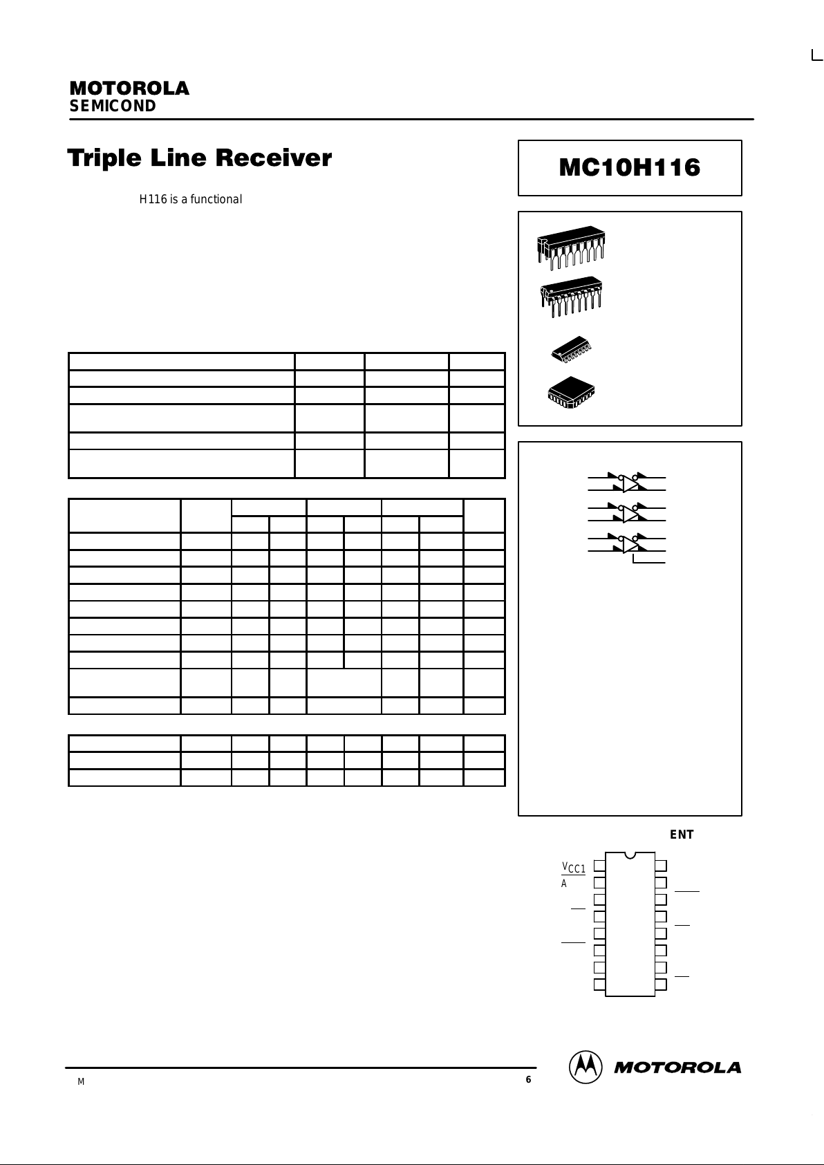
LOGIC DIAGRAM
DIP PIN ASSIGNMENT
V
CC1
A
OUT
A
OUT
A
IN
A
IN
B
OUT
B
OUT
V
EE
V
CC2
C
OUT
C
OUT
C
IN
C
IN
V
BB
B
IN
B
IN
16
15
14
13
12
11
10
9
1
2
3
4
5
6
7
8
5
4
11
3
2
10
9
7
6
13
12
15
14
*VBB to be used to supply bias to the MC10H116 only
and bypassed (when used) with 0.01 µF to 0.1 µF
capacitor to ground (0 V). VBB can source < 1.0 mA.
The MC10H116 is designed to be used in sensing
differential signals over long lines. The bias supply
(VBB) is made available to make the device useful as a
Schmitt trigger, or in other applications where a stable
reference voltage is necessary.
Active current sources provide these receivers with
excellent common–mode noise rejection. If any amplifier in a package is not used, one input of that amplifier
must be connected to VBB to prevent unbalancing the
current–source bias network.
The MC10H116 does not have internal–input pulldown resistors. This provides high impedance to the
amplifier input and facilitates differential connections.
Applications:
• Low Level Receiver • Voltage Level
• Schmitt Trigger Interface
When input pin with
bubble goes positive
it’s respective output
pin with bubble goes
positive.
V
CC1
= Pin 1
V
CC2
= Pin 16
VEE = Pin 8
VBB*
L SUFFIX
CERAMIC PACKAGE
CASE 620–10
P SUFFIX
PLASTIC PACKAGE
CASE 648–08
D SUFFIX
PLASTIC SOIC
CASE 751B–05
FN SUFFIX
PLCC
CASE 775–02
Pin assignment is for Dual–in–Line Package.
For PLCC pin assignment, see the Pin Conversion
T ables on page 6–11 of the Motorola MECL Data
Book (DL122/D).
MC10H116
MOTOROLA MECL Data
DL122 — Rev 6
2–220
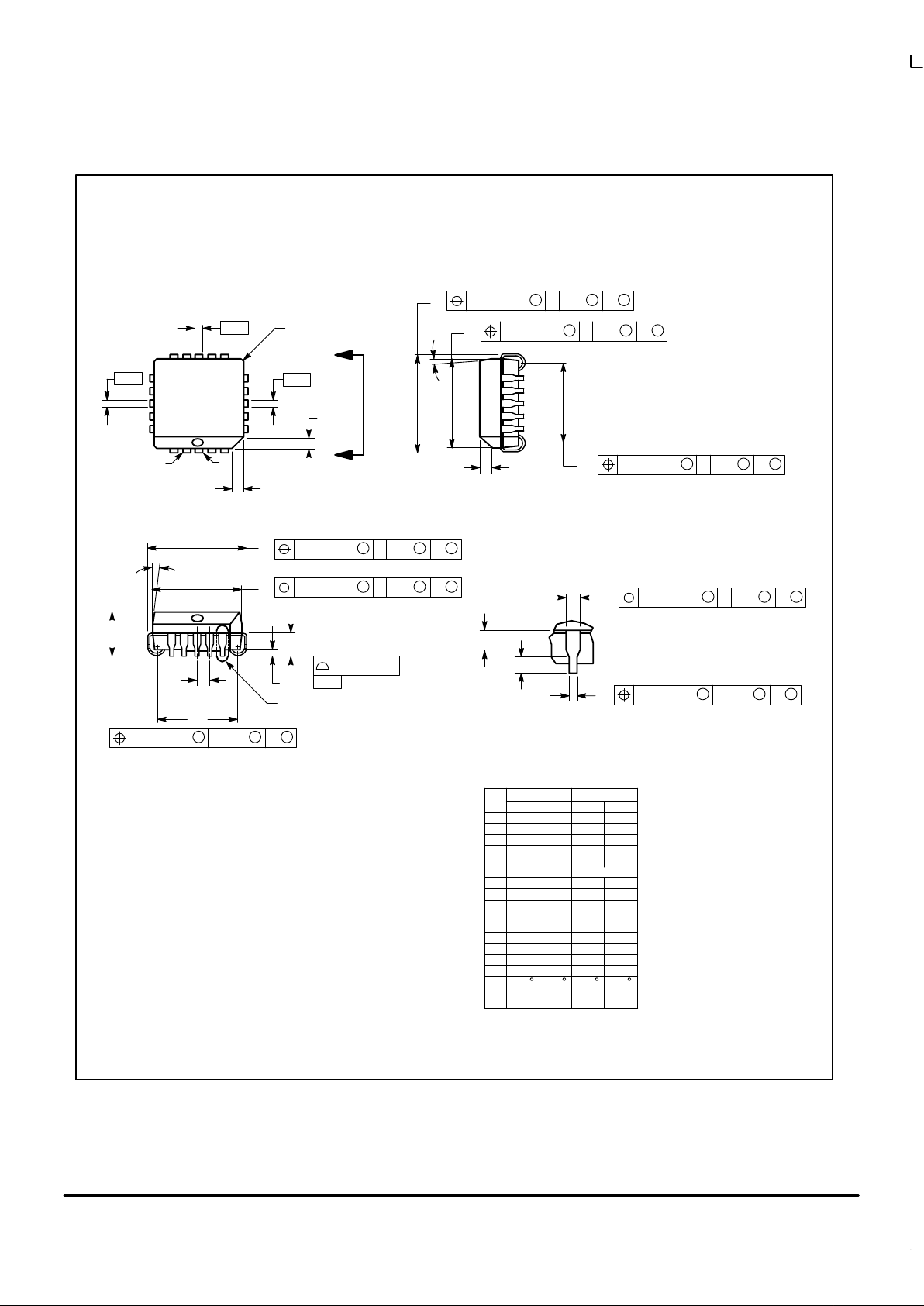
OUTLINE DIMENSIONS
FN SUFFIX
PLASTIC PLCC PACKAGE
CASE 775–02
ISSUE C
NOTES:
1. DATUMS –L–, –M–, AND –N– DETERMINED
WHERE TOP OF LEAD SHOULDER EXITS PLASTIC
BODY AT MOLD PARTING LINE.
2. DIMENSION G1, TRUE POSITION TO BE
MEASURED AT DATUM –T–, SEATING PLANE.
3. DIMENSIONS R AND U DO NOT INCLUDE MOLD
FLASH. ALLOWABLE MOLD FLASH IS 0.010 (0.250)
PER SIDE.
4. DIMENSIONING AND TOLERANCING PER ANSI
Y14.5M, 1982.
5. CONTROLLING DIMENSION: INCH.
6. THE PACKAGE TOP MAY BE SMALLER THAN THE
PACKAGE BOTTOM BY UP TO 0.012 (0.300).
DIMENSIONS R AND U ARE DETERMINED AT THE
OUTERMOST EXTREMES OF THE PLASTIC BODY
EXCLUSIVE OF MOLD FLASH, TIE BAR BURRS,
GATE BURRS AND INTERLEAD FLASH, BUT
INCLUDING ANY MISMATCH BETWEEN THE TOP
AND BOTTOM OF THE PLASTIC BODY.
7. DIMENSION H DOES NOT INCLUDE DAMBAR
PROTRUSION OR INTRUSION. THE DAMBAR
PROTRUSION(S) SHALL NOT CAUSE THE H
DIMENSION TO BE GREATER THAN 0.037 (0.940).
THE DAMBAR INTRUSION(S) SHALL NOT CAUSE
THE H DIMENSION TO BE SMALLER THAN 0.025
(0.635).
–M–
–N–
–L–
Y BRK
W
V
D
D
S
L–M
M
0.007 (0.180) N
S
T
S
L–M
M
0.007 (0.180) N
S
T
S
L–M
S
0.010 (0.250) N
S
T
X
G1
B
U
Z
VIEW D–D
20 1
S
L–M
M
0.007 (0.180) N
S
T
S
L–M
M
0.007 (0.180) N
S
T
S
L–M
S
0.010 (0.250) N
S
T
C
G
VIEW S
E
J
R
Z
A
0.004 (0.100)
–T–
SEATING
PLANE
S
L–M
M
0.007 (0.180) N
S
T
S
L–M
M
0.007 (0.180) N
S
T
H
VIEW S
K
K1
F
G1
DIM MIN MAX MIN MAX
MILLIMETERSINCHES
A 0.385 0.395 9.78 10.03
B 0.385 0.395 9.78 10.03
C 0.165 0.180 4.20 4.57
E 0.090 0.110 2.29 2.79
F 0.013 0.019 0.33 0.48
G 0.050 BSC 1.27 BSC
H 0.026 0.032 0.66 0.81
J 0.020 ––– 0.51 –––
K 0.025 ––– 0.64 –––
R 0.350 0.356 8.89 9.04
U 0.350 0.356 8.89 9.04
V 0.042 0.048 1.07 1.21
W 0.042 0.048 1.07 1.21
X 0.042 0.056 1.07 1.42
Y ––– 0.020 ––– 0.50
Z 2 10 2 10
G1 0.310 0.330 7.88 8.38
K1 0.040 ––– 1.02 –––
____
 Loading...