

Motorola MC10E457FNR2, MC10E457FN, MC100E457FN, MC100E457FNR2 Datasheet
SEL0
0
a VBBD0b D0b
COMSEL
V
CCO
SEL1
D1a
D1a
V
EE
V
BB
D1b
D1b
26
27
28
2
3
4
25 24 23 22 21 20 19
18
17
16
15
14
13
12
115 6 7 8 9 10
SEL2 D2a D
2
a VBBD2b D2b
Q
2
Q
2
V
CC
Q
1
Q
1
Q
0
Q
0
D0a
1
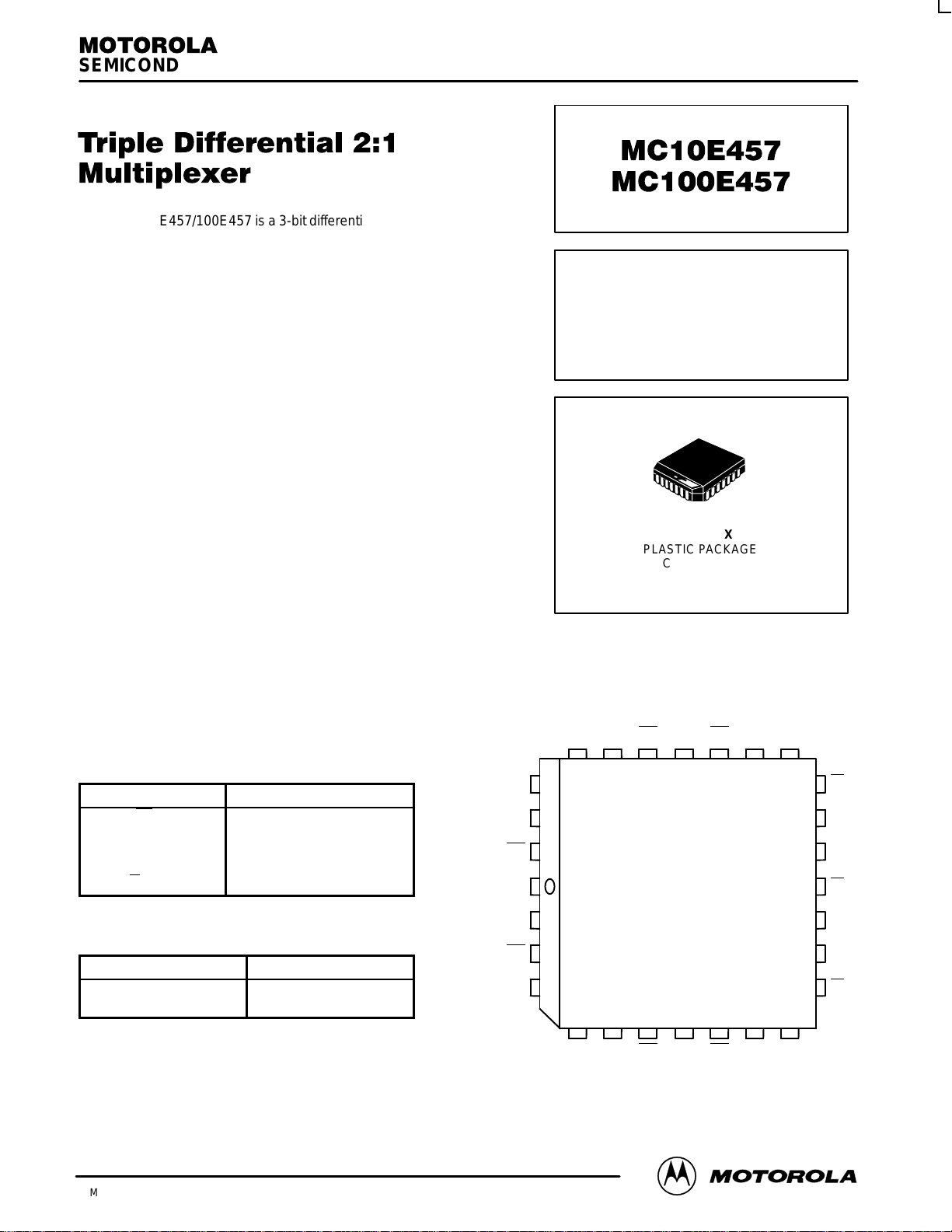
Pinout: 28-Lead PLCC (Top View)
* All VCC and V
CCO
pins are tied together on the die.
SEMICONDUCTOR TECHNICAL DATA
2–1
REV 2
Motorola, Inc. 1996
12/93
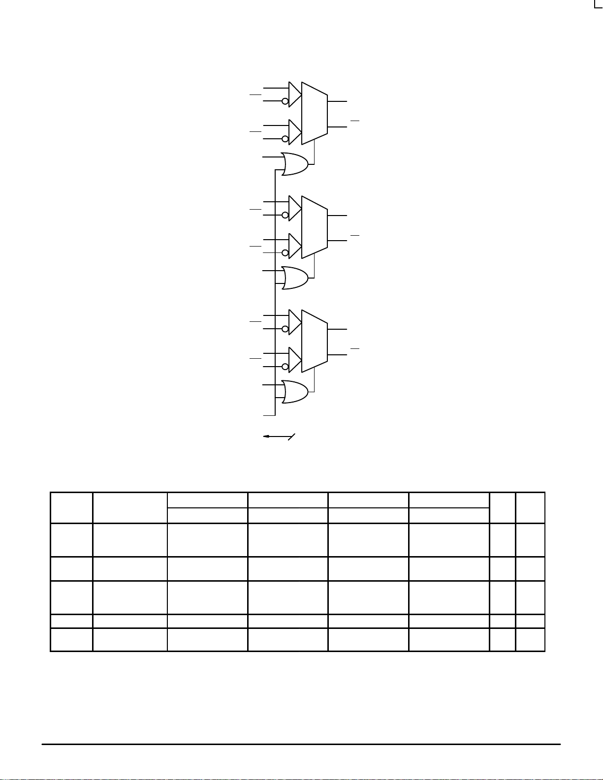
The MC10E457/100E457 is a 3-bit differential 2:1 multiplexer . The fully
differential data path makes the device ideal for multiplexing low skew
clock or other skew sensitive signals. Multiple VBB pins are provided to
ease AC coupling input signals.
The higher frequency outputs provide the device with a >1.0GHz
bandwidth to meet the needs of the most demanding system clock.
Both, separate selects and a common select, are provided to make the
device well suited for both data path and random logic applications.
The differential inputs have internal clamp structures which will force
the Q output of a gate in an open input condition to go to a LOW state.
Thus, inputs of unused gates can be left open and will not affect the
operation of the rest of the device. Note that the input clamp will take
affect only if both inputs fall 2.5V below VCC.
• Differential D and Q; V
BB
available
• 700ps Max. Propagation Delay
• High Frequency Outputs
• Separate and Common Select
• Extended 100E V
EE
Range of –4.2V to –5.46V
• Internal 75kΩ Input Pulldown Resistors
PIN NAMES
Pin Function
Dn[0:2]; Dn[0:2] Differential Data Inputs
SEL Individual Select Input
COMSEL Common Select Input
V
BB
VBB Reference Output
Q[0:2], Q[0:2] Differential Data Outputs
FUNCTION TABLE
SEL Data
H a
L b
TRIPLE DIFFERENTIAL
2:1 MULTIPLEXER
FN SUFFIX
PLASTIC PACKAGE
CASE 776-02
D
MC10E457 MC100E457
MOTOROLA ECLinPS and ECLinPS Lite
DL140 — Rev 4
2–2
LOGIC DIAGRAM
D0a
D
0
a
D0b
D
0
b
SEL0
D1a
D
1
a
D1b
D
1
b
SEL1
D2a
D2a
D2b
D
2
b
SEL2
COMSEL
V
BB
Q
0
Q
0
Q
1
Q
1
Q
2
Q
2
H
L
2:1
MUX
H
L
2:1
MUX
H
L
2:1
MUX
DC CHARACTERISTICS (VEE = VEE(min) to VEE(max); VCC = V
CCO
= GND)
–40°C 0°C 25°C 85°C
Symbol Characteristic Min Typ Max Min Typ Max Min Typ Max Min Typ Max Unit Cond
V
BB
Output Reference
Voltage 10E
100E
–1.43
–1.38
–1.30
–1.26
–1.38
–1.38
–1.27
–1.26
–1.35
–1.38
–1.25
–1.26
–1.31
–1.38
–1.19
–1.26
V
I
IH
Input HIGH
Current
150 150 150 150 µA
I
EE
Power Supply
Current 10E
100E
9292110
110
9292110
110
9292110
110
92
106
110
127
mA
VPP(DC) Input Sensitivity 50 50 50 50 mV 1
V
CMR
Commom Mode
Range
–1.5 0 –1.5 0 –1.5 0 –1.5 0 V 2
1. Differential input voltage required to obtain a full ECL swing on the outputs.
2. V
CMR
is defined as the range within which the VIH level may vary, with the device still meeting the propagation delay specification. The VIL level
must be such that the peak to peak voltage is less than 1.0 V and greater than or equal to VPP(min).
 Loading...