

Motorola MC10E451FN, MC10E451FNR2, MC100E451FN, MC100E451FNR2 Datasheet
D1D1D2D2V
CCO
D
3
D
3
D
4
D
4
D
5
D
5
V
CCO
Q
0
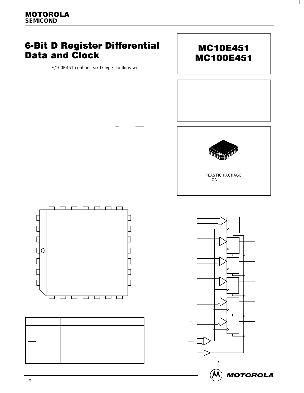
LOGIC DIAGRAM
CLK
V
BB
CLK
V
EE
MR
NC
D
0
26
27
28
2
3
4
25 24 23 22 21 20 19
18
17
16
15
14
13
12
115 6 7 8 9 10
Q
5
Q
4
V
CC
Q
3
V
CCO
Q
2
Q
1
D
0
D
0
D
0
D
1
D
1
D
2
D
2
D
3
D
3
D
4
D
4
D
5
D
5
CLK
CLK
MR
V
BB
Q
0
Q
1
Q
2
Q
3
Q
4
Q
5
D
R
D
R
D
R
D
R
D
R
D
R
1
Pinout: 28-Lead PLCC
(Top View)
* All VCC and V
CCO
pins are tied together on the die.
SEMICONDUCTOR TECHNICAL DATA
2–1
REV 2
Motorola, Inc. 1996
12/93
The MC10E/100E451 contains six D-type flip-flops with single-ended
outputs and differential data inputs. The common clock input is also
differential. The registers are triggered by a positive transition of the
positive clock (CLK) input.
A HIGH on the Master Reset (MR) input resets all Q outputs to LOW.
The VBB output is intended for use as a reference voltage for
single-ended reception of ECL signals to that device only . When using for
this purpose, it is recommended that VBB is decoupled to VCC via a
0.01µF capacitor.
The differential input structures are clamped so that the inputs of
unused registers can be left open without upsetting the bias network of
the device. The clamping action will assert the D
and the CLK sides of the
inputs. Because of the edge triggered flip-flop nature of the device
simultaneously opening both the clock and data inputs will result in an
output which reaches an unidentified but valid state. Note that the input
clamps only operate when both inputs fall to 2.5V below VCC.
• Differential Inputs: Data and Clock
• V
BB
Output
• 1100MHz Min. Toggle Frequency
• Asynchronous Master Reset
• Extended 100E V
EE
Range of – 4.2V to – 5.46V
• 75kΩ Input Pulldown Resistors
PIN NAMES
Pin Function
D0– D
5
+Data Input
D
0
– D
5
– Data Input
CLK +Clock Input
CLK – Clock Input
MR Master Reset Input
V
BB
VBB Output
Q0– Q
5
Data Outputs
6-BIT D REGISTER
DIFFERENTIAL
DATA AND CLOCK
FN SUFFIX
PLASTIC PACKAGE
CASE 776-02
MC10E451 MC100E451
MOTOROLA ECLinPS and ECLinPS Lite
DL140 — Rev 4
2–2
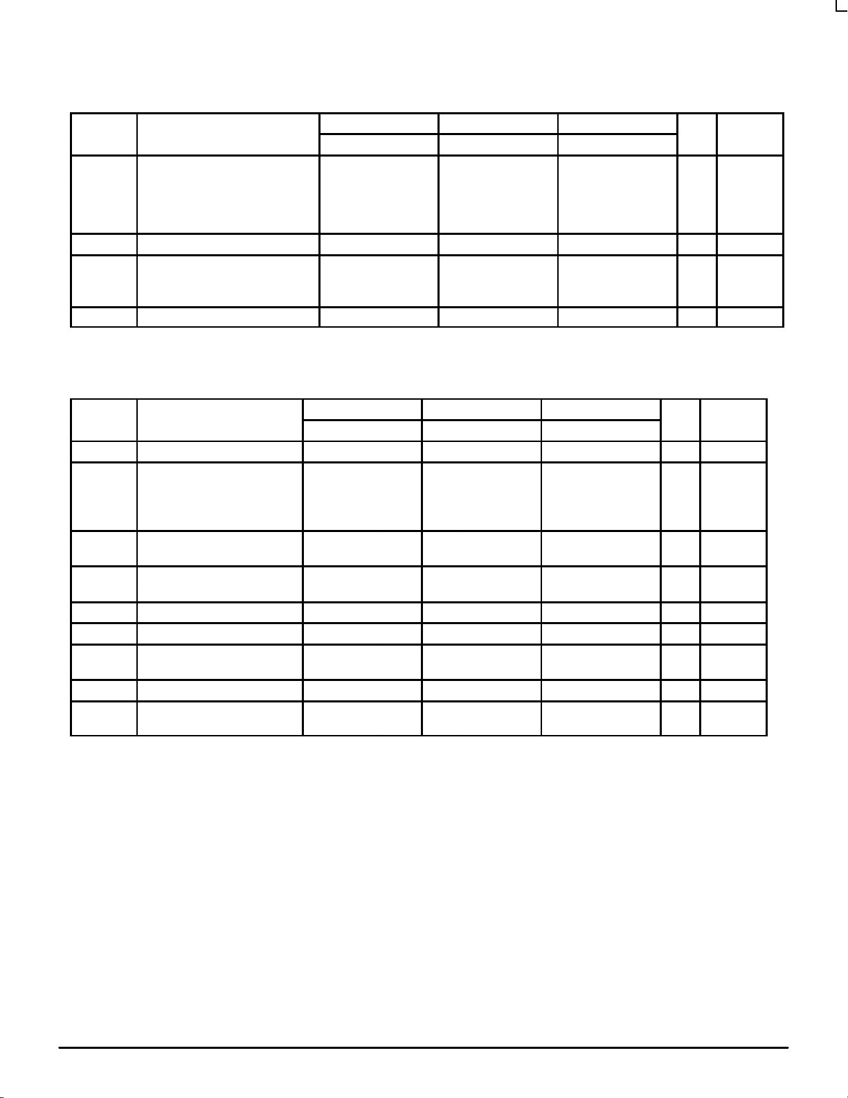
DC CHARACTERISTICS (VEE = VEE(min) to VEE(max); VCC = V
CCO
= GND)
0°C 25°C 85°C
Symbol Characteristic min typ max min typ max min typ max Unit Condition
V
BB
Output Reference Voltage V
10E –1.3
8
–1.27–1.3
5
–1.25–1.3
1
–1.1
9
100E –1.3
8
–1.26–1.3
8
–1.26–1.3
8
–1.2
6
I
IH
Input HIGH Current 150 150 150 µA
I
EE
Power Supply Current mA
10E 84 101 84 101 84 101
100E 84 101 84 101 97 116
V
CMR
Common Mode Range – 2.0 – 0.4 – 2.0 – 0.4 – 2.0 – 0.4 V 2
1. V
CMR
is referenced to the most positive side of the differential input signal. Normal operation is obtained when the “HIGH” input is within the
V
CMR
range and the input swing is greater than VPP
MIN
and < 1.0V.
AC CHARACTERISTICS (VEE = VEE(min) to VEE(max); VCC = V
CCO
= GND)
0°C 25°C 85°C
Symbol Characteristic min typ max min typ max min typ max Unit Condition
f
MAX
Max, Toggle Frequency 1100 1400 1100 1400 1100 1400 MHz
t
PLH
Propagation Delay to Output ps
t
PHL
CLK (Diff) 475 650 800 475 650 800 475 650 800
CLK (SE) 425 650 850 425 650 850 425 650 850
MR 425 600 850 425 600 850 425 600 850
t
s
Setup Time ps
D 150 –100 150 –100 150 –100
t
h
Hold Time ps
D 250 100 250 100 250 100
VPP(AC) Minimum Input Swing 150 150 159 mV 1
t
RR
Reset Recovery Time 750 600 750 600 750 600 ps
t
PW
Minimum Pulse Width ps
CLK, MR 400 400 400
t
SKEW
Within-Device Skew 100 100 100 ps 2
t
r
Rise/Fall Times ps
t
f
20 - 80% 275 450 800 275 450 800 275 450 800
1. Minimum input voltage for which AC parameters are guaranteed.
2. Within-device skew is defined as identical transitions on similar paths through a device.
 Loading...