

Motorola MC10E446FN, MC100E446FN, MC100E446FNR2, MC10E446FNR2 Datasheet
NCNCMODED1D0
V
CCO
CL/4
CL/4V
CCO
CL/8CL/8V
CCO
NC
NC
V
CC
SOUT
SOUT
V
CCO
NC
CLK
CLK
V
BB
V
EE
SIN
SIN
SYNC
18
17
16
15
14
13
12
19202122232425
111098765
26
27
28
1
2
3
4
D3D2
SEMICONDUCTOR TECHNICAL DATA
2–1
REV 2
Motorola, Inc. 1996
7/96
The MC10E/100E446 is an integrated 4-bit parallel to serial data
converter. The device is designed to operate for NRZ data rates of up to
1.3Gb/s. The chip generates a divide by 4 and a divide by 8 clock for both
4-bit conversion and a two chip 8-bit conversion function. The conversion
sequence was chosen to convert the parallel data into a serial stream
from bit D0 to D3. A serial input is provided to cascade two E446 devices
for 8 bit conversion applications. Note that the serial output data clocks off
of the negative input clock transition.
• On Chip Clock ÷4 and ÷8
• 1.5 Gb/s Typical Data Rate Capability
• Differential Clock and Serial Inputs
• V
BB
Output for Single-ended Input Applications
• Asynchronous Data Synchronization
• Mode Select to Expand to 8 Bits
• Internal 75kΩ Input Pulldown Resistors
• Extended 100E V
EE
Range of -4.2V to -5.46V
The SYNC input will asynchronously reset the internal clock circuitry.
This pin allows the user to reset the internal clock conversion unit and
thus select the start of the conversion process.
The MODE input is used to select the conversion mode of the device.
With the MODE input LOW, or open, the device will function as a 4-bit
converter. When the mode input is driven HIGH the internal load clock will
change on every eighth clock cycle thus allowing for an 8-bit conversion scheme using two E446’s. When cascaded in an 8-bit
conversion scheme the devices will not operate at the 1.3Gb/s data rate of a single device. Refer to the applications section of
this data sheet for more information on cascading the E446.
For lower data rate applications a VBB reference voltage is supplied for single-ended inputs. When operating at clock rates
above 500MHz differential input signals are recommended. For single-ended inputs the VBB pin is tied to the inverting differential
input and bypassed via a 0.01µF capacitor. The VBB provides the switching reference for the input differential amplifier . The V
BB
can also be used to AC couple an input signal, for more information on AC coupling refer to the interfacing section of the design
guide in the ECLinPS data book.
PIN NAMES
Pin Function
SIN
D0 – D3
SOUT, SOUT
CLK, CLK
CL/4, CL/4
CL/8, CL/8
MODE
SYNC
Differential Serial Data Input
Parallel Data Inputs
Differential Serial Data Output
Differential Clock Inputs
Differential ÷4 Clock Output
Differential ÷8 Clock Output
Conversion Mode 4-Bit/8-Bit
Conversion Synchronizing Input
FUNCTION TABLES
Mode Conversion
L
H
4-Bit
8-Bit
4-BIT PARALLEL/
SERIAL CONVERTER
FN SUFFIX
PLASTIC PACKAGE
CASE 776-02
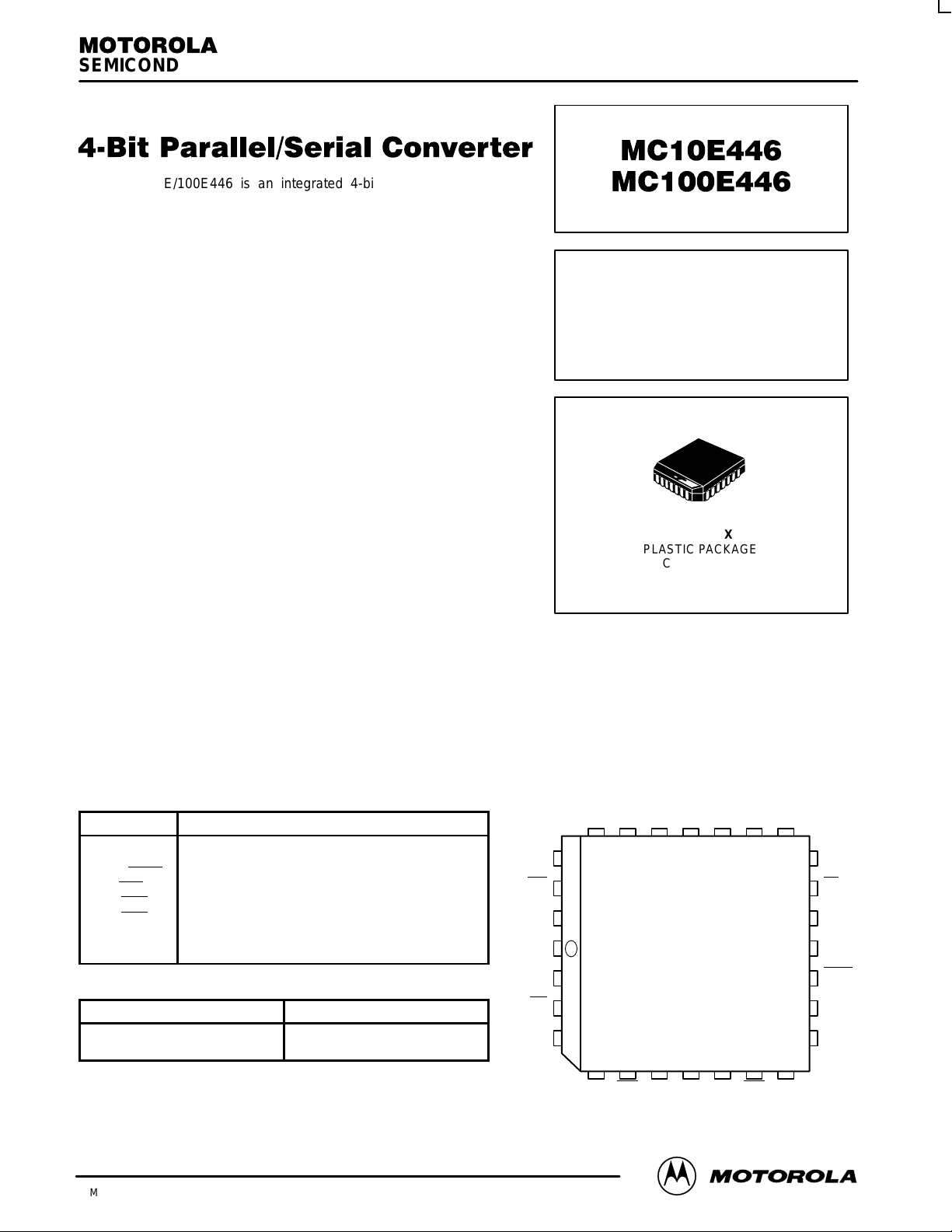
Pinout: 28-Lead PLCC (Top View)

MC10E446 MC100E446
MOTOROLA ECLinPS and ECLinPS Lite
DL140 — Rev 4
2–2
LOGIC DIAGRAM
QD
SIN
SOUT
SOUT
CL/4
CL/4
0
1
SIN
CLK
CLK
D3
CLK
QD
0
1
D2
CLK
QD
0
1
D1
CLK
QD
0
1
D0
CLK
0 1
R
÷
4
R
÷
8
CL/8
CL/8
Mode
SYNC
Delay
LOAD PULSE
GENERATOR
 Loading...