


LOGIC DIAGRAM
25 24 23 22 21 20 19
18
17
16
15
14
13
12
5 6 7 8 9 10 11
26
27
28
2
3
4
D3a D
3
a D3b D3b V
CCOQ3
Q
3
Q
2
Q
2
V
CC
Q
1
Q
1
Q
0
Q
0
D1a D1a D0b
D2b
D2b
D
2
a
V
EE
D2a
D
1
b
D1b
D0b D
0
a D0a V
CCO
D0a
D
0
a
D0b
D
0
b
D1a
D
1
a
D1b
D
1
b
D2a
D
2
a
D2b
D
2
b
D3a
D
3
a
D3b
D
3
b
Q
0
Q
0
Q
1
Q
1
Q
2
Q
2
Q
3
Q
3
1
Pinout: 28-Lead PLCC
(Top View)
* All VCC and V
CCO
pins are tied together on the die.
SEMICONDUCTOR TECHNICAL DATA
2–1
REV 2
Motorola, Inc. 1996
12/93
The MC10E404/100E404 is a 4-bit differential AND/NAND device. The
differential operation of the device makes it ideal for pulse shaping
applications where duty cycle skew is critical. Special design techniques
were incorporated to minimize the skew between the upper and lower
level gate inputs.
Because a negative 2-input NAND function is equivalent to a 2-input
OR function, the differential inputs and outputs of the device also allow for
its use as a fully differential 2 input OR/NOR function.
The output RISE/FALL times of this device are significantly faster than
most other standard ECLinPS devices resulting in an increased
bandwidth.
The differential inputs have clamp structures which will force the Q
output of a gate in an open input condition to go to a LOW state. Thus,
inputs of unused gates can be left open and will not affect the operation of
the rest of the device. Note that the input clamp will take affect only if both
inputs fall 2.5V below VCC.
• Differential D and Q
• 700ps Max. Propagation Delay
• High Frequency Outputs
• Extended 100E V
EE
Range of – 4.2V to – 5.46V
• Internal 75kΩ Input Pulldown Resistors
PIN NAMES
Pin Function
D[0:4], D[0:4] Differential Data Inputs
Q[0:4], Q[0:4] Differential Data Outputs
FUNCTION TABLE
Da Db Q Da Db Q
L L L L L L
L H L L H H
H L L H L H
H H H H H H
QUAD DIFFERENTIAL
AND/NAND
FN SUFFIX
PLASTIC PACKAGE
CASE 776-02
MC10E404 MC100E404
MOTOROLA ECLinPS and ECLinPS Lite
DL140 — Rev 4
2–2
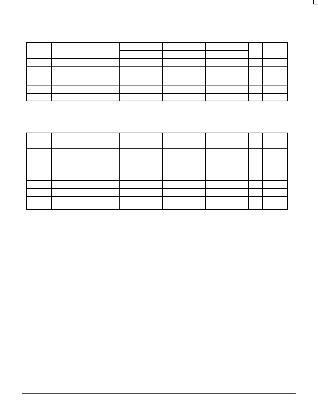
DC CHARACTERISTICS (VEE = VEE(min) to VEE(max); VCC = V
CCO
= GND)
0°C 25°C 85°C
Symbol Characteristic min typ max min typ max min typ max Unit Condition
I
IH
Input HIGH Current 150 150 150 µA
I
EE
Power Supply Current mA
10E 106 127 106 127 106 127
100E 106 127 106 127 122 146
VPP(DC) Input Sensitivity 50 50 50 mV 1
V
CMR
Common Mode Range –1.5 0 –1.5 0 –1.5 0 V 2
1. Differential input voltage required to obtain a full ECL swing on the outputs.
2. V
CMR
is referenced to the most positive side of the differential input signal. Normal operation is obtained when the input signals are within the
V
CMR
range and the input swing is greater than VPP
MIN
and < 1.0V.
AC CHARACTERISTICS (VEE= VEE(min) to VEE(max); VCC = V
CCO
= GND)
0°C 25°C 85°C
Symbol Characteristic min typ max min typ max min typ max Unit Condition
t
PLH
Propagation Delay to Output ps
t
PHL
Da (Diff) 350 475 650 350 475 650 350 475 650
Da (SE) 300 475 700 300 475 700 300 475 700
Db (Diff) 375 500 675 375 500 675 375 500 675
Db (SE) 325 500 725 325 500 725 325 500 725
t
SKEW
Within-Device Skew 50 50 50 ps 1
VPP(AC) Minimum Input Swing 150 150 150 mV 2
t
r
Rise/Fall Time
t
f
20 - 80% 150 400 150 400 150 400 ps
1. Within-device skew is defined as identical transitions on similar paths through a device.
2. Minimum input swing for which AC parameters are guaranteed.
 Loading...