

MOTOROLA MC100LVE210FN, MC100LVE210FNR2, MC100E210FNR2, MC100E210FN Datasheet
MC100LVE210, MC100E210
Low Voltage Dual 1:4, 1:5
Differential Fanout Buffer
ECL/PECL Compatible
The MC100LVE210 is a low voltage, low skew dual differential
ECL fanout buffer designed with clock distribution in mind. The
device features two fanout buffers, a 1:4 and a 1:5 buffer, on a single
chip. The device features fully differential clock paths to minimize
both device and system skew. The dual buf fer allows for the fanout of
two signals through a single chip, thus reducing the skew between the
two fundamental signals from a part–to–part skew down to an
output–to–output skew . This capability reduces the skew by a factor of
4 as compared to using two LVE111’s to accomplish the same task.
The MC100LVE210 works from a –3.3V supply while the
MC100E210 provides identical function and performance from a
standard –4.5V 100E voltage supply .
For applications which require a single–ended input, the V
BB
reference voltage is supplied. For single–ended input applications the
VBB reference should be connected to the unused CLK input of a
differential pair and bypassed to ground via a 0.01µf capacitor. The
input signal is then driven into the selected CLK input.
T o ensure that the tight skew specification is met it is necessary that
both sides of the differential output are identically terminated, even if
only one side is being used. In most applications all nine differential
pairs will be used and therefore terminated. In the case where fewer
than nine pairs are used it is necessary to terminate at least the output
pairs adjacent to the output pair being used in order to maintain
minimum skew. Failure to follow this guideline will result in small
degradations of propagation delay (on the order of 10–20ps) of the
outputs being used, while not catastrophic to most designs this will
result in an increase in skew. Note that the package corners isolate
outputs from one another such that the guideline expressed above
holds only for outputs on the same side of the package.
The MC100LVE210, as with most ECL devices, can be operated
from a positive VCC supply in PECL mode. This allows the L VE210 to
be used for high performance clock distribution in +3.3V systems.
Designers can take advantage of the LVE210’s performance to
distribute low skew clocks across the backplane or the board. In a
PECL environment series or Thevenin line terminations are typically
used as they require no additional power supplies, if parallel
termination is desired a terminating voltage of VCC–2.0V will need to
be provided. For more information on using PECL, designers should
refer to Application Note AN1406/D.
• Dual Differential Fanout Buf fers
• 200ps Part–to–Part Skew
• 50ps Typical Output–to–Output Skew
• Low Voltage ECL/PECL Compatible
• 28–lead PLCC Packaging
http://onsemi.com
PLCC PACKAGE
FN SUFFIX
CASE 776
MARKING DIAGRAM*
MC100L VE210
AWLYYWW
MC100E210FN
AWLYYWW
*For additional information, see Application Note
AND8002/D
ORDERING INFORMATION
Device Package Shipping
MC100L VE210FN PLCC 37 Units / Rail
MC100L VE210FNR2 PLCC 500 Tape & Reel
MC100E210FN PLCC 37 Units / Rail
MC100E210FNR2 PLCC 500 Tape & Reel
A = Assembly Location
WL = Wafer Lot
YY = Year
WW = Work Week
A = Assembly Location
WL = Wafer Lot
YY = Year
WW = Work Week
Semiconductor Components Industries, LLC, 1999
February , 2000 – Rev. 2
1 Publication Order Number:
MC100L VE210/D

MC100LVE210, MC100E210
V
EE
V
BB
CLKa
V
CC
CLKa
CLKb
CLKb
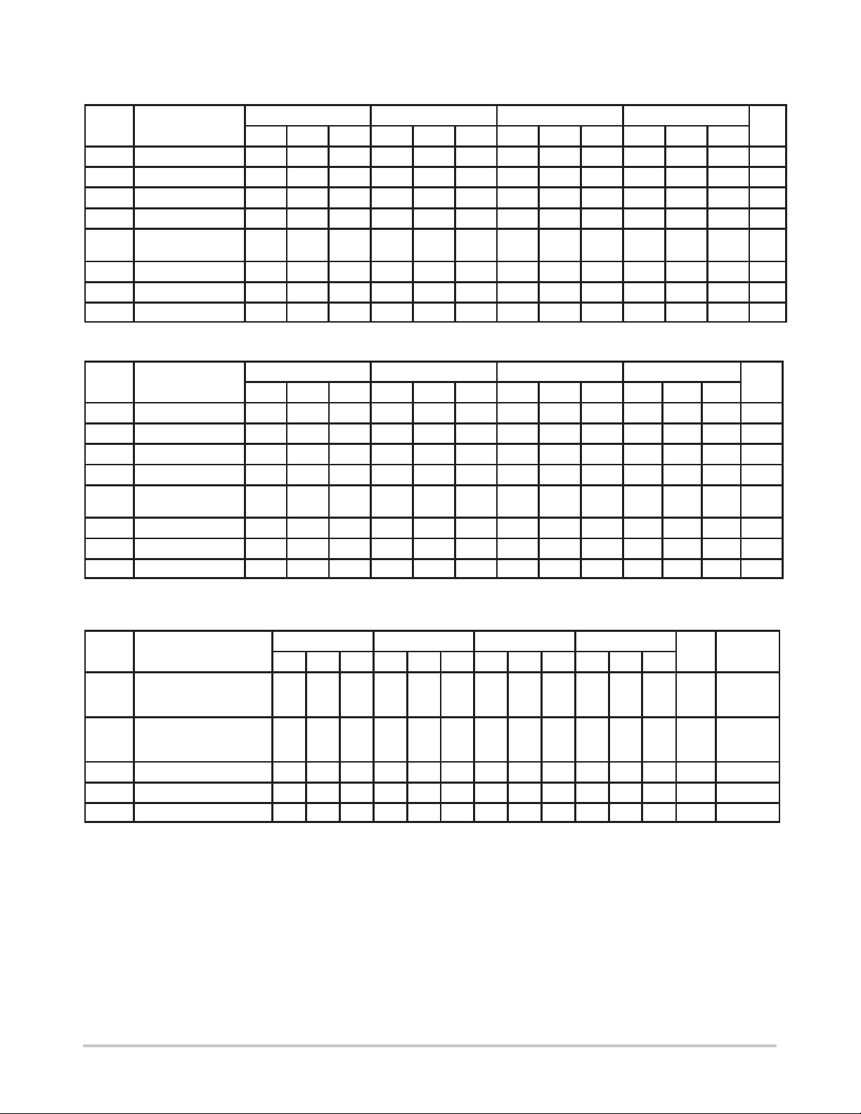
Qa0 Qa0 Qa1 V
25 24 23 22 21 20 19
26
27
28
1
2
3
4
Pinout: 28–Lead PLCC
(Top View)
567891011
Qb4 Qb3 Qb2Qb4 V
Qa1 Qa2 Qa2
CCO
Qb3 Qb2
CCO
CLKa
CLKa
Qa3
18
Qa3
17
Qb0
16
15
V
CCO
14
Qb0
13
Qb1
12
Qb1
LOGIC SYMBOL
PIN NAMES
Pins
CLKa, CLKb
Qa0:3, Qb0:4
V
BB
Qa0
Qa0
Qa1
Qa1
Qa2
Qa2
Qa3
Qa3
Function
Differential Input Pairs
Differential Outputs
VBB Output
CLKb
CLKb
V
BB
Qb0
Qb0
Qb1
Qb1
Qb2
Qb2
Qb3
Qb3
Qb4
Qb4
http://onsemi.com
2
MC100LVE210, MC100E210
MC100LVE210
ECL DC CHARACTERISTICS
–40°C 0°C 25°C 85°C
Symbol Characteristic Min Typ Max Min Typ Max Min Typ Max Min Typ Max Unit
V
OH
V
OL
V
IH
V
IL
V
BB
V
EE
I
IH
I
EE
MC100L VE210
PECL DC CHARACTERISTICS
Symbol Characteristic Min Typ Max Min Typ Max Min Typ Max Min Typ Max Unit
V
OH
V
OL
V
IH
V
IL
V
BB
V
CC
I
IH
I
EE
1. These values are for VCC = 3.3V. Level Specifications will vary 1:1 with VCC.
MC100LVE210
AC CHARACTERISTICS (VEE = VEE (min) to VEE (max); VCC = V
Symbol Characteristic Min Typ Max Min Typ Max Min Typ Max Min Typ Max Unit Condition
t
PLH
t
PHL
t
skew
V
PP
V
CMR
tr/t
1. The differential propagation delay is defined as the delay from the crossing points of the dif ferential input signals to the crossing point of the
2. The single-ended propagation delay is defined as the delay from the 50% point of the input signal to the 50% point of the output signal.
3. The within–device skew is defined as the worst case difference between any two similar delay paths within a single device.
4. VPP(min) is defined as the minimum input differential voltage which will cause no increase in the propagation delay . The VPP(min) is AC limited
5. V
Output HIGH Voltage –1.085 –1.005 –0.880 –1.025 –0.955 –0.880 –1.025 –0.955 –0.880 –1.025 –0.955 –0.880 V
Output LOW Voltage –1.830 –1.695 –1.555 –1.810 –1.705 –1.620 –1.810 –1.705 –1.620 –1.810 –1.705 –1.620 V
Input HIGH Voltage –1.165 –0.880 –1.165 –0.880 –1.165 –0.880 –1.165 –0.880 V
Input LOW Voltage –1.810 –1.475 –1.810 –1.475 –1.810 –1.475 –1.810 –1.475 V
Output Reference
Voltage
Power Supply Voltage –3.0 –3.8 –3.0 –3.8 –3.0 –3.8 –3.0 –3.8 V
Input HIGH Current 150 150 150 150 µA
Power Supply Current 55 55 55 65 mA
Output HIGH Voltage12.215 2.295 2.42 2.275 2.345 2.420 2.275 2.345 2.420 2.275 2.345 2.420 V
Output LOW Voltage11.47 1.605 1.745 1.490 1.595 1.680 1.490 1.595 1.680 1.490 1.595 1.680 V
Input HIGH Voltage
Input LOW Voltage
Output Reference
1
Voltage
Power Supply Voltage 3.0 3.8 3.0 3.8 3.0 3.8 3.0 3.8 V
Input HIGH Current 150 150 150 150 µA
Power Supply Current 55 55 55 65 mA
Propagation Delay to Output
IN (differential)
IN (single–ended)
Within–Device SkewQa Qb
Part–to–Part Skew (Diff)
Minimum Input Swing 500 500 500 500 mV Note 4
Common Mode Range –1.5 –0.4 –1.5 –0.4 –1.5 –0.4 –1.5 –0.4 V Note 5
Output Rise/Fall Time 200 600 200 600 200 600 200 600 ps 20%–80%
f
Qa Qa,Qb Qb
–1.38 –1.26 –1.38 –1.26 –1.38 –1.26 –1.38 –1.26 V
–40°C 0°C 25°C 85°C
1
2.135 2.420 2.135 2.420 2.135 2.420 2.135 2.420 V
1
1.490 1.825 1.490 1.825 1.490 1.825 1.490 1.825 V
1.92 2.04 1.92 2.04 1.92 2.04 1.92 2.04 V
= GND)
CCO
–40°C 0°C 25°C 85°C
475
400
675
700
505075
200
475
400
75
675
700
503075
200
500
450
50
700
750
503075
200
500
450
503075
50
ps
700
750
ps Note 3
50
200
differential output signals.
for the LVE210 as a differential input as low as 50 mV will still produce full ECL levels at the output.
is defined as the range within which the VIH level may vary, with the device still meeting the propagation delay specification. The V
CMR
level must be such that the peak to peak voltage is less than 1.0 V and greater than or equal to VPP(min).
Note 1
Note 2
IL
http://onsemi.com
3
 Loading...