

NC V
CCO
Q
3
V
CCO
D3bD3aNCSEL3
LOGIC DIAGRAM
D2b
D2a
SEL2
V
EE
SEL1
D1a
D1b
26
27
28
2
3
4
25 24 23 22 21 20 19
18
17
16
15
14
13
12
115 6 7 8 9 10
Q
3
Q
2
Q
2
V
CC
Q
1
Q
1
Q
0
Q
0
SEL0 D0a D0b NC NC
D0a
D0b
SEL0
D1a
D1b
SEL1
D2a
D2b
SEL2
D3a
D3b
SEL3
Q
0
Q
0
Q
1
Q
1
Q
2
Q
2
Q
3
Q
3
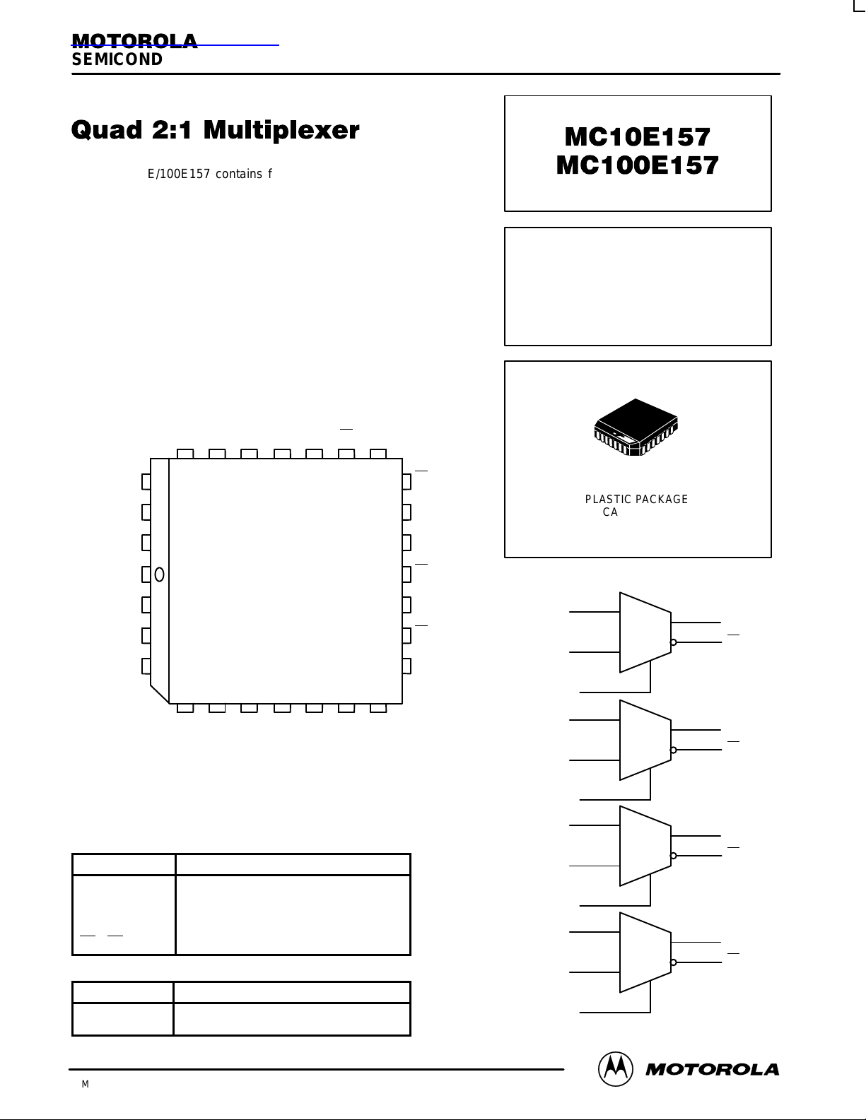
MUX
MUX
MUX
MUX
1
0
1
0
1
0
1
0
1
Pinout: 28-Lead PLCC (Top View)
* All VCC and V
CCO
pins are tied together on the die.
SEMICONDUCTOR TECHNICAL DATA
2–1
REV 2
Motorola, Inc. 1996
12/93
The MC10E/100E157 contains four 2:1 multiplexers with differential
outputs. The output data are controlled by the individual Select (SEL)
inputs. The individual select control makes the devices well suited for
random logic designs.
• Individual Select Controls
• 550ps Max. D to Output
• 800ps Max. SEL to Output
• Extended 100E V
EE
Range of – 4.2V to – 5.46V
• Internal 75kΩ Input Pulldown Resistors
PIN NAMES
Pin Function
D0a – D3a Input Data a
D0b – D3b Input Data b
SEL0 – SEL3 Select Inputs
Q0– Q
3
True Outputs
Q0– Q
3
Inverted Outputs
TRUTH TABLE
SEL Data
H
L
a
b
QUAD 2:1
MULTIPLEXER
FN SUFFIX
PLASTIC PACKAGE
CASE 776-02
查询MC100E157FNR2供应商
MC10E157 MC100E157
MOTOROLA ECLinPS and ECLinPS Lite
DL140 — Rev 4
2–2
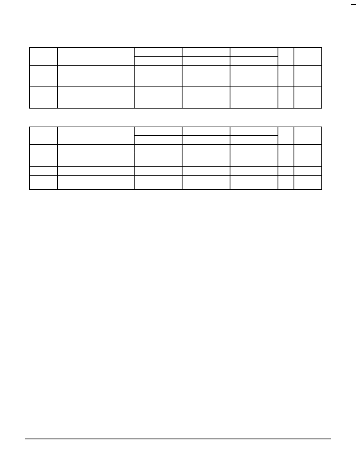
DC CHARACTERISTICS (VEE = VEE(min) to VEE(max); VCC = V
CCO
= GND)
0°C 25°C 85°C
Symbol Characteristic min typ max min typ max min typ max Unit Condition
I
IH
Input HIGH Current µA
D 200 200 200
SEL 150 150 150
I
EE
Power Supply Current mA
10E 32 38 32 38 32 38
100E 32 38 32 38 37 44
AC CHARACTERISTICS (VEE = VEE(min) to VEE(max); VCC = V
CCO
= GND)
0°C 25°C 85°C
Symbol Characteristic min typ max min typ max min typ max Unit Condition
t
PLH
Propagation Delay to Output ps
t
PHL
D 220 380 550 220 380 550 220 380 550
SEL 425 600 800 425 600 800 425 600 800
t
SKEW
Within-Device Skew 70 70 70 ps 1
t
r
Rise/Fall Times ps
t
f
20 - 80% 275 400 650 275 400 650 275 400 650
1. Within-device skew is defined as identical transitions on similar paths through a device.

MC10E157 MC100E157
2–3 MOTOROLAECLinPS and ECLinPS Lite
DL140 — Rev 4
OUTLINE DIMENSIONS
FN SUFFIX
PLASTIC PLCC PACKAGE
CASE 776–02
ISSUE D
0.007 (0.180) T L
–M
SNSM
0.007 (0.180) T L
–M
SNSM
0.007 (0.180) T L
–M
SNSM
0.010 (0.250) T L
–M
SNSS
0.007 (0.180) T L
–M
SNSM
0.010 (0.250) T L
–M
SNSS
0.007 (0.180) T L
–M
SNSM
0.007 (0.180) T L
–M
SNSM
0.004 (0.100)
SEATING
PLANE
-T-
12.32
12.32
4.20
2.29
0.33
0.66
0.51
0.64
11.43
11.43
1.07
1.07
1.07
—
2
°
10.42
1.02
12.57
12.57
4.57
2.79
0.48
0.81
—
—
11.58
11.58
1.21
1.21
1.42
0.50
10
°
10.92
—
1.27 BSC
A
B
C
E
F
G
H
J
K
R
U
V
W
X
Y
Z
G1
K1
MIN MINMAX MAX
INCHES MILLIMETERS
DIM
NOTES:
1. DATUMS -L-, -M-, AND -N- DETERMINED
WHERE TOP OF LEAD SHOULDER EXITS
PLASTIC BODY AT MOLD PARTING LINE.
2. DIM G1, TRUE POSITION TO BE MEASURED
AT DATUM -T-, SEATING PLANE.
3. DIM R AND U DO NOT INCLUDE MOLD FLASH.
ALLOWABLE MOLD FLASH IS 0.010 (0.250)
PER SIDE.
4. DIMENSIONING AND TOLERANCING PER ANSI
Y14.5M, 1982.
5. CONTROLLING DIMENSION: INCH.
6. THE PACKAGE TOP MAY BE SMALLER THAN
THE PACKAGE BOTTOM BY UP TO 0.012
(0.300). DIMENSIONS R AND U ARE
DETERMINED AT THE OUTERMOST
EXTREMES OF THE PLASTIC BODY
EXCLUSIVE OF MOLD FLASH, TIE BAR
BURRS, GATE BURRS AND INTERLEAD
FLASH, BUT INCLUDING ANY MISMATCH
BETWEEN THE TOP AND BOTTOM OF THE
PLASTIC BODY.
7. DIMENSION H DOES NOT INCLUDE DAMBAR
PROTRUSION OR INTRUSION. THE DAMBAR
PROTRUSION(S) SHALL NOT CAUSE THE H
DIMENSION TO BE GREATER THAN 0.037
(0.940). THE DAMBAR INTRUSION(S) SHALL
NOT CAUSE THE H DIMENSION TO BE
SMALLER THAN 0.025 (0.635).
VIEW S
B
U
Z
G1
X
VIEW D-D
H
K
F
VIEW S
G
C
Z
A
R
E
J
0.485
0.485
0.165
0.090
0.013
0.026
0.020
0.025
0.450
0.450
0.042
0.042
0.042
—
2
°
0.410
0.040
0.495
0.495
0.180
0.110
0.019
0.032
—
—
0.456
0.456
0.048
0.048
0.056
0.020
10
°
0.430
—
0.050 BSC
-N-
Y BRK
D
D
W
-M-
-L-
28 1
V
G1
K1

MC10E157 MC100E157
MOTOROLA ECLinPS and ECLinPS Lite
DL140 — Rev 4
2–4
Motorola reserves the right to make changes without further notice to any products herein. Motorola makes no warranty , representation or guarantee regarding
the suitability of its products for any particular purpose, nor does Motorola assume any liability arising out of the application or use of any product or circuit, and
specifically disclaims any and all liability , including without limitation consequential or incidental damages. “Typical” parameters which may be provided in Motorola
data sheets and/or specifications can and do vary in different applications and actual performance may vary over time. All operating parameters, including “Typicals”
must be validated for each customer application by customer’s technical experts. Motorola does not convey any license under its patent rights nor the rights of
others. Motorola products are not designed, intended, or authorized for use as components in systems intended for surgical implant into the body, or other
applications intended to support or sustain life, or for any other application in which the failure of the Motorola product could create a situation where personal injury
or death may occur. Should Buyer purchase or use Motorola products for any such unintended or unauthorized application, Buyer shall indemnify and hold Motorola
and its officers, employees, subsidiaries, affiliates, and distributors harmless against all claims, costs, damages, and expenses, and reasonable attorney fees
arising out of, directly or indirectly, any claim of personal injury or death associated with such unintended or unauthorized use, even if such claim alleges that
Motorola was negligent regarding the design or manufacture of the part. Motorola and are registered trademarks of Motorola, Inc. Motorola, Inc. is an Equal
Opportunity/Affirmative Action Employer.
How to reach us:
USA/EUROPE/Locations Not Listed: Motorola Literature Distribution; JAPAN: Nippon Motorola Ltd.; Tatsumi–SPD–JLDC, 6F Seibu–Butsuryu–Center,
P.O. Box 20912; Phoenix, Arizona 85036. 1–800–441–2447 or 602–303–5454 3–14–2 Tatsumi Koto–Ku, Tokyo 135, Japan. 03–81–3521–8315
MFAX: RMFAX0@email.sps.mot.com – TOUCHTONE 602–244–6609 ASIA/PACIFIC: Motorola Semiconductors H.K. Ltd.; 8B Tai Ping Industrial Park,
INTERNET: http://Design–NET.com 51 Ting Kok Road, Tai Po, N.T., Hong Kong. 852–26629298
MC10E157/D
*MC10E157/D*
◊
 Loading...