

Motorola MBRB1545CT Datasheet
SEMICONDUCTOR TECHNICAL DATA
Order this document
by MBRB1545CT/D
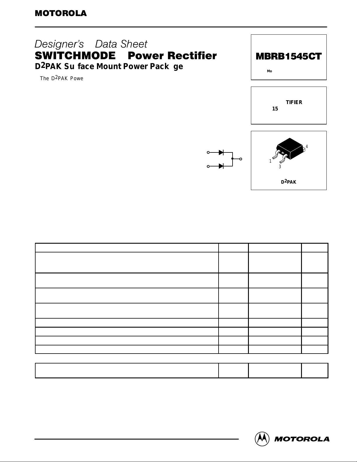
D2PAK Surface Mount Power Package
The D2PAK Power Rectifier employs the Schottky Barrier principle with a
platinum barrier metal. These state-of-the-art devices have the following
features:
• Center-Tap Configuration
• Guardring for Stress Protection
• Low Forward Voltage
• 150°C Operating Junction Temperature
• Epoxy Meets UL94, VO at 1/8″
• Guaranteed Reverse Avalanche
• Short Heat Sink Tab Manufactured — Not Sheared!
• Similar in Size to the Industry Standard TO-220 Package
Mechanical Characteristics
• Case: Epoxy, Molded
• Weight: 1.7 grams (approximately)
• Finish: All External Surfaces Corrosion Resistant and Terminal Leads are
Readily Solderable
• Lead and Mounting Surface Temperature for Soldering Purposes: 260°C
Max. for 10 Seconds
• Shipped 50 units per plastic tube
• Available in 24 mm Tape and Reel, 800 units per 13″ reel by adding a “T4”
suffix to the part number
• Marking: B1545T
1
3
Motorola Preferred Device
SCHOTTKY BARRIER
RECTIFIER
15 AMPERES
45 VOLTS
4
1
3
CASE 418B-02
D2PAK
4
MAXIMUM RATINGS, PER LEG
Rating Symbol Value Unit
Peak Repetitive Reverse Voltage
Working Peak Reverse Voltage
DC Blocking Voltage
Average Rectified Forward Current
(Rated VR) TC = 105°C Total Device
Peak Repetitive Forward Current
(Rated VR, Square Wave, 20 kHz), TC = 105°C
Non-repetitive Peak Surge Current
(Surge applied at rated load conditions halfwave, single phase, 60 Hz)
Peak Repetitive Reverse Surge Current (2.0 µs, 1.0 kHz) I
Storage Temperature T
Operating Junction Temperature T
Voltage Rate of Change (Rated VR) dv/dt 10000 V/µs
V
RRM
V
RWM
V
I
F(AV)
I
FRM
I
FSM
RRM
stg
45 Volts
R
7.5
15
15 Amps
150 Amps
1.0 Amp
–65 to +175 °C
J
–65 to +150 °C
Amps
THERMAL CHARACTERISTICS, PER LEG
Thermal Resistance — Junction to Case
— Junction to Ambient (1)
(1) When mounted using minimum recommended pad size on FR-4 board.
Designer’s Data for “Worst Case” Conditions — The Designer’s Data Sheet permits the design of most circuits entirely from the information presented. SOA Limit
curves —representing boundaries on device characteristics — are given to facilitate “worst case” design.
Designer’s and SWITCHMODE are trademarks of Motorola, Inc.
Thermal Clad is a trademark of the Bergquist Company
Preferred devices are Motorola recommended choices for future use and best overall value.
R
R
θJC
θJA
2.0
50
°C/W
Rev 2
Rectifier Device Data
Motorola, Inc. 1996
1
MBRB1545CT
ELECTRICAL CHARACTERISTICS, PER LEG
Rating Symbol Value Unit
Maximum Instantaneous Forward Voltage (2)
(iF = 7.5 Amps, TJ = 125°C)
(iF = 15 Amps, TJ = 125°C)
(iF = 15 Amps, TJ = 25°C)
Maximum Instantaneous Reverse Current (2)
(Rated dc Voltage, TJ = 125°C)
(Rated dc Voltage, TJ = 25°C)
(2) Pulse Test: Pulse Width = 300 µs, Duty Cycle ≤2.0%.
50
30
20
10
3
2
1
0.5
, INSTANTANEOUS FORWARD CURRENT (AMPS)
F
i
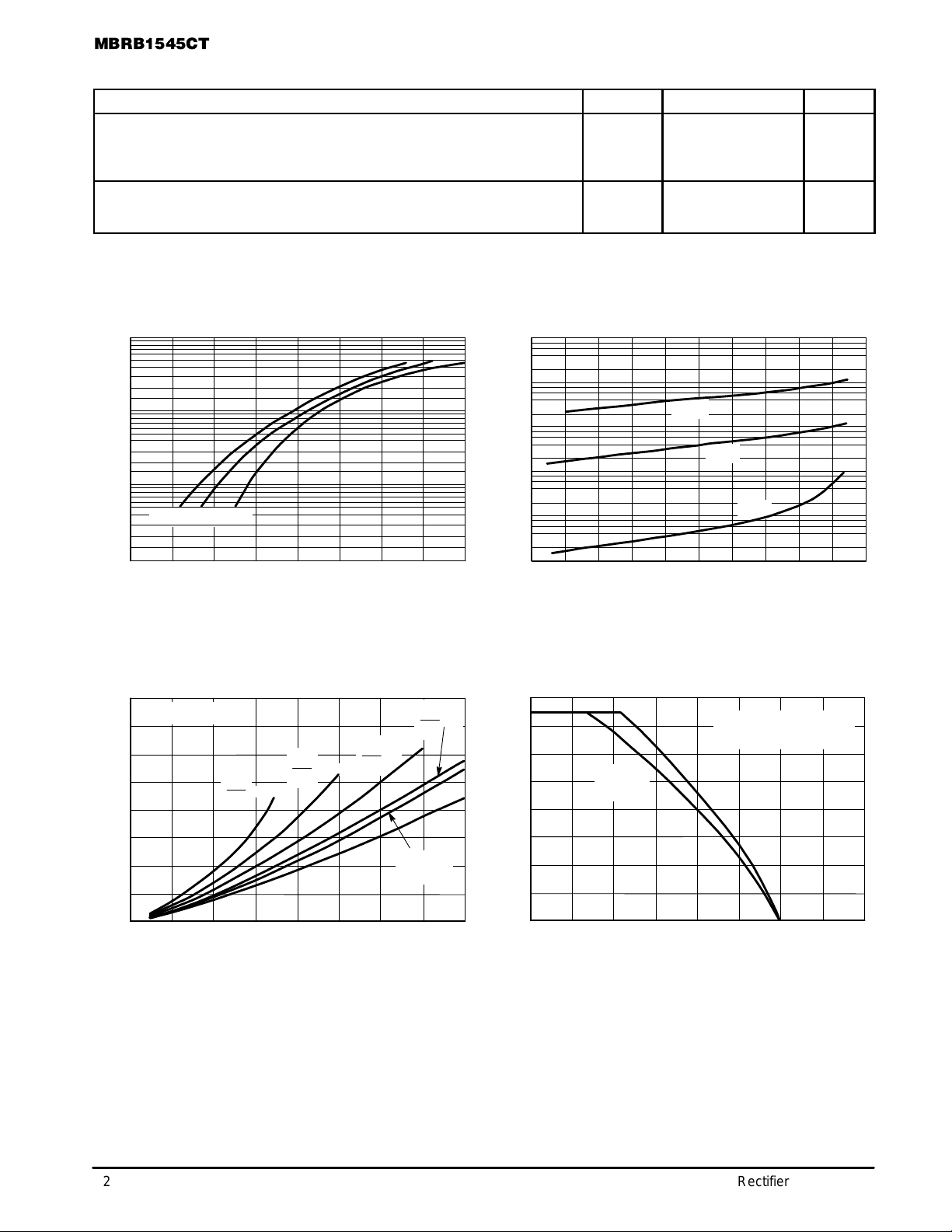
Figure 1. T ypical Forward Voltage, Per Leg
25°C85°C125°C
0.50.40.30.20.1
0.6 0.7 0.8 0.9
vF, INSTANTANEOUS FORWARD VOLTAGE (VOLTS)
0.1
0.01
, REVERSE LEAKAGE CURRENT (mA)
R
I
0.001
v
10
F
i
R
1
0
10
20
VR, REVERSE VOLTAGE (VOLTS)
0.57
0.72
0.84
15
0.1
125°C
85°C
Figure 2. T ypical Reverse Current, Per Leg
Volts
mA
25°C
504030
16
14
12
10
, AVERAGE FORWARD POWER DISSIPATION (WATTS)
F(AV)
P
= 5
SQUARE
I
PK
I
AV
WAVE
DC
=
π
1614121086420
TJ = 125°C
I
I
PK
= 10
I
= 20
AV
I
PK
I
8
6
4
2
0
I
AV
, AVERAGE FORW ARD CURRENT (AMPS)
F(AV)
I
PK
AV
16
14
12
10
8
6
4
, AVERAGE FORW ARD CURRENT (AMPS)
2
F(AV)
I
DC
SQUARE
WAVE
TC, CASE TEMPERATURE (
Figure 3. T ypical Forward Power Dissipation Figure 4. Current Derating, Case
RATED VOLTAGE APPLIED
R
°
C/W
= 2
θ
JC
150145140135130125120
155 160
°
C)
2
Rectifier Device Data
 Loading...