


Order this document by LT1585A/D
The L T1585A is a low dropout 3–terminal voltage regulator with 5A output
current capability .
Design has been optimized for low voltage applications where transient
response and minimum input voltage are critical. This voltage regulator
features a low dropout voltage and fast transient response. These
improvements make them ideal for low voltage microprocessor applications
requiring a regulated 2.5V to 3.6V output with an input supply below 7V.
Current limits is trimmed to ensure specified output current and controlled
short–circuit current. On–chip thermal limiting provides protection against
any combination of overload that would create excessive junction
temperatures. The LT1585A is available in the industry standard 3–pin
TO–220 and D2P AK power package.
Features
• Fast Transient Response
• Guaranteed Dropout Voltage at Multiple Currents
• Load Regulation: 0.05% Typ
• Trimmed Current Limit
• On–Chip Thermal Limiting
• Standard 3–Pin Power Package
Applications
• Pentium
• Power PC Supplies
• Other 2.5V to 3.6V Microprocessor Supplies
• Low Voltage Logic Supplies
• Battery–Powered Circuitry
• Post Regulator for Switching Supply
Processor Supplies
5A LOW DROPOUT FAST
RESPONSE POSITIVE
ADJUSTABLE AND FIXED
VOLTAGE REGULATOR
SILICON MONOLITHIC
INTEGRATED CIRCUIT
1
2
3
T SUFFIX
PLASTIC PACKAGE
CASE 221A
Adjustable output:
Pin 1. Adjust
Pin 2. V
out
Pin 3. V
in
Fixed 1.5V output:
Pin 1. Gnd
Pin 2. V
out
Pin 3. V
in
V
in
MOTOROLA ANALOG IC DEVICE DATA
Simplified Block Diagram
Thermal
Limit
Adjust
1
2
3
CM SUFFIX
+
–
Device
LT1585ACT 0 to 125°C TO–220
V
out
LT1585ACM 0 to 125°C D2PAK
LT1585ACT–1.5 0 to 125°C TO–220
LT1585ACM–1.5 0 to 125°C D2PAK
Motorola, Inc. 1999 Rev 0
PLASTIC PACKAGE
CASE 936
(D2PAK)
ORDERING INFORMATION
Tested
Operating
Temp.
Range
Output
Voltage
Type
ADJ.
ADJ.
FIXED
1.5V
FIXED
1.5V
Package
1
LT1585A
Á
Á
Á
ABSOLUTE MAXIMUM RATINGS
Maximum Supply Voltage
Power Dissipation
Case 221A (TO–220) (TJ = +25°C) P
Thermal Resistance, Junction–to–Ambient R
Thermal Resistance, Junction–to–Case R
Case 936 (D2PAK) (TJ = +25°C) P
Thermal Resistance, Junction–to–Ambient R
Thermal Resistance, Junction–to–Case R
Storage Temperature Range
Minimum ESD Rating (Human Body Model: C = 100pF, R = 1.5 kW)
Lead Temperature (Soldering, 10 sec.)
Maximum Junction Temperature
OPERATING RATINGS (Operating Ratings indicate conditions for which the device is intended to be functional, but do not guarantee
specific performance limits. For guaranteed specifications and test conditions, see the Electrical Characteristics)
Operating Junction Temperature Range
Supply Voltage
БББББББББББББББББ
ELECTRICAL CHARACTERISTICS (0 < T
Characteristic
Reference Voltage (LT1585A)
(Vin–V
1.5V ≤ (Vin–V
Output Voltage (LT1585A–1.5)
Vin = 5V, TJ = 25°C, I
3V ≤ Vin ≤ 7V, 0mA ≤ I
Line Regulation [Notes 1, 2]
LT1585A: 2.75V ≤ Vin ≤ 7V, I
LT1585A–1.5: 3V ≤ Vin ≤ 7V, I
Load Regulation [Notes 1, 2]
LT1585A: (Vin–V
LT1585A–1.5: Vin = 5V, TJ = 25°C, 0mA ≤ I
LT1585A: (Vin–V
LT1585A–1.5: Vin = 5V, 0mA ≤ I
Dropout Voltage
LT1585A: DV
LT1585A–1.5: DV
LT1585A: DV
LT1585A–1.5: DV
Current Limit [Note 3]
Adjust Pin Current (LT1585A)
Adjust Pin Current Change (LT1585A) [Note 3]
1.5V ≤ (Vin–V
Minimum Load Current (LT1585A) 1.5V ≤ (Vin–V
Quiescent Current (LT1585A–1.5) Vin = 5V
Ripple Rejection
LT1585A: f = 120Hz, C
LT1585A–1.5: f = 120Hz, C
Thermal Regulation TJ = 25°C, 30ms Pulse
T emperature Stability
Long Term Stability TJ = 125°C, 1000 Hrs
RMS Output Noise (% of V
NOTES 1. See thermal regulation specifications for changes in output voltage due to heating effects. Load and line regulation are measured at a constant
junction temperature by low duty cycle pulse testing.
determined by input/output differential and the output current. Guaranteed maximum output power will not be available over the full input/output voltage range.
out
(Vin–V
) = 3V, I
) = 5.5V 5.0 6.0 –
out
= 10mA, TJ = 25°C 1.238 1.250 1.262
out
) ≤ 5.75V , 10mA ≤ I
out
= 0mA 1.485 1.5 1.515
out
≤ 5A 1.470 1.5 1.530
out
) = 3V, TJ = 25°C, 10mA ≤ I
out
) = 3V, 10mA ≤ I
out
= 1%, I
REF
REF
) ≤ 5.75V , 10mA ≤ I
out
= 1%, I
OUT
= 1%, I
= 1%, I
OUT
out
OUT
OUT
= 25µF T
out
out
2.Line and load regulations are guaranteed up to the maximum power dissipation 28.8W for the LT1585A in T–package. Power dissipation is
3.The LT1585A has constant current limit with changes in input–to–output voltage.
(Absolute Maximum Ratings indicate limits beyond which damage to the device may occur)
Rating Symbol Pin # Value Unit
V
T
in
D
θJA
θJC
D
θJA
θJC
stg
3
12
Internally Limited W
65 °C/W
5.0 °C/W
Internally Limited W
70 °C/W
5.0 °C/W
–65 to 150
3.0
260
T
J
150
Rating Symbol Pin # Value Unit
ÁÁÁÁÁÁ3ББББББ
< +125°C, unless otherwise noted)
J
T
J
0 to +125
7.0
Symbol Pin # Min Typ Max Unit
V
ref
≤ 5A 1.225 1.250 1.275
out
1
2
Reg
Reg
Vin–V
line
load
out
= 10mA – 0.005 0.2
out
= 0mA – 0.005 0.2
out
≤ 5A – 0.05 0.3
out
≤ 5A – 0.05 0.3
out
≤ 5A – 0.05 0.5
out
≤ 5A – 0.05 0.5
out
= 3A
= 3A
OUT
= 5A
= 5A
OUT
I
Limit
I
Adj
2
2
– 1.150 1.300
– 1.150 1.300
– 1.200 1.400
– 1.200 1.400
2
1
–
55
120
1
≤ 5A – 0.2 5.0
out
, (Vin–V
ant.
= 25µF T
ant.
) TJ = 25°C, 10Hz ≤ f ≤ 10kHz
) ≤ 5.75V
out
) = 3V, I
out
, Vin = 4.5V, I
I
Load min
RR
= 5A 60 72 –
out
= 5A 60 72 –
out
T°
T°
Reg
Stab
2
1
–
–
2.0
7.0
2
–
0.004
–
–
–
0.5
0.03
0.003
10
13
–
–
1.0
–
V
°C
kV
°C
°C
°C
V
Á
V
V
%
%
V
A
µA
µA
mA
mA
dB
%/W
%
%
%
2
MOTOROLA ANALOG IC DEVICE DATA
LT1585A
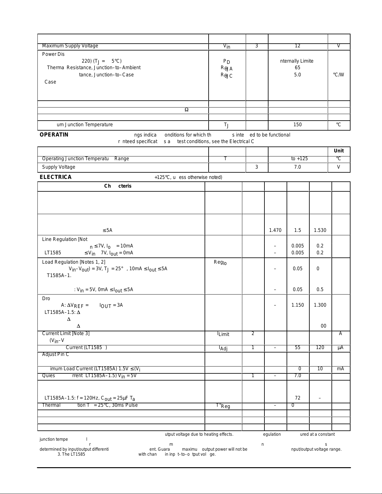
Figure 1. Dropout Voltage vs Output Current
1.4
1.3
1.2
1.1
1.0
0.9
0.8
DROPOUT VOLTAGE (V)
0.7
0.6
0.5
0 2.0 6.0
1.0 3.0 5.0
OUTPUT CURRENT (A)
–5°C
25°C
125°C
4.0
Figure 3. Load Regulation vs T emperature
0.1
0.05
0
–0.05
–0.1
LOAD REGULATION (%)
–0.15
–0.2
–40–60 20
0–20 60 80 140120
40 100
TEMPERATURE (
°
C)
Figure 2. Short–Circuit Current vs Temperature
7.0
6.8
6.6
6.4
6.2
(A)
6.0
sc
I
5.8
5.6
5.4
5.2
5.0
–40–60 20 140
0–20 60 80 120
40 100
TEMPERATURE (
°
C)
Figure 4. L T1585A Reference Voltage vs
T emperature
1.275
1.27
1.265
1.26
1.255
(V)
1.25
ref
V
1.245
1.24
1.235
1.23
1.225
–40–60 20 160
0–20 60 80 140120
40 100
TEMPERATURE (
°
C)
Figure 5. L T1585A–1.5 Output Voltage vs
T emperature
1.515
1.51
1.505
(V)
1.5
out
V
1.495
1.49
1.485
–40–60 20
0–20 60 80 140120
40 100
TEMPERATURE (
°
C)
MOTOROLA ANALOG IC DEVICE DATA
Figure 6. L T1585A–1.5 Quiescent Current vs
T emperature
10
9.5
9.0
8.5
8.0
(mA)
7.5
q
I
7.0
6.5
6.0
5.5
5.0
–40–60 20
0–20 60 80 140120
40 100
TEMPERATURE (
°
C)
3
LT1585A
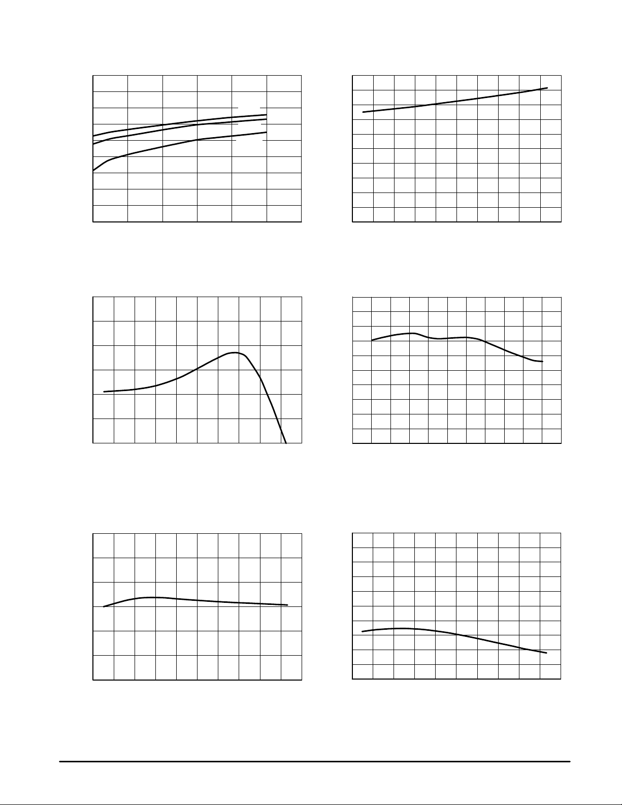
Figure 7. L T1585A Adjust Pin Current vs
T emperature
0–20 60 80 140120
40 100
TEMPERATURE (
°
C)
m
( A)
adj
I
100
90
80
70
60
50
40
30
20
10
0
–40–60 20 160
OPERA TING DESCRIPTION
APPLICATIONS INFORMATION
General
The LT1585A 3–terminal adjustable positive voltage
regulator is easy to use and has all the protection features
expected in high performance linear regulators. The device is
short–circuit protected, safe–area protected and provides
thermal shutdown to turn off the regulator should the junction
temperature exceed about 150°C.
The LT1585A voltage regulator requires an output
capacitor for stability. However, the improved frequency
compensation permits the use of capacitors with much lower
ESR while still maintaining stability. This is critical in
addressing the needs of modern, low voltage, high speed
microprocessors.
Current generation microprocessors cycle load current
from almost zero to amps in tens of nanoseconds. Output
voltage tolerances are tighter and include transient response
as part of the specification.
The LT1585A is specifically designed to meet the fast
current load–step requirements of these microprocessors
and save total cost by needing less output capacitance in
order to maintain regulation.
Stability
The circuit design in the LT1585A requires the use of an
output capacitor as part of the frequency compensation. For
all operating conditions, the addition of a 22µF solid tantalum
or a 100µF aluminium electrolytic on the output ensures
stability. Normally, the LT1585A can use smaller value
capacitors. Many different types of capacitors are available
and have widely varying characteristics.
These capacitors differ in capacitor tolerance (sometimes
ranging up to ±100%), equivalent series resistance,
equivalent series inductance and capacitance temperature
coefficient. The L T1585A frequency compensation optimizes
frequency response with low ESR capacitors. In general, use
capacitors with an ESR of less than 1 Ω.
On the L T1585A, bypassing the adjust pin improves ripple
rejection and transient response. Bypassing the adjust pin
increases the required output capacitor value. The value of
22µF tantalum or 100µF aluminium covers all cases of
Figure 8. Ripple Rejection vs Frequency
90
80
70
60
50
(V)
ref
40
V
30
20
10
0
10 100,000
100 1000
TEMPERATURE (
10,000
°
C)
bypassing the adjust terminal. With no adjust pin bypassing,
smaller values of capacitors provide equally good results.
Normally , capacitor values on the order of several hundred
microfarads are used on the output of the regulators to
ensure good transient response with heavy load current
changes.
Output capacitance can increase without limit and larger
values of output capacitance further improve the stability and
transient response of the L T1585A.
Large load current changes are exactly the situation
presented by modern microprocessors. The load current step
contains higher order frequency components that the output
decoupling network must handle until the regulator throttles
to the load current level. Capacitors are not ideal elements
and contain parasitic resistance and inductance. These
parasitic elements dominate the change in output voltage at
the beginning of a transient load step change.
The ESR of the output capacitors produces an
instantaneous step in output voltage (∆V = ∆I • ESR). The
ESL of the output capacitors produces a droop proportional
to the rate of change of output current (V = L• ∆I/∆t). The
output capacitance produces a change in output voltage
proportional to the time until the regulator can respond (∆V =
∆t • ∆l/C). These transient effects are illustrated in Figure 9.
Figure 9.
ESR
Effects
ESL
Effects
Slope,
V
D
I
+
t
C
Point at which
Regulator Takes Control
Capacitance
Effects
4
MOTOROLA ANALOG IC DEVICE DATA

LT1585A
The use of capacitors with low ESR, low ESL and good
high frequency characteristics is critical in meeting the output
voltage tolerances of these high speed microprocessors.
These requirements dictate a combination of high quality,
surface mount tantalum capacitors and ceramic capacitors.
The location of the decoupling network is critical to
transient response performance. Place the decoupling
network as close as possible to the processor pins because
trace runs from the decoupling capacitors to the processor
pins are inductive. The ideal location for the decoupling
network is actually inside the microprocessor socket cavity.
In addition, use large power and ground plane areas to
minimize distribution drops.
A possible stability problem that occurs in monolithic linear
regulators is current limit oscillations. The LT1585A
essentially has a flat current limit over the range of input
supply voltage. The lower current limit rating and 12V
maximum supply voltage rating for these devices permit this
characteristic.
Current limit oscillations are typically nonexistent, unless
the input and output decoupling capacitors for the regulators
are mounted several inches from the terminals.
Protection Diodes
In normal operation, the LT1585A does not require any
protection diodes. Older 3–terminal regulators require
protection diodes between the output pin and the input pin or
between the adjust pin and the output pin to prevent die
overstress.
Built–in internal resistors limit internal current paths on the
adjust pin. Therefore, even with bypass capacitors on the
adjust pin, no protection diode is needed to ensure device
safety under short–circuit conditions.
A protection diode between the input and output pins is
usually not needed. An internal diode between the input and
output pins on the LT1585A can handle microsecond surge
currents of 50A to 100A. Even with large value output
capacitors it is difficult to obtain those values of surge
currents in normal operation. Only with large values of output
capacitance, such as 1000µF to 500µF , and with the input pin
instantaneously shorted to ground can damage occur. A
crowbar circuit at the input of the LT1585A can generate
those levels of current, and a diode from output to input is
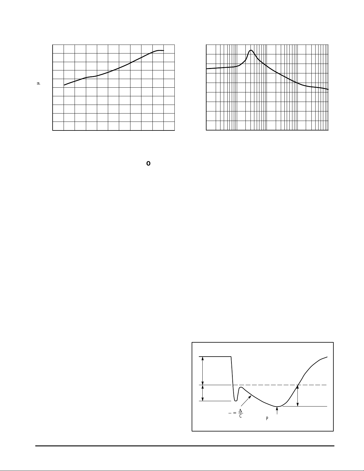
then recommended. This is shown in Figure 10. Usually,
normal power supply cycling or system “hot plugging and
unplugging” will not generate current large enough to do any
damage.
The adjust pin can be driven on a transient basis ± 7V with
respect to the output, without any device degradation. As
with any IC regulator, exceeding the maximum
input–to–output voltage differential causes the internal
transistors to break down and none of the protection circuitry
is then functional.
Figure 10.
D1
1N4002
(Optional)
LT1585A
V
in
C1
m
F
10
IN OUT
+
ADJ
+
R1
C
R2
V
C2
10
out
m
F
+
Ripple Rejection
A bypass capacitor from the adjust pin to ground reduces
the output ripple by the ratio of V
/1.25 V . The impedance
OUT
of the adjust pin capacitor at the ripple frequency should be
less than the value of R1 (typically in the rage of 100Ω to
120Ω) in the feedback divider network in Figure 10.
Therefore, the value of the required adjust pin capacitor is a
function of the input ripple frequency. For example, if R1
equals 100Ω and the ripple frequency equals 120Hz, the
adjust pin capacitor should be 22µF . At 10kHz, only 0.22µF is
needed.
Output Voltage
The LT1585A adjustable regulator develops a 1.25V
reference voltage between the output pin and the adjust pin
(see Figure 11). Placing a resistor R1 between these two
terminals causes a constant current to flow through R1 and
down through R2 to set the overall output voltage. Normally,
this current is the specified minimum load current of 10mA.
The current out of the adjust pin adds to the current from R1
and is typically 55µA. Its output voltage contribution is small
and only needs consideration when very precise output
voltage setting is required.
MOTOROLA ANALOG IC DEVICE DATA
5

LT1585A
Figure 11. Basic Adjustable Regulator
LT1585A
V
in
C1
m
F
10
V
= V
(1 + R2/R1) + I
out
ref
IN OUT
+
I
adj
55
adj
ADJ
m
A
(R2)
V
ref
R1
R2
Load Regulation
It is not possible to provide true remote load sensing
because the LT1585A are 3–terminal devices. Load
regulation is limited by the resistance of the wire connecting
the regulators to the load. Load regulation per the data sheet
specification is measured at the bottom of the package.
For adjustable voltage devices, negative side sensing is a
true Kelvin connection with the bottom of the output divider
returned to the negative side of the load. The best load
regulation is obtained when the top of resistor divider R1
connects directly to the regulator output and not to the load.
Figure 4 illustrates this point. If R1 connects to the load, the
effective resistance between the regulator and the load is :
R
(1 + R2/R1), RP = Parasitic Line Resistance
P
The connection shown in Figure 11 does not multiply R
by the divider ratio. As an example, R
is about four milliohms
P
per foot with 16–gauge wire. This translates to 4mV per foot
at 1A load current. At higher load currents, this drop
represents a significant percentage of the overall regulation.
It is important to keep the positive lead between the regulator
and the load as short as possible and to use large wire or PC
board traces.
Figure 12. Connection for
Best Load Regulation
P
D
LT1585A
V
in
IN OUT
ADJ
* Connect R1 to Case
* Connect R2 to Load
Parasitic
Line Resistance
R1*
R2*
V
C2
10
out
m
F
FL
+
Thermal Considerations
The LT1585A protects the device under overload
conditions with internal power and thermal limiting circuitry.
However, for normal continuous load conditions, do not
exceed maximum junction temperature ratings. It is important
to consider all sources of thermal resistance from
junction–to–ambient. These sources include the
junction–to–case resistance, the case–to–heat sink interface
resistance and the heat sink resistance. Thermal resistance
specifications have been developed to more accurately
reflect device temperature and ensure safe operating
temperatures. The Electrical Characteristics section provides
a separate thermal resistance and maximum junction
temperature for both the control circuitry and the power
transistor. Older regulators, with a single junction–to–case
thermal resistance specification, use an average of the two
values provided here and allow excessive junction
temperatures under certain conditions of ambient
temperature and heat sink resistance.
Calculate the maximum junction temperature for both
sections to ensure that both thermal limits are met.
Junction–to–case thermal resistance is specified from the
IC junction to the bottom of the case directly below the
die.This is the lowest resistance path for heat flow. Proper
mounting ensures the best thermal flow from this area of the
package to the heat sink. It is strongly recommended to use
thermal compound at the case–to–heat sink interface. Use a
thermally conductive spacer if the case of the device must be
electrically isolated and include its contribution to the total
thermal resistance.
P
For example, using an LT1585ACT (TO–220 package)
with an output adjusted to 3.3 V and assuming:
V
(Max Continuous) = 5.25V (5V + 5%), V
in
TJ I
T
q
= 5A.
OUT
= 70°C,
A
q
HEA T SINK
CASE–TO–HEA T SINK
= 3°C/W
= 1°C/W (with Thermal Compound)
out
= 3.3V,
Power dissipation under these conditions is equal to:
P
= (Vin – V
D
out
) (I
) = (5.25 – 3.3) (5) = 9.75W
out
Junction temperature will be equal to:
= TA + PD (
T
J
q
HEA T SINK
+
q
CASE–TO–HEA T SINK
+
qJC)
For the Control Section:
T
= 70°C + 9.75W (3°C/W + 1°C/W + 0.7°C/W)
J
T
= 115.8°C
J
1 15.8°C < 125°C = T
JMAX
(Control Section Commercial Range)
For the Power Transistor:
T
= 70°C + 9.75W (3°C/W + 1°C/W + 3°C/W)
J
T
= 138.3°C
J
138.3°C < 150°C = T
JMAX
(Control Section Commercial Range)
In both cases the junction temperature is below the
maximum rating for the respective sections, ensuring reliable
operation.
6
MOTOROLA ANALOG IC DEVICE DATA
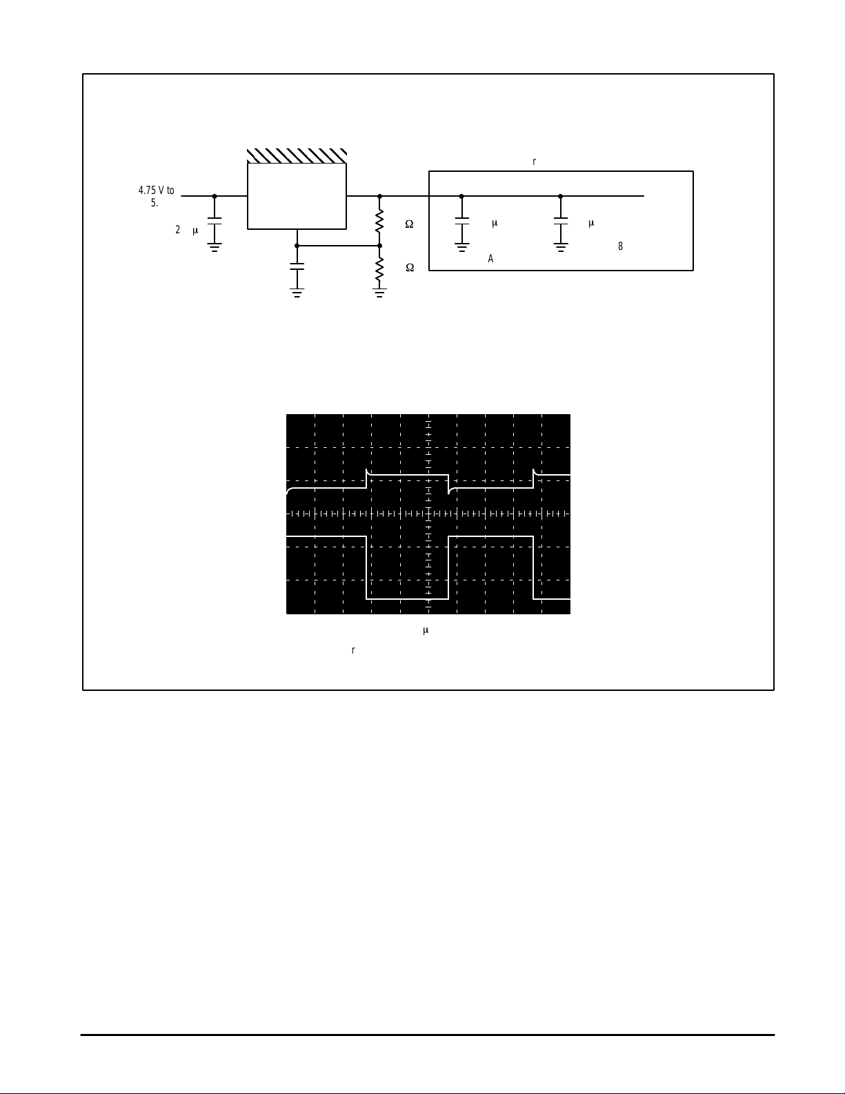
4.75 V to
5.25 V
C1 to C3
AVX TPS
LT1585A
Minimum Parts Count LT1585A Adjustable Circuit for the Intel 120 MHz Pentium Processor
Thermalloy
7020B–MT
Place in Microprocessor Socket Cavity
LT1585ACT
m
F
220
10 V
3 EACH
IN OUT
+
330 nF
AVX X7R0805
C5 to C10
ADJ
C4
16 V
LT1585A T ransient Response for 3.8 A Load Current Step*
R1
110
0.1%
R2
197
0.1%
W
W
+
m
F
100
10 V
AVX TPS
4 EACH
AVX Corp. (803) 448–9411
Thermalloy Inc. (214) 243–4321
Do not substitute components
C11 to C20
+
m
1.0
16 V
AVX V5 V0805
24 EACH
F
350 V
5 A
V
out
50 mV/DIV
I
out
2 A/DIV
100
m
s/DIV
* transient response measured with an Intel power validator.
* V
is measured at the power validator.
out
MOTOROLA ANALOG IC DEVICE DATA
7

LT1585A
OUTLINE DIMENSIONS
T SUFFIX
PLASTIC PACKAGE
CASE 221A–09
ISSUE Z
SEATING
–T–
PLANE
T
4
Q
123
A
U
C
S
H
K
Z
L
V
R
J
G
D
N
NOTES:
1. DIMENSIONING AND TOLERANCING PER ANSI
Y14.5M, 1982.
2. CONTROLLING DIMENSION: INCH.
3. DIMENSION Z DEFINES A ZONE WHERE ALL
BODY AND LEAD IRREGULARITIES ARE
ALLOWED.
DIM MIN MAX MIN MAX
A 0.570 0.620 14.48 15.75
B 0.380 0.405 9.66 10.28
C 0.160 0.190 4.07 4.82
D 0.025 0.035 0.64 0.88
F 0.142 0.147 3.61 3.73
G 0.095 0.105 2.42 2.66
H 0.110 0.155 2.80 3.93
J 0.018 0.025 0.46 0.64
K 0.500 0.562 12.70 14.27
L 0.045 0.060 1.15 1.52
N 0.190 0.210 4.83 5.33
Q 0.100 0.120 2.54 3.04
R 0.080 0.110 2.04 2.79
S 0.045 0.055 1.15 1.39
T 0.235 0.255 5.97 6.47
U 0.000 0.050 0.00 1.27
V 0.045 ––– 1.15 –––
Z ––– 0.080 ––– 2.04
MILLIMETERSINCHES
K
B
F
J
D
0.010 (0.254) T
M
C
A
S
123
G
OPTIONAL
CHAMFER
H
PLASTIC PACKAGE
–T–
N
R
CM SUFFIX
CASE 936–03
ISSUE B
(D2PAK)
E
V
M
L
TERMINAL 4
U
P
NOTES:
1. DIMENSIONING AND TOLERANCING PER ANSI
Y14.5M, 1982.
2. CONTROLLING DIMENSION: INCH.
3. TAB CONTOUR OPTIONAL WITHIN DIMENSIONS
A AND K.
4. DIMENSIONS U AND V ESTABLISH A MINIMUM
MOUNTING SURFACE FOR TERMINAL 4.
5. DIMENSIONS A AND B DO NOT INCLUDE MOLD
FLASH OR GATE PROTRUSIONS. MOLD FLASH
AND GATE PROTRUSIONS NOT TO EXCEED
0.025 (0.635) MAXIMUM.
INCHES
DIMAMIN MAX MIN MAX
0.386 0.403 9.804 10.236
B 0.356 0.368 9.042 9.347
C 0.170 0.180 4.318 4.572
D 0.026 0.036 0.660 0.914
E 0.045 0.055 1.143 1.397
F 0.051 REF 1.295 REF
G 0.100 BSC 2.540 BSC
H 0.539 0.579 13.691 14.707
J 0.125 MAX 3.175 MAX
K 0.050 REF 1.270 REF
L 0.000 0.010 0.000 0.254
M 0.088 0.102 2.235 2.591
N 0.018 0.026 0.457 0.660
P 0.058 0.078 1.473 1.981
__
R
S 0.116 REF 2.946 REF
U 0.200 MIN 5.080 MIN
V 0.250 MIN 6.350 MIN
MILLIMETERS
5 REF5 REF
8
MOTOROLA ANALOG IC DEVICE DATA

LT1585A
Motorola reserves the right to make changes without further notice to any products herein. Motorola makes no warranty , representation or guarantee regarding
the suitability of its products for any particular purpose, nor does Motorola assume any liability arising out of the application or use of any product or circuit, and
specifically disclaims any and all liability, including without limitation consequential or incidental damages. “T ypical” parameters which may be provided in Motorola
data sheets and/or specifications can and do vary in different applications and actual performance may vary over time. All operating parameters, including “Typicals”
must be validated for each customer application by customer’s technical experts. Motorola does not convey any license under its patent rights nor the rights of
others. Motorola products are not designed, intended, or authorized for use as components in systems intended for surgical implant into the body, or other
applications intended to support or sustain life, or for any other application in which the failure of the Motorola product could create a situation where personal injury
or death may occur. Should Buyer purchase or use Motorola products for any such unintended or unauthorized application, Buyer shall indemnify and hold Motorola
and its officers, employees, subsidiaries, affiliates, and distributors harmless against all claims, costs, damages, and expenses, and reasonable attorney fees
arising out of, directly or indirectly, any claim of personal injury or death associated with such unintended or unauthorized use, even if such claim alleges that
Motorola was negligent regarding the design or manufacture of the part. Motorola and are registered trademarks of Motorola, Inc. Motorola, Inc. is an Equal
Opportunity/Affirmative Action Employer.
How to reach us:
USA/EUROPE/Locations Not Listed: Motorola Literature Distribution; JAPAN: Motorola Japan Ltd.; SPD, Strategic Planning Office, 141,
P.O. Box 5405, Denver, Colorado 80217. 1–303–675–2140 or 1–800–441–2447 4–32–1 Nishi–Gotanda, Shinagawa–ku, Tokyo, Japan. 81–3–5487–8488
Customer Focus Center: 1–800–521–6274
Mfax: RMFAX0@email.sps.mot.com – TOUCHTONE 1–602–244–6609 ASIA/PACIFIC: Motorola Semiconductors H.K. Ltd.; Silicon Harbour Centre,
Motorola Fax Back System – US & Canada ONLY 1–800–774–1848 2, Dai King Street, T ai Po Industrial Estate, Tai Po, N.T., Hong Kong.
HOME PAGE: http://motorola.com/sps/
MOTOROLA ANALOG IC DEVICE DATA
– http://sps.motorola.com/mfax/ 852–26629298
◊
Mfax is a trademark of Motorola, Inc.
LT1585A/D
9
 Loading...