

查询LP2950/D供应商
Order this document by LP2950/D
The LP2950 and LP2951 are micropower voltage regulators that are
specifically designed to maintain proper regulation with an extremely low
input–to–output voltage differential. These devices feature a very low
quiescent bias current of 75 µA and are capable of supplying output currents
in excess of 100 mA. Internal current and thermal limiting protection is
provided.
The LP2951 has three additional features. The first is the Error
that can be used to signal external circuitry of an out of regulation condition,
or as a microprocessor power–on reset. The second feature allows the
output voltage to be preset to 5.0 V, 3.3 V or 3.0 V output (depending on the
version) or programmed from 1.25 V to 29 V. It consists of a pinned out
resistor divider along with direct access to the Error Amplifier feedback input.
The third feature is a Shutdown input that allows a logic level signal to
turn–off or turn–on the regulator output.
Due to the low input–to–output voltage differential and bias current
specifications, these devices are ideally suited for battery powered
computer, consumer, and industrial equipment where an extension of
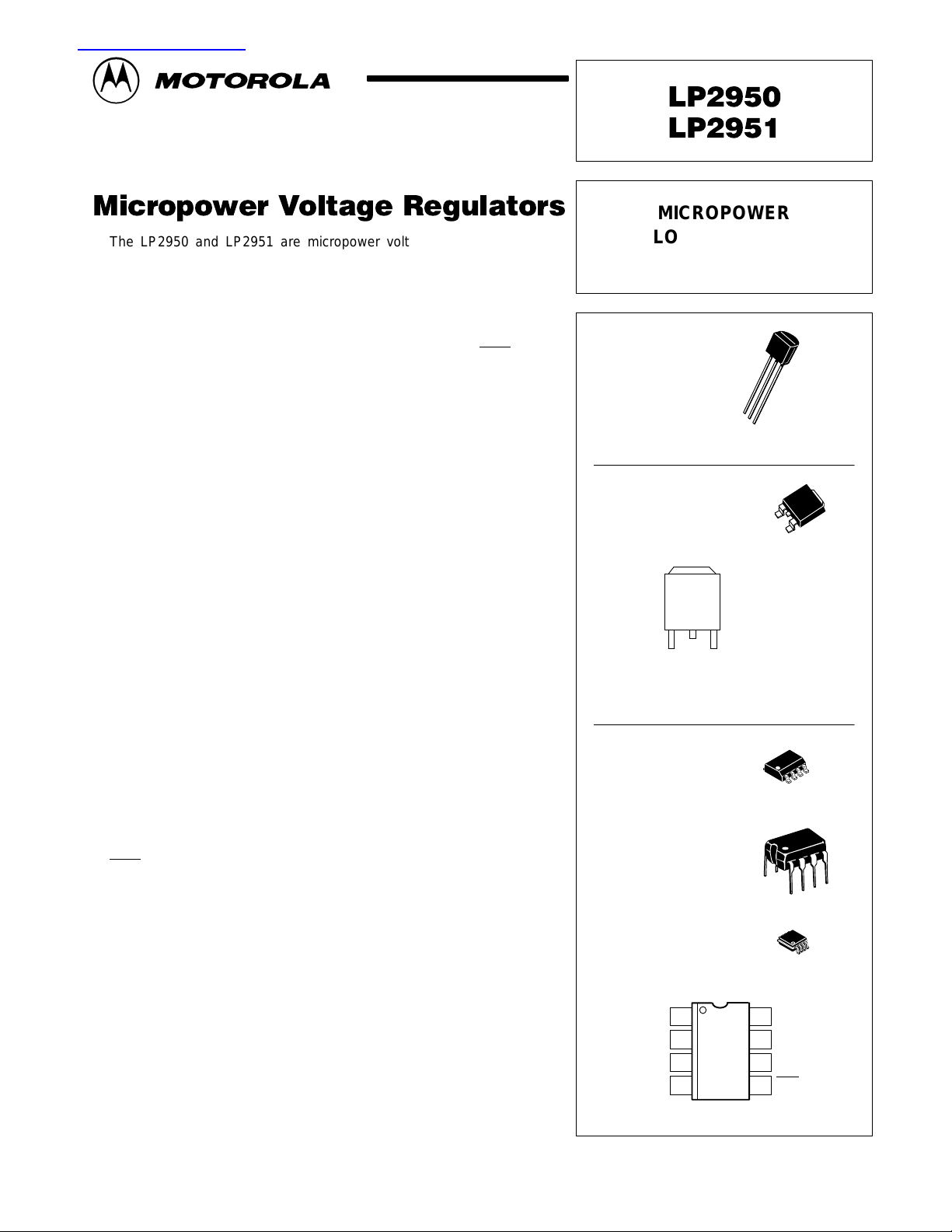
useful battery life is desirable. The LP2950 is available in the three pin case
29 and DPAK packages, and the LP2951 is available in the eight pin
dual–in–line, SO–8 and Micro–8 surface mount packages. The ‘A’ suffix
devices feature an initial output voltage tolerance ±0.5%.
LP2950 and LP2951 Features:
• Low Quiescent Bias Current of 75 µA
• Low Input–to–Output Voltage Differential of 50 mV at 100 µA and
380 mV at 100 mA
• 5.0 V, 3.3 V or 3.0 V ±0.5% Allows Use as a Regulator or Reference
• Extremely Tight Line and Load Regulation
• Requires Only a 1.0 µF Output Capacitor for Stability
• Internal Current and Thermal Limiting
Output
MICROPOWER
LOW DROPOUT
VOLTAGE REGULATORS
Z SUFFIX
PLASTIC PACKAGE
CASE 29
(TO–226AA/TO–92)
DT SUFFIX
PLASTIC PACKAGE
CASE 369A
(DPAK)
123
(Top View)
Heatsink surface (shown as terminal 4 in
case outline drawing) is connected to Pin 2.
D SUFFIX
PLASTIC PACKAGE
CASE 751
(SO–8)
1
2
3
1
Pin: 1. Input
2. Ground
3. Output
8
Pin: 1. Output
2. Ground
3. Input
3
1
LP2951 Additional Features:
• Error Output Signals an Out of Regulation Condition
• Output Programmable from 1.25 V to 29 V
• Logic Level Shutdown Input
(See Following Page for Ordering Information.)
MOTOROLA ANALOG IC DEVICE DATA
N SUFFIX
PLASTIC PACKAGE
CASE 626
DM SUFFIX
PLASTIC PACKAGE
CASE 846A
(Micro–8)
18
Output
2
Sense
Shutdown
Motorola, Inc. 1996 Rev 4
3
4
Gnd
(Top View)
8
1
8
1
Input
7
Feedback
6
VO Tap
5
Error Output
1
LP2950 LP2951
Fixed Voltage
(
)
LP2950CDT–**
(3.0, 3.3 or 5.0 V)
LP2950ACDT–**
DPAK
LP2951CD–**
Adjustable or Fixed
LP2951ACD–**
(3.0, 3.3 V)
T
40° t
125°C
LP2951CN–**
Adjustable or Fixed
LP2951ACN–**
(3.0, 3.3 V)
LP2951CDM–**
Adjustable or Fixed
LP2951ACDM–**
(3.0, 3.3 V)
ORDERING INFORMATION
Operating
Device Type
LP2950CZ–**
LP2950ACZ–**
–**
**
LP2951CD
LP2951ACD
–**
**
LP2951CN
LP2951ACN
–**
**
LP2951CDM
LP2951ACDM
–**
**
** = Voltage option of 3.0, 3.3 or 5.0 V.
Fixed Voltage
3.0, 3.3 or 5.0 V
Adjustable or
5.0 V Fixed
Adjustable or
5.0 V Fixed
Adjustable or
5.0 V Fixed
DEVICE TYPE/NOMINAL OUTPUT VOLTAGE
Device No. (±1%) Device No. (±0.5%) Nominal Voltage
LP2950CX–5.0 LP2950ACX–5.0 5.0
LP2950CX–3.3 LP2950ACX–3.3 3.3
LP2950CX–3.0 LP2950ACX–3.0 3.0
LP2951CX LP2951ACX Adjustable or 5.0
LP2950CX–3.3 LP2951ACX–3.3 Adjustable or 3.3
LP2951CX–3.0 LP2951ACX–3.0 Adjustable or 3.0
X = Package suffix.
Battery or
Unregulated DC
Temperature Range
TO–92/TO–226AA
J
= –
°
o +
°
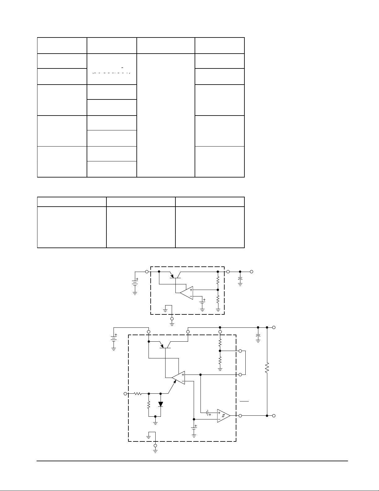
Representative Block Diagrams
Input
3
Package
DPAK
SO–8
Plastic
Micro–8
182 k
Output
1
5.0 V/100 mA
µ
F
1.0
Error Amplifier
1.23 V
Reference
Gnd 2
Battery or
Unregulated DC
Shutdown
From
CMOS/TTL
Input 8 Output
Amplifier
3
60 k
50 k
Gnd 4
Error
1.23 V
Reference
2
60 k
Sense 2
1
182 k
75 mV/
60 mV
Error Detection
Comparator
LP2950CZ–5.0
5.0 V/100 mA
1.0 µF
VO Tap
60 k
This device contains 34 active transistors.
6
7
Feedback
Error
Output
5
LP2951CD or CN
330 k
To CMOS/TTL
MOTOROLA ANALOG IC DEVICE DATA
LP2950 LP2951
БББББ
БББББ
БББББ
БББББ
БББББ
БББББ
БББББ
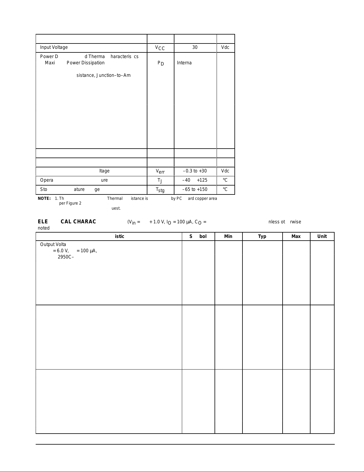
MAXIMUM RATINGS (T
= 25°C, unless otherwise noted.)
A
Rating Symbol Value Unit
Input Voltage
V
CC
30
Power Dissipation and Thermal Characteristics
Maximum Power Dissipation P
Internally Limited W
D
Case 751(SO–8) D Suffix
Thermal Resistance, Junction–to–Ambient R
Thermal Resistance, Junction–to–Case R
θJA
θJC
180 °C/W
45 °C/W
Case 369A (DPAK) DT Suffix [Note 1]
Thermal Resistance, Junction–to–Ambient R
Thermal Resistance, Junction–to–Case R
θJA
θJC
92 °C/W
6.0 °C/W
Case 29 (TO–226AA/TO–92) Z Suffix
Thermal Resistance, Junction–to–Ambient R
Thermal Resistance, Junction–to–Case R
θJA
θJC
160 °C/W
83 °C/W
Case 626 N Suffix
Thermal Resistance, Junction–to–Ambient R
θJA
105 °C/W
Case 846A (Micro–8) DM Suffix
Thermal Resistance, Junction–to–Ambient R
Feedback Input Voltage
Shutdown Input Voltage
Error Comparator Output Voltage
Operating Junction Temperature
Storage Temperature Range
NOTE: 1.The Junction–to–Ambient Thermal Resistance is determined by PC board copper area
per Figure 26.
2.ESD data available upon request.
V
V
V
T
θJA
fb
sd
err
T
J
stg
240 °C/W
–1.5 to +30
–0.3 to +30
–0.3 to +30
–40 to +125
–65 to +150
Vdc
Vdc
Vdc
Vdc
°C
°C
ELECTRICAL CHARACTERISTICS (V
= VO + 1.0 V, IO = 100 µA, CO = 1.0 µF, TJ = 25°C [Note 1], unless otherwise
in
noted.)
Characteristic
Output Voltage, 5.0 V Versions V
Symbol Min Typ Max Unit
O
Vin = 6.0 V, IO = 100 µA, TJ = 25°C
LP2950C–5.0/LP2951C 4.950 5.000 5.050
LP2950AC–5.0/LP2951AC 4.975 5.000 5.025
TJ = –40 to +125°C
LP2950C–5.0/LP2951C 4.900 – 5.100
LP2950AC–5.0/LP2951AC 4.940 – 5.060
Vin = 6.0 to 30 V, IO = 100 µA to 100 mA, TJ = –40 to +125°C
LP2950C–5.0/LP2951C 4.880 – 5.120
LP2950AC–5.0/LP2951AC 4.925 – 5.075
Output Voltage, 3.3 V Versions V
O
Vin = 4.3 V, IO = 100 µA, TJ = 25°C
LP2950C–3.3/LP2951C–3.3 3.267 3.300 3.333
LP2950AC–3.3/LP2951AC–3.3 3.284 3.300 3.317
TJ = –40 to +125°C
LP2950C–3.3/LP2951C–3.3 3.234 – 3.366
LP2950AC–3.3/LP2951AC–3.3 3.260 – 3.340
Vin = 4.3 to 30 V, IO = 100 µA to 100 mA, TJ = –40 to +125°C
LP2950C–3.3/LP2951C–3.3 3.221 – 3.379
LP2950AC–3.3/LP2951AC–3.3 3.254 – 3.346
Output Voltage, 3.0 V Versions V
O
Vin = 4.0 V, IO = 100 µA, TJ = 25°C
LP2950C–3.0/LP2951C–3.0 2.970 3.000 3.030
LP2950AC–3.0/LP2951AC–3.0 2.985 3.000 3.015
TJ = –40 to +125°C
LP2950C–3.0/LP2951C–3.0 2.940 – 3.060
LP2950AC–3.0/LP2951AC–3.0 2.964 – 3.036
Vin = 4.0 to 30 V, IO = 100 µA to 100 mA, TJ = –40 to +125°C
LP2950C–3.0/LP2951C–3.0 2.928 – 3.072
LP2950AC–3.0/LP2951AC–3.0 2.958 – 3.042
V
V
V
MOTOROLA ANALOG IC DEVICE DATA
3
LP2950 LP2951
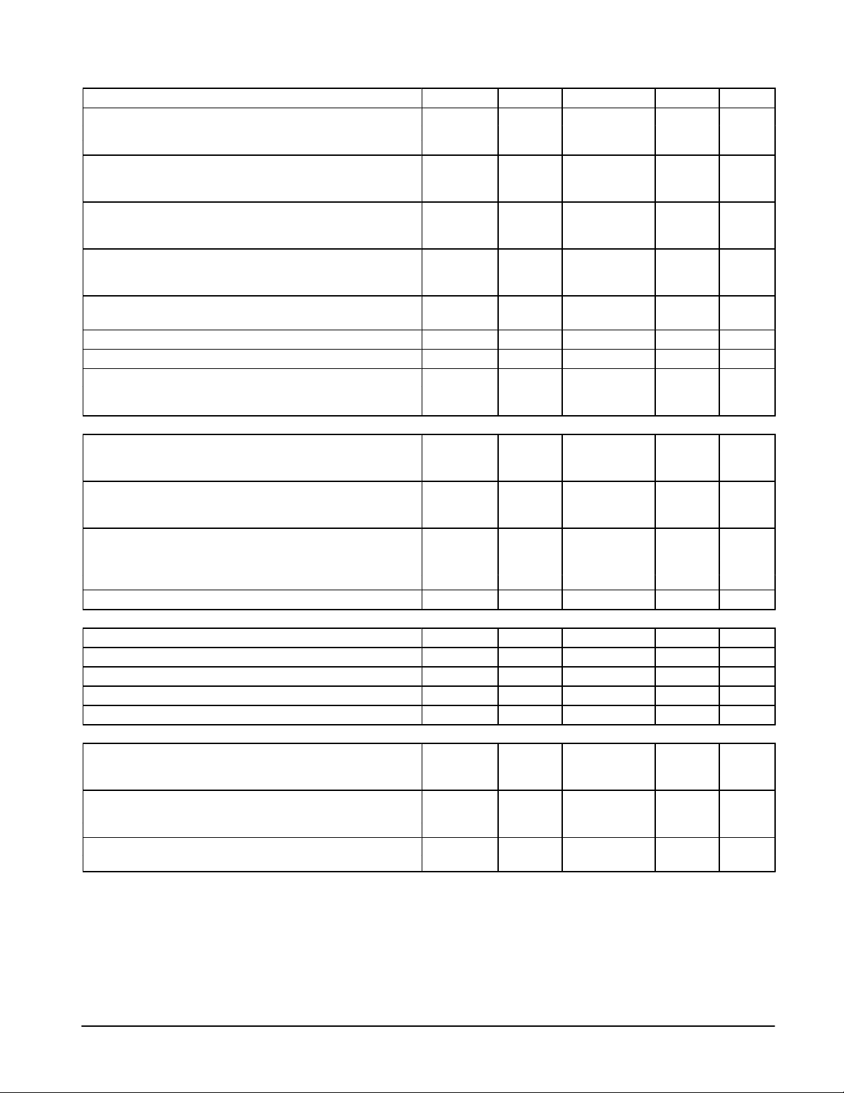
ELECTRICAL CHARACTERISTICS (continued)
noted.)
Characteristic UnitMaxTypMinSymbol
Line Regulation (Vin = V
LP2950C–XX/LP2951C/LP2951C–XX – 0.08 0.20
LP2950AC–XX/LP2951AC/LP2951AC–XX – 0.04 0.10
Load Regulation (IO = 100 µA to 100 mA) Reg
LP2950C–XX/LP2951C/LP2951C–XX – 0.13 0.20
LP2950AC–XX/LP2951AC/LP2951AC–XX – 0.05 0.10
Dropout Voltage VI – V
IO = 100 µA – 30 80
IO = 100 mA – 350 450
Supply Bias Current I
IO = 100 µA – 93 120 µA
IO = 100 mA – 4.0 12 mA
Dropout Supply Bias Current (Vin = V
IO = 100 µA) [Note 2]
Current Limit (VO Shorted to Ground) I
Thermal Regulation Reg
Output Noise Voltage (10 Hz to 100 kHz) [Note 3] V
CL = 1.0 µF – 126 –
CL = 100 µF – 56 –
LP2951A/LP2951AC ONL Y
Reference Voltage (TJ = 25°C) V
LP2951C/LP2951C–XX 1.210 1.235 1.260
LP2951AC/LP2951AC–XX 1.220 1.235 1.250
Reference Voltage (TJ = –40 to +125°C) V
LP2951C/LP2951C–XX 1.200 – 1.270
LP2951AC/LP2951AC–XX 1.200 – 1.260
Reference Voltage (TJ = –40 to +125°C) V
IO = 100 µA to 100 mA, Vin = 23 to 30 V
LP2951C/LP2951C–XX 1.185 – 1.285
LP2951AC/LP2951AC–XX 1.190 – 1.270
Feedback Pin Bias Current I
ERROR COMPARATOR
Output Leakage Current (VOH = 30 V) I
Output Low Voltage (Vin = 4.5 V, IOL = 400 µA) V
Upper Threshold Voltage (Vin = 6.0 V) V
Lower Threshold Voltage (Vin = 6.0 V) V
Hysteresis (Vin = 6.0 V) V
SHUTDOWN INPUT
Input Logic Voltage V
Logic “0” (Regulator “On”) 0 – 0.7
Logic “1” (Regulator “Off”) 2.0 – 30
Shutdown Pin Input Current I
V
= 2.4 V – 35 50
shtdn
V
= 30 V – 450 600
shtdn
Regulator Output Current in Shutdown Mode I
(Vin = 30 V, V
NOTES: 1. Low duty pulse techniques are used during test to maintain junction temperature as close to ambient as possible.
2.V
O(nom)
3.
Noise tests on the LP2951 are made with a 0.01 µF capacitor connected across Pins 7 and 1.
= 2.0 V, VO = 0, Pin 6 Connected to Pin 7)
shtdn
is the part number voltage option.
+1.0 V to 30 V) [Note 2] Reg
O(nom)
– 0.5 V,
O(nom)
(Vin = VO + 1.0 V, IO = 100 µA, CO = 1.0 µF, TJ = 25°C [Note 1], unless otherwise
line
load
O
CC
I
CCdropout
Limit
thermal
n
ref
ref
ref
FB
lkg
OL
thu
thl
hy
shtdn
shtdn
off
– 110 170 µA
– 220 300 mA
– 0.05 0.20 %/W
– 15 40 nA
– 0.01 1.0 µA
– 150 250 mV
40 45 – mV
– 60 95 mV
– 15 – mV
– 3.0 10 µA
%
%
mV
µVrms
V
V
V
V
µA
4
MOTOROLA ANALOG IC DEVICE DATA
LP2950 LP2951
DEFINITIONS
Dropout V oltage – The input/output voltage dif ferential at
which the regulator output no longer maintains regulation
against further reductions in input voltage. Measured when
the output drops 100 mV below its nominal value (which is
measured at 1.0 V differential), dropout voltage is affected by
junction temperature, load current and minimum input supply
requirements.
Line Regulation – The change in output voltage for a
change in input voltage. The measurement is made under
conditions of low dissipation or by using pulse techniques
such that average chip temperature is not significantly
affected.
Load Regulation – The change in output voltage for a
change in load current at constant chip temperature.
Maximum Power Dissipation – The maximum total
device dissipation for which the regulator will operate within
specifications.
Bias Current – Current which is used to operate the
regulator chip and is not delivered to the load.
Figure 1. Quiescent Current
10
1.0
Output Noise V oltage – The rms ac voltage at the output,
with constant load and no input ripple, measured over a
specified frequency range.
Leakage Current – Current drawn through a bipolar
transistor collector–base junction, under a specified collector
voltage, when the transistor is “off”.
Upper Threshold Voltage – Voltage applied to the
comparator input terminal, below the reference voltage
which is applied to the other comparator input terminal,
which causes the comparator output to change state from a
logic “0” to “1”.
Lower Threshold Voltage – Voltage applied to the
comparator input terminal, below the reference voltage
which is applied to the other comparator input terminal,
which causes the comparator output to change state from a
logic “1” to “0”.
Hysteresis – The difference between Lower Threshold
voltage and Upper Threshold voltage.
Figure 2. Dropout Characteristics
6.0
LP2951C
5.0
4.0
TA = 25
°
C
RL = 50 k
0.1
LP2950/LP2951 BIAS CURRENT (mA)
0.01
250
200
µ
150
100
BIAS CURRENT ( A)
50
0.1
0
3.0
RL = 50
2.0
, OUTPUT VOL TAGE (V)
out
1.0
V
1.0 10 100 1.0 2.0 3.0 4.0 5.0 6.0
IL, LOAD CURRENT (mA)
0
0
Vin, INPUT VOLTAGE (V)
Ω
Figure 3. Input Current Figure 4. Output Voltage versus Temperature
5.00
, OUTPUT VOL TAGE (V)
V
out
4.99
4.98
4.97
4.96
4.95
–50
TA, AMBIENT TEMPERATURE (
°
C)
LP2951C
0.1 mA Load Current
No Load
0
5.0 10 15 20 25 0 50 100 150
Vin, INPUT VOLTAGE (V)
MOTOROLA ANALOG IC DEVICE DATA
5

400
350
300
250
200
150
100
DROPOUT VOLTAGE (mV)
5.0
4.0
50
0
0.1
LP2950 LP2951
Figure 5. Dropout Voltage versus
Output Current
TA = 25°C
1.0 10 100 0 50 100 150
IO, OUTPUT CURRENT (mA)
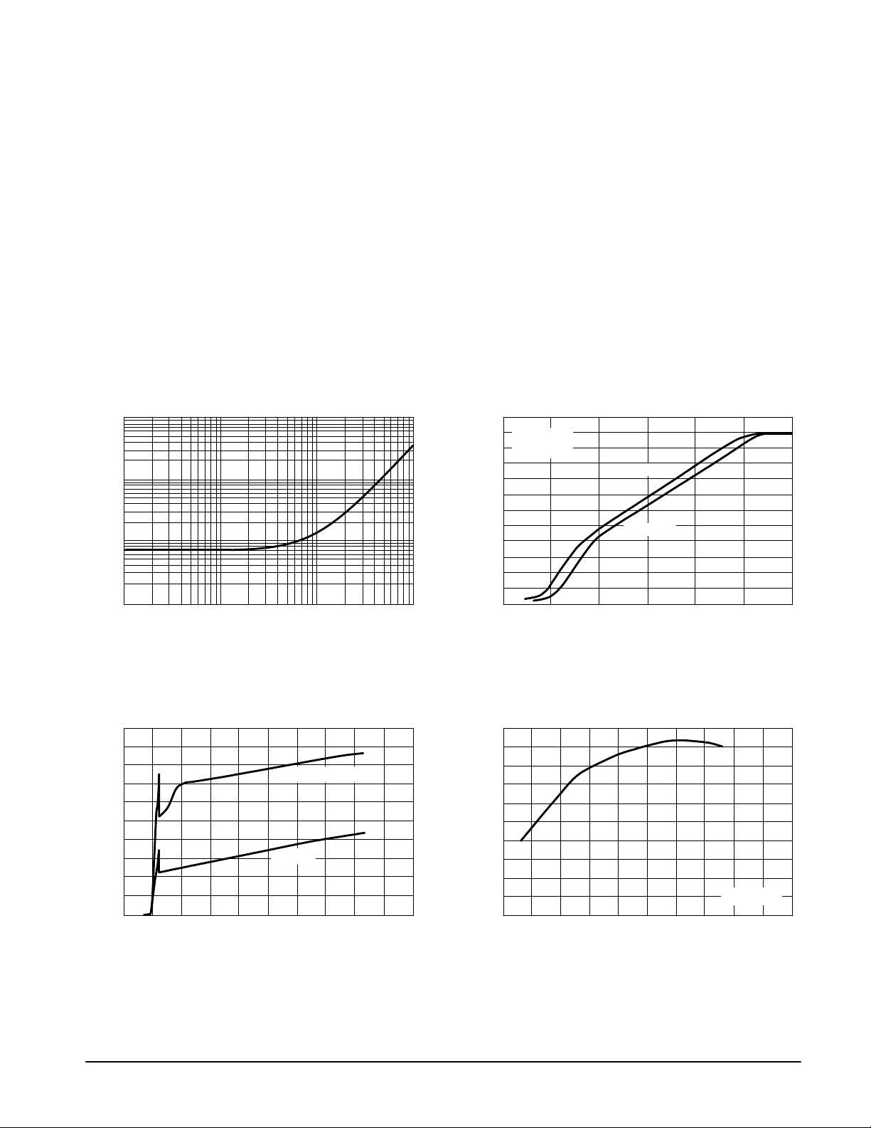
Figure 7. Error Comparator Output Figure 8. Line Transient Response
LP2951C
RL = 330 k
°
C
TA = 25
Figure 6. Dropout V oltage versus Temperature
550
500
L
R
450
400
350
DROPOUT VOLTAGE (mV) = 50
300
8.0
7.5
–50
RL = 50
RL = 50 k
T, TEMPERATURE (°C)
V
in
55
50
45
40
35
30
4.0
2.0
L
R
DROPOUT VOLTAGE (mV) = 50 k
, OUTPUT VOL TAGE (V)
V
SHUTDOWN AND OUTPUT VOLT AGE (V)
out
3.0
2.0
1.0
7.0
6.0
5.0
4.0
3.0
2.0
1.0
–1.0
–100
0
4.70
0
Vin Decreasing
Vin Increasing
4.74 4.78 4.82 4.86 100 200 3004.90 400 500 600 700 800
Vin, INPUT VOLTAGE (V)
7.0
6.5
, INPUT VOLTAGE (V)
in
V
6.0
5.5
0
V
out
TA = 25°C
µ
CL = 1.0
IL = 1.0 mA
F
VO = 5.0 V
t, TIME (µs)
Figure 9. LP2951 Enable Transient Figure 10. Load Transient Response
CL = 1.0 µF
CL = 10 µF
TA = 25°C
IL = 10 mA
Vin = 8.0 V
V
= 5.0 V
Shutdown Input
0 100 200 300 400 40025050 150 200 300 350100
t, TIME (µs)
out
200
150
100
50
LOAD CURRENT (mA)
–50
CL = 1.0 µF
V
out
TA = 25
0
0
= 5.0 V
°
C
I
t, TIME (ms)
Load
V
out
0
– 2.0
– 4.0
OUTPUT VOLTAGE CHANGE (mV)
– 6.0
400
200
0
– 200
OUTPUT VOLTAGE CHANGE (mV)
– 400
6
MOTOROLA ANALOG IC DEVICE DATA

LP2950 LP2951
(
)
Figure 11. Ripple Rejection
80
60
40
TA = 25°C
20
RIPPLE REJECTION (dB)
0
1.0
µ
CL = 1.0
Vin = 6.0 V
V
= 5.0 V
out
F
10 100
Figure 13. Shutdown Threshold Voltage
versus T emperature
1.8
1.6
IL= 0.1 mA
1.0 k
f, FREQUENCY (Hz)
10 k 100 k
4.0
3.0
√
µ
2.0
1.0
VOLTAGE NOISE ( V/ Hz)
0
100
Figure 14. Maximum Rated
100
80
Figure 12. Output Noise
IL= 100 mA
CL = 1.0 µF
CL = 100 µF
1.0 k
f, FREQUENCY (Hz)
TA = 25
VO = 5.0 V
LP2951C
10 k 100 k
Output Current
TA = 25°C
TA = 75°C
°
C
4.0
mV
2.0
SHUTDOWN THRESHOLD VOLTAGE (V)
1.4
1.2
1.0
0.8
–40
– 20 40 80 120 160 5.0 15 25 35 4010 20 3060 100 140200
Output “Off”
Output “On”
t, TEMPERATURE (°C)
, OUTPUT CURRENT (mA)
out
V
60
40
20
LP2951CN
0
0
0
– 2.0
– 4.0
OUTPUT VOLTAGE CHANGE
– 6.0
Vin, INPUT VOLTAGE (V)
MOTOROLA ANALOG IC DEVICE DATA
7

LP2950 LP2951
APPLICATIONS INFORMATION
Introduction
The LP2950/LP2951 regulators are designed with
internal current limiting and thermal shutdown making them
user–friendly. Typical application circuits for the LP2950 and
LP2951 are shown in Figures 17 through 25.
These regulators are not internally compensated and thus
require a 1.0 µF (or greater) capacitance between the
LP2950/LP2951 output terminal and ground for stability.
Most types of aluminum, tantalum or multilayer ceramic will
perform adequately. Solid tantalums or appropriate
multilayer ceramic capacitors are recommended for
operation below 25°C.
At lower values of output current, less output capacitance
is required for output stability. The capacitor can be reduced
to 0.33 µF for currents less than 10 mA, or 0.1 µF for currents
below 1.0 mA. Using the 8–pin versions at voltages less than
5.0 V operates the error amplifier at lower values of gain, so
that more output capacitance is needed for stability. For the
worst case operating condition of a 100 mA load at 1.23 V
output (Output Pin 1 connected to the feedback Pin 7) a
minimum capacitance of 3.3 µF is recommended.
The LP2950 will remain stable and in regulation when
operated with no output load. When setting the output voltage
of the LP2951 with external resistors, the resistance values
should be chosen to draw a minimum of 1.0 µA.
A bypass capacitor is recommended across the
LP2950/LP2951 input to ground if more than 4 inches of
wire connects the input to either a battery or power supply
filter capacitor.
Input capacitance at the LP2951 Feedback Pin 7 can
create a pole, causing instability if high value external
resistors are used to set the output voltage. Adding a 100 pF
capacitor between the Output Pin 1 and the Feedback Pin 7
and increasing the output filter capacitor to at least 3.3 µF will
stabilize the feedback loop.
Error Detection Comparator
The comparator switches to a positive logic low whenever
the LP2951 output voltage falls more than approximately
5.0% out of regulation. This value is the comparator’s
designed–in offset voltage of 60 mV divided by the 1.235 V
internal reference. As shown in the representative block
diagram. This trip level remains 5.0% below normal
regardless of the value of regulated output voltage. For
example, the error flag trip level is 4.75 V for a normal 5.0 V
regulated output, or 9.50 V for a 10 V output voltage.
Figure 1 is a timing diagram which shows the ERROR
signal and the regulated output voltage as the input voltage to
the LP2951 is ramped up and down. The ERROR
becomes valid (low) at about 1.3 V input. It goes high when
the input reaches about 5.0 V (V
exceeds about 4.75 V).
out
Since the LP2951’s dropout voltage is dependent upon the
load current (refer to the curve in the Typical Performance
Characteristics), the input voltage trip point will vary with load
current. The output voltage trip point does not vary with load.
The error comparator output is an open collector which
requires an external pull–up resistor. This resistor may be
returned to the output or some other voltage within the
system. The resistance value should be chosen to be
consistent with the 400 µA sink capability of the error
comparator. A value between 100 k and 1.0 MΩ is suggested.
No pull–up resistance is required if this output is unused.
signal
When operated in the shutdown mode, the error
comparator output will go high if it has been pulled up to an
external supply. To avoid this invalid response, the error
comparator output should be pulled up to V
out
(see
Figure 15).
Figure 15. ERROR Output Timing
5.0 V
Output
Voltage
ERROR
Input
Voltage
Not
Valid
1.3 V
4.75 V
4.75 V + V
dropout
4.70 V
4.70 V + V
1.3 V
Not
Valid
dropout
Pull–Up
to Ext
Pull–Up
to V
out
Programming the Output Voltage (LP2951)
The LP2951CX may be pin–strapped for 5.0 V using its
internal voltage divider by tying Pin 1 (output) to Pin 2 (sense)
and Pin 7 (feedback) to Pin 6 (5.0 V tap). Alternatively , it may
be programmed for any output voltage between its 1.235
reference voltage and its 30 V maximum rating. An external
pair of resistors is required, as shown in Figure 16.
Figure 16. Adjustable Regulator
V
in
Error
Output
Shutdown
Input
100 k
5
3
8
V
in
Error
SD
V
SNS
V
O
Gnd FB
47
out
T
1
2
NC
6
NC
R1
R
0.01
2
µ
F
V
out
1.23 to 30 V
3.3
µ
F
The complete equation for the output voltage is:
(
V
1)R1ńR2))
ref
IFBR1
FB
where V
V
+
out
is the nominal 1.235 V reference voltage and I
ref
is the feedback pin bias current, nominally –20 nA. The
minimum recommended load current of 1.0 µA forces an
upper limit of 1.2 MΩ on the value of R2, if the regulator must
work with no load. IFB will produce a 2% typical error in V
out
which may be eliminated at room temperature by adjusting
R1. For better accuracy, choosing R2 = 100 k reduces this
8
MOTOROLA ANALOG IC DEVICE DATA

LP2950 LP2951
error to 0.17% while increasing the resistor program current
to 12 µA. Since the LP2951 typically draws 75 µA at no load
with Pin 2 open circuited, the extra 12 µA of current drawn is
often a worthwhile tradeoff for eliminating the need to set
output voltage in test.
Output Noise
In many applications it is desirable to reduce the noise
present at the output. Reducing the regulator bandwidth by
increasing the size of the output capacitor is the only method
for reducing noise on the 3 lead LP2950. However,
increasing the capacitor from 1.0 µF to 220 µF only
decreases the noise from 430 µV to 160 µVrms for a 100 kHz
bandwidth at the 5.0 V output.
Noise can be reduced fourfold by a bypass capacitor
across R1, since it reduces the high frequency gain from 4 to
unity. Pick
C
Bypass
[
or about 0.01 µF. When doing this, the output capacitor
must be increased to 3.3 µF to maintain stability. These
changes reduce the output noise from 430 µV to 126 µVrms
for a 100 kHz bandwidth at 5.0 V output. With bypass
capacitor added, noise no longer scales with output voltage
so that improvements are more dramatic at higher output
voltages.
1
2pR1 x 200 Hz
Figure 17. 1.0 A Regulator with 1.2 V Dropout
Unregulated
Input
1.0 µF
Error
Output
Shutdown
Input
10 k
V
5
Error
LP2951CN
3
SD
Gnd FB
47
8
in
V
out
SNS
V
O
1
2
6
T
1.0 M
0.01 µF
0.002 µF
MTB23P06E
2.0 k
V
out
5.0 V
0 to 1.0 A
µ
220
±
1.0%
F
MOTOROLA ANALOG IC DEVICE DATA
9

LP2950 LP2951
TYPICAL APPLICATIONS
Figure 18. Lithium Ion Battery Cell Charger
Unregulated Input
6.0 to 10 Vdc
8
Gnd
NC
0.1 µF
V
5
Error
LP2951CN
3
SD
Gnd FB
47
in
V
out
SNS
V
T
O
1
2
6
NC
NC
1N4001
330 pF
2.2 µF
Figure 20. Latch Off When Error Flag Occurs
4.2 V ±0.025 V
2.0 M
1.0%
806 k
1.0%
50 k
Lithium Ion
Rechargeable
Cell
Figure 19. Low Drift Current Sink
+V = 2.0 to 30 V
I
Error
Output
Shutdown
Input
L
5
Error
3
SD
LP2951CN
Gnd FB
Load
V
47
8
in
V
out
SNS
V
T
O
IL = 1.23/R
1
2
6
R
1.0
0.1 µF
µ
F
Figure 21. 5.0 V Regulator with 2.5 V Sleep Function
470 k
5
2N3906
Reset
Normally
Closed
Error flag occurs when Vin is too low to
maintain V
excessive load current.
470 k
out
Error
3
SD
, or if V
LP2951CN
+V
in
8
V
in
V
out
SNS
V
T
O
Gnd FB
47
is reduced by
out
1
2
NC
6
NC
R1
R2
1.0
+V
in
*Sleep
Input
V
out
µ
F
47 k
Error
Output
Shutdown
Input
5
Error
LP2951CN
3
SD
Gnd FB
47
8
V
in
V
CMOS
Gate
1
V
out
2
SNS
6
T
O
NC
NC
470 k
2N3906
200 k
100 k
100 k
100 pF
V
3.3
out
µ
F
10
MOTOROLA ANALOG IC DEVICE DATA

LP2950 LP2951
Figure 22. Regulator with Early Warning and Auxiliary Output
+V
in
8
NC
V
5
Error
LP2951CN
#1
3
SD
Gnd FB
47
in
V
out
SNS
V
O
1
2
6
T
D1
1.0
D2
µ
Memory
V+
F
20
3.6 V
NiCad
Q1
2N3906
2.7 M
D4
330 k
Error
Flag
5
3
2N3906
4.7 M
20 k
27 k
D3
Early Warning
Reset
µ
P
V
DD
8
V
in
1
#2
V
out
2
SNS
6
V
T
O
Main
Output
1.0 µF
Error
LP2951CN
SD
Gnd FB
47
Figure 23. 2.0 A Low Dropout Regulator
+V
.33 µF
NC
NC
in
0.05
MJE2955
47
4.7 µF
R1
Current Limit
Section
680
2N3906
5
220
3
10 k
8
V
in
Error
SD
V
SNS
LP2951CN
V
out
O
Gnd FB
47
470
T
1
2
6
.01 µF
All diodes are 1N4148.
Early Warning flag on low input voltage.
Main output latches off at lower input
voltages.
Battery backup on auxiliary output.
Operation: Regulator #1’s V
programmed one diode drop above 5.0 V.
Its error flag becomes active when Vin <
V. When Vin drops below 5.3 V, the error
flag of regulator #2 becomes active and via
Q1 latches the main output “off”. When V
again exceeds 5.7 V, regulator #1 is back in
regulation and the early warning signal
rises, unlatching regulator #2 via D3.
out
is
1000 µF
V
@ 2.0 A
out
Tant
100 µF
5.7
in
0.033 µF
V
= 1.25V (1.0 + R1/R2)
out
For 5.0 V output, use internal resistors. Wire Pin 6 to 7,
and wire Pin 2 to +V
MOTOROLA ANALOG IC DEVICE DATA
out
R2
Bus.
11

1N4001
ÎÎÎ
ÎÎÎ
ÎÎÎ
LP2950 LP2951
Figure 24. Open Circuit Detector for
4.0 to 20 mA Current Loop
+5.0 V
4.7 k
20 mA4
NC
NC
0.1 µF
V
5
Error
LP2951CN
3
SD
Gnd FB
47
8
in
V
out
SNS
V
O
15
24
1
2
NC
6
T
NC
1N457
1N457
1N457
* High for
IL < 3.5 mA
360
Output*
2
MC34164P–5
3
Figure 25. Low Battery Disconnect
100 k
1
31.6 k
2N3906
NC
V
5
Error
LP2951CN
3
SD
Gnd FB
47
8
in
V
out
SNS
V
O
NC
T
1
2
6
Figure 26. DP AK Thermal Resistance and Maximum
Power Dissipation versus P.C.B. Copper Length
°
100
90
80
70
Free Air
Mounted
Vertically
Minimum
Size Pad
P
D(max)
for TA = 50°C
2.0 oz. Copper
L
6.0 V Lead–Acid
Battery
1.0 µF
NC
L
Main V+
Memory V+
20
NiCad Backup
Battery
2.4
2.0
1.6
1.2
12
60
JA
JUNCTION-TO-AIR ( C/W)
θ
R , THERMAL RESISTANCE
50
40
010203025155.0
R
θ
JA
L, LENGTH OF COPPER (mm)
0.8
0.4
, MAXIMUM POWER DISSIPATION (W)
D
P
0
MOTOROLA ANALOG IC DEVICE DATA

SEATING
PLANE
LP2950 LP2951
OUTLINE DIMENSIONS
Z SUFFIX
PLASTIC PACKAGE
CASE 29–04
(TO–226AA/TO–92)
ISSUE AD
A
B
R
P
L
XX
H
V
1
F
G
K
D
J
C
SECTION X–X
N
N
NOTES:
1. DIMENSIONING AND TOLERANCING PER ANSI
Y14.5M, 1982.
2. CONTROLLING DIMENSION: INCH.
3. CONTOUR OF PACKAGE BEYOND DIMENSION R
IS UNCONTROLLED.
4. DIMENSION F APPLIES BETWEEN P AND L.
DIMENSION D AND J APPLY BETWEEN L AND K
MINIMUM. LEAD DIMENSION IS UNCONTROLLED
IN P AND BEYOND DIMENSION K MINIMUM.
DIM MIN MAX MIN MAX
A 0.175 0.205 4.45 5.20
B 0.170 0.210 4.32 5.33
C 0.125 0.165 3.18 4.19
D 0.016 0.022 0.41 0.55
F 0.016 0.019 0.41 0.48
G 0.045 0.055 1.15 1.39
H 0.095 0.105 2.42 2.66
J 0.015 0.020 0.39 0.50
K 0.500 ––– 12.70 –––
L 0.250 ––– 6.35 –––
N 0.080 0.105 2.04 2.66
P ––– 0.100 ––– 2.54
R 0.115 ––– 2.93 –––
V 0.135 ––– 3.43 –––
MILLIMETERSINCHES
DT SUFFIX
PLASTIC PACKAGE
CASE 369A–13
(DPAK)
ISSUE Y
NOTES:
SEATING
–T–
PLANE
B
V
S
R
4
A
123
K
F
L
D
2 PL
G
0.13 (0.005) T
C
E
Z
U
J
H
M
1. DIMENSIONING AND TOLERANCING PER ANSI
Y14.5M, 1982.
2. CONTROLLING DIMENSION: INCH.
DIM MIN MAX MIN MAX
A 0.235 0.250 5.97 6.35
B 0.250 0.265 6.35 6.73
C 0.086 0.094 2.19 2.38
D 0.027 0.035 0.69 0.88
E 0.033 0.040 0.84 1.01
F 0.037 0.047 0.94 1.19
G 0.180 BSC 4.58 BSC
H 0.034 0.040 0.87 1.01
J 0.018 0.023 0.46 0.58
K 0.102 0.114 2.60 2.89
L 0.090 BSC 2.29 BSC
R 0.175 0.215 4.45 5.46
S 0.020 0.050 0.51 1.27
U 0.020 ––– 0.51 –––
V 0.030 0.050 0.77 1.27
Z 0.138 ––– 3.51 –––
MILLIMETERSINCHES
MOTOROLA ANALOG IC DEVICE DATA
13

NOTE 2
–T–
SEATING
PLANE
LP2950 LP2951
OUTLINE DIMENSIONS
N SUFFIX
PLASTIC PACKAGE
CASE 626–05
ISSUE K
NOTES:
1. DIMENSION L TO CENTER OF LEAD WHEN
58
–B–
1
4
F
–A–
L
C
J
N
D
H
G
0.13 (0.005)
K
M M M
AB
T
M
FORMED PARALLEL.
2. PACKAGE CONTOUR OPTIONAL (ROUND OR
SQUARE CORNERS).
3. DIMENSIONING AND TOLERANCING PER ANSI
Y14.5M, 1982.
MILLIMETERS INCHES
MIN MINMAX MAX
DIM
A
B
C
D
F
G
H
J
K
L
M
N
9.40
6.10
3.94
0.38
1.02
2.54 BSC
0.76
0.20
2.92
7.62 BSC
–
0.76
10.16
6.60
4.45
0.51
1.78
1.27
0.30
3.43
10
1.01
°
0.370
0.240
0.155
0.015
0.040
0.100 BSC
0.030
0.008
0.115
0.300 BSC
–
0.030
0.400
0.260
0.175
0.020
0.070
0.050
0.012
0.135
10
0.040
°
A
C
A1
D SUFFIX
PLASTIC PACKAGE
CASE 751–05
(SO–8)
ISSUE R
D
58
0.25MB
E
1
B
e
H
4
M
h
X 45
_
q
C
A
SEATING
PLANE
0.10
L
B
SS
A0.25MCB
NOTES:
1. DIMENSIONING AND TOLERANCING PER ASME
Y14.5M, 1994.
2. DIMENSIONS ARE IN MILLIMETERS.
3. DIMENSION D AND E DO NOT INCLUDE MOLD
PROTRUSION.
4. MAXIMUM MOLD PROTRUSION 0.15 PER SIDE.
5. DIMENSION B DOES NOT INCLUDE MOLD
PROTRUSION. ALLOWABLE DAMBAR
PROTRUSION SHALL BE 0.127 TOTAL IN EXCESS
OF THE B DIMENSION AT MAXIMUM MATERIAL
CONDITION.
MILLIMETERS
DIM MIN MAX
A 1.35 1.75
A1 0.10 0.25
B 0.35 0.49
C 0.18 0.25
D 4.80 5.00
E
3.80 4.00
1.27 BSCe
H 5.80 6.20
h
0.25 0.50
L 0.40 1.25
0 7
q
__
14
MOTOROLA ANALOG IC DEVICE DATA

PIN 1 ID
SEATING
PLANE
–T–
0.038 (0.0015)
LP2950 LP2951
OUTLINE DIMENSIONS
DM SUFFIX
PLASTIC PACKAGE
CASE 846A–02
(Micro–8)
ISSUE C
NOTES:
–A–
K
G
–B–
8 PL
D
0.08 (0.003) A
M
T
S
B
S
C
1. DIMENSIONING AND TOLERANCING PER ANSI
Y14.5M, 1982.
2. CONTROLLING DIMENSION: MILLIMETER.
3. DIMENSION A DOES NOT INCLUDE MOLD FLASH,
PROTRUSIONS OR GATE BURRS. MOLD FLASH,
PROTRUSIONS OR GATE BURRS SHALL NOT
EXCEED 0.15 (0.006) PER SIDE.
4. DIMENSION B DOES NOT INCLUDE INTERLEAD
FLASH OR PROTRUSION. INTERLEAD FLASH OR
PROTRUSION SHALL NOT EXCEED 0.25 (0.010)
PER SIDE.
DIM MIN MAX MIN MAX
A 2.90 3.10 0.114 0.122
B 2.90 3.10 0.114 0.122
C ––– 1.10 ––– 0.043
D 0.25 0.40 0.010 0.016
G 0.65 BSC 0.026 BSC
H 0.05 0.15 0.002 0.006
J 0.13 0.23 0.005 0.009
K 4.75 5.05 0.187 0.199
L 0.40 0.70 0.016 0.028
INCHESMILLIMETERS
H
J
L
MOTOROLA ANALOG IC DEVICE DATA
15

LP2950 LP2951
Motorola reserves the right to make changes without further notice to any products herein. Motorola makes no warranty , representation or guarantee regarding
the suitability of its products for any particular purpose, nor does Motorola assume any liability arising out of the application or use of any product or circuit, and
specifically disclaims any and all liability, including without limitation consequential or incidental damages. “T ypical” parameters which may be provided in Motorola
data sheets and/or specifications can and do vary in different applications and actual performance may vary over time. All operating parameters, including “Typicals”
must be validated for each customer application by customer’s technical experts. Motorola does not convey any license under its patent rights nor the rights of
others. Motorola products are not designed, intended, or authorized for use as components in systems intended for surgical implant into the body, or other
applications intended to support or sustain life, or for any other application in which the failure of the Motorola product could create a situation where personal injury
or death may occur. Should Buyer purchase or use Motorola products for any such unintended or unauthorized application, Buyer shall indemnify and hold Motorola
and its officers, employees, subsidiaries, affiliates, and distributors harmless against all claims, costs, damages, and expenses, and reasonable attorney fees
arising out of, directly or indirectly, any claim of personal injury or death associated with such unintended or unauthorized use, even if such claim alleges that
Motorola was negligent regarding the design or manufacture of the part. Motorola and are registered trademarks of Motorola, Inc. Motorola, Inc. is an Equal
Opportunity/Affirmative Action Employer.
How to reach us:
USA/EUROPE/Locations Not Listed: Motorola Literature Distribution; JAPAN: Nippon Motorola Ltd.; Tatsumi–SPD–JLDC, 6F Seibu–Butsuryu–Center,
P.O. Box 20912; Phoenix, Arizona 85036. 1–800–441–2447 or 602–303–5454 3–14–2 T atsumi Koto–Ku, Tokyo 135, Japan. 03–81–3521–8315
MFAX: RMF AX0@email.sps.mot.com – TOUCHT ONE 602–244–6609 ASIA/PACIFIC: Motorola Semiconductors H.K. Ltd.; 8B Tai Ping Industrial Park,
INTERNET: http://Design–NET.com 51 Ting Kok Road, Tai Po, N.T., Hong Kong. 852–26629298
16
◊
MOTOROLA ANALOG IC DEVICE DATA
LP2950/D
*LP2950/D*
 Loading...