

Page 1
查询LM2931/D供应商
Order this document by LM2931/D
The LM2931 series consists of positive fixed and adjustable output
voltage regulators that are specifically designed to maintain proper
regulation with an extremely low input–to–output voltage differential. These
devices are capable of supplying output currents in excess of 100 mA and
feature a low bias current of 0.4 mA at 10 mA output.
Designed primarily to survive in the harsh automotive environment, these
devices will protect all external load circuitry from input fault conditions
caused by reverse battery connection, two battery jump starts, and
excessive line transients during load dump. This series also includes internal
current limiting, thermal shutdown, and additionally, is able to withstand
temporary power–up with mirror–image insertion.
Due to the low dropout voltage and bias current specifications, the
LM2931 series is ideally suited for battery powered industrial and consumer
equipment where an extension of useful battery life is desirable. The ‘C’
suffix adjustable output regulators feature an output inhibit pin which is
extremely useful in microprocessor–based systems.
• Input–to–Output Voltage Differential of < 0.6 V @ 100 mA
• Output Current in Excess of 100 mA
• Low Bias Current
• 60 V Load Dump Protection
• –50 V Reverse Transient Protection
• Internal Current Limiting with Thermal Shutdown
• Temporary Mirror–Image Protection
• Ideally Suited for Battery Powered Equipment
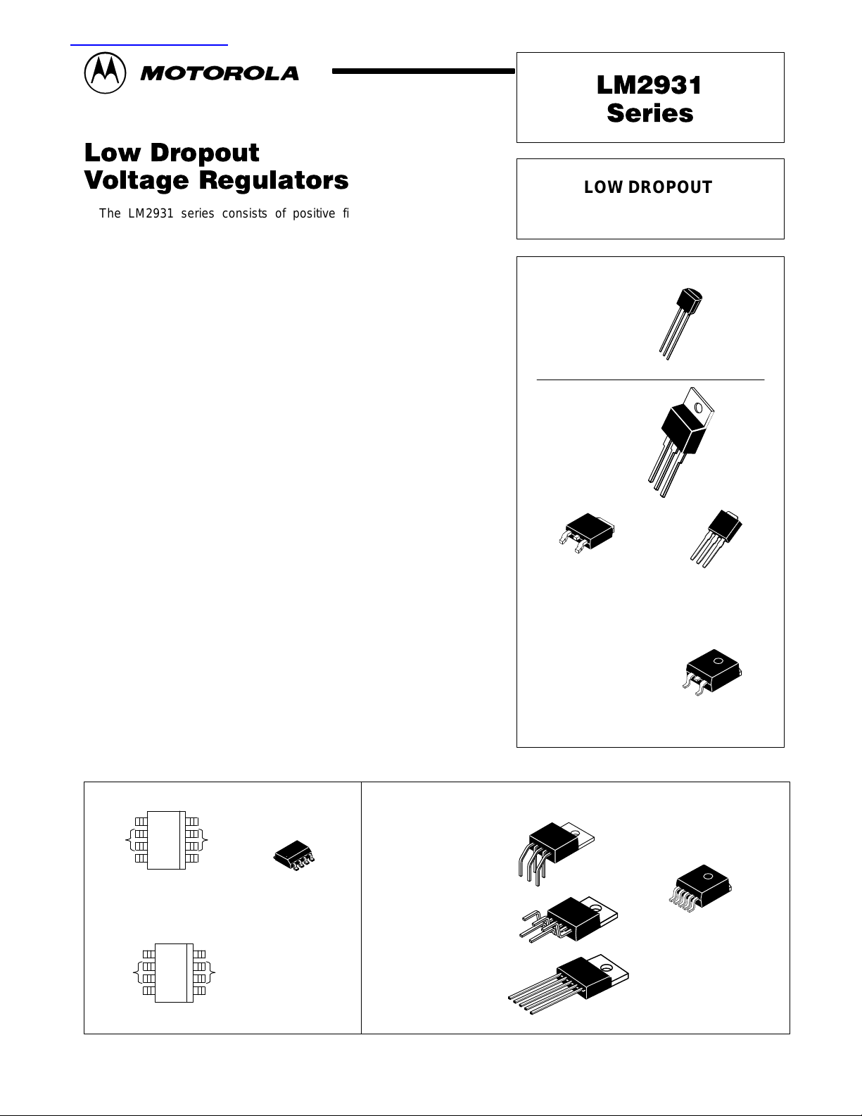
• Economical 5–Lead TO–220 Package with T wo Optional Leadforms
• Available in Surface Mount SOP–8, D
• High Accuracy (±2%) Reference (LM2931AC) Available
(See Following Page for Ordering Information.)
2
P AK and DPAK Packages
LOW DROPOUT
VOLTAGE REGULATORS
FIXED OUTPUT VOLTAGE
Z SUFFIX
PLASTIC PACKAGE
CASE 29
1
2
3
T SUFFIX
PLASTIC PACKAGE
CASE 221A
Heatsink surface
connected to Pin 2.
1
3
DT SUFFIX
PLASTIC PACKAGE
CASE 369A
(DPAK)
D2T SUFFIX
PLASTIC PACKAGE
CASE 936
(D2PAK)
Heatsink surface (shown as terminal 4 in
case outline drawing) is connected to Pin 2.
1
2
3
1
2
DT–1 SUFFIX
PLASTIC PACKAGE
CASE 369
(DPAK)
2
1
3
Pin 1. Output
2. Ground
3. Input
Pin 1. Input
2. Ground
3. Output
3
FIXED
N.C.
Gnd
Input
Output
Inhibit
Gnd
Input
54
(Top View)
ADJUSTABLE
54
(Top View)
N.C.
Gnd
Output18
Adjust
Gnd
Output18
8
D SUFFIX
PLASTIC PACKAGE
CASE 751
(SOP–8)
1
MOTOROLA ANALOG IC DEVICE DATA
ADJUSTABLE OUTPUT VOLTAGE
TH SUFFIX
PLASTIC PACKAGE
CASE 314A
1
5
TV SUFFIX
PLASTIC PACKAGE
CASE 314B
T SUFFIX
PLASTC PACKAGE
CASE 314D
Heatsink surface connected to Pin 3.
1
1
5
Motorola, Inc. 1997 Rev 4
Pin 1. Adjust
2. Output Inhibit
3. Ground
4. Input
5. Output
1
5
5
D2T SUFFIX
PLASTIC PACKAGE
CASE 936A
(D2PAK)
Heatsink surface (shown as
terminal 6 in case outline
drawing) is connected to Pin 3.
1
Page 2
LM2931 Series
±3.8%
5.0 V
j
ORDERING INFORMATION
Output
Device
LM2931AD–5.0
LM2931ADT–5.0
LM2931ADT–1–5.0
LM2931AD2T–5.0
LM2931A T–5.0
LM2931AZ–5.0
LM2931D–5.0
LM2931D2T–5.0
LM2931DT–5.0
LM2931DT–1–5.0
LM2931T–5.0
LM2931Z–5.0
LM2931CD
LM2931CD2T
LM2931CT
LM2931CTH
LM2931CTV 314B 5–Pin Vertical Leadform
LM2931ACD
LM2931ACD2T
LM2931ACT
LM2931ACTH 314A 5–Pin Horizontal Leadform
LM2931ACTV 314B 5–Pin Vertical Leadform
Voltage Tolerance
±5.0%
Adjustable
Adjustable ±2.0%
Case Package
751 SOP–8 Surface Mount
369A Surface Mount DPAK
369 DPAK
936 Surface Mount D2PAK
221A TO–220 Type
29 TO–92 Type
751 SOP–8 Surface Mount
936 Surface Mount D2PAK
369A Surface Mount DPAK
369 DPAK
221A TO–220 Type
29 TO–92 Type
751 SOP–8 Surface Mount
936A Surface Mount D2PAK
314D 5–Pin TO–220 Type
314A 5–Pin Horizontal Leadform
751 SOP–8 Surface Mount
936A Surface Mount D2PAK
314D 5–Pin TO–220 Type
Input
Output
30 k *
Adjust
92.8 k *
Ground
*Deleted on Adjustable Regulators
6.0
30 k
3.94 k
3.0 k
11.5 k
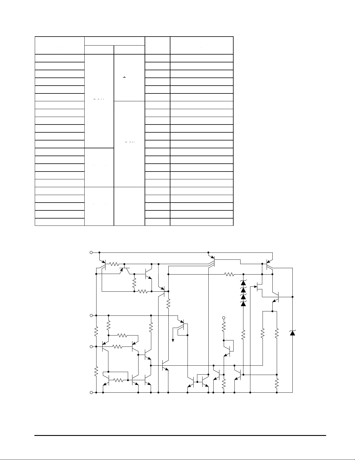
Representative Schematic Diagram
6.0 k
350
500
30 k
EPI
Bias
This device contains 26 active transistors.
50 k
30 k
Output
Inhibit
35 k
6.8 V
48 k
180 k 184 k
10 k
5.8 V
2
MOTOROLA ANALOG IC DEVICE DATA
Page 3
LM2931 Series
MAXIMUM RATINGS
Rating Symbol Value Unit
Input Voltage Continuous V
I
Transient Input V oltage (τ ≤100 ms) VI(τ) 60 Vpk
Transient Reverse Polarity Input V oltage –VI(τ) –50– Vpk
1.0% Duty Cycle, τ ≤ 100 ms
Power Dissipation
Case 29 (TO–92 Type)
TA = 25°C P
Thermal Resistance, Junction–to–Ambient R
Thermal Resistance, Junction–to–Case R
D
θJA
θJC
Case 221A, 314A, 314B and 314D (TO–220 T ype)
TA = 25°C P
Thermal Resistance, Junction–to–Ambient R
Thermal Resistance, Junction–to–Case R
D
θJA
θJC
Case 369 and 369A (DPAK) [Note 1]
TA = 25°C P
Thermal Resistance, Junction–to–Ambient R
Thermal Resistance, Junction–to–Case R
D
θJA
θJC
Case 751 (SOP–8) [Note 2]
TA = 25°C P
Thermal Resistance, Junction–to–Ambient R
Thermal Resistance, Junction–to–Case R
D
θJA
θJC
Case 936 and 936A (D2PAK) [Note 3]
TA = 25°C P
Thermal Resistance, Junction–to–Ambient R
Thermal Resistance, Junction–to–Case R
Tested Operating Junction Temperature Range T
Storage Temperature Range T
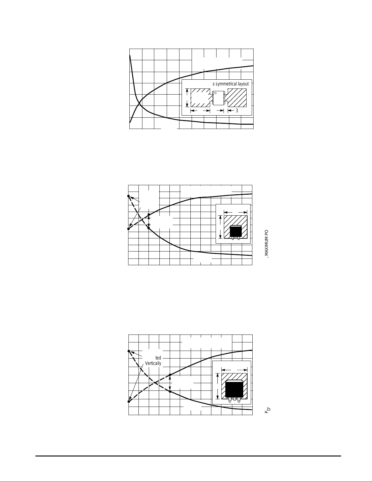
NOTES: 1. DPAK Junction–to–Ambient Thermal Resistance is for vertical mounting. Refer to Figure 24 for
board mounted Thermal Resistance.
2.SOP–8 Junction–to–Ambient Thermal Resistance is for minimum recommended pad size. Refer
to Figure 23 for Thermal Resistance variation versus pad size.
3.D2PAK Junction–to–Ambient Thermal Resistance is for vertical mounting. Refer to Figure 25 for
board mounted Thermal Resistance.
4.ESD data available upon request.
D
θJA
θJC
J
stg
40 Vdc
Internally Limited W
178 °C/W
83 °C/W
Internally Limited W
65 °C/W
5.0 °C/W
Internally Limited W
92 °C/W
6.0 °C/W
Internally Limited W
160 °C/W
25 °C/W
Internally Limited W
70 °C/W
5.0 °C/W
–40 to +125 °C
–65 to +150 °C
ELECTRICAL CHARACTERISTICS (V
= 14 V, IO = 10 mA, CO = 100 µF, C
in
= 0.3 Ω, TJ = 25°C [Note 1].)
O(ESR)
LM2931–5.0 LM2931A–5.0
Characteristic Symbol
Min Typ Max Min Typ Max
Unit
FIXED OUTPUT
Output Voltage V
O
V
Vin = 14 V, IO = 10 mA, TJ = 25°C 4.75 5.0 5.25 4.81 5.0 5.19
Vin = 6.0 V to 26 V, IO ≤ 100 mA, TJ = –40° to +125°C 4.50 – 5.50 4.75 – 5.25
Line Regulation Reg
line
mV
Vin = 9.0 V to 16 V – 2.0 10 – 2.0 10
Vin = 6.0 V to 26 V – 4.0 30 – 4.0 30
Load Regulation (IO = 5.0 mA to 100 mA) Reg
Output Impedance Z
load
O
– 14 50 – 14 50 mV
mΩ
IO = 10 mA, ∆IO = 1.0 mA, f = 100 Hz to 10 kHz – 200 – – 200 –
Bias Current I
B
mA
Vin = 14 V, IO = 100 mA, TJ = 25°C – 5.8 30 – 5.8 30
Vin = 6.0 V to 26 V, IO = 10 mA, TJ = –40° to +125°C – 0.4 1.0 – 0.4 1.0
Output Noise Voltage (f = 10 Hz to 100 kHz) V
n
– 700 – – 700 – µVrms
Long Term Stability S – 20 – – 20 – mV/kHR
NOTES: 1. Low duty cycle pulse techniques are used during test to maintain junction temperature as close to ambient as possible.
2.The reference voltage on the adjustable device is measured from the output to the adjust pin across R1.
MOTOROLA ANALOG IC DEVICE DATA
3
Page 4
LM2931 Series
ELECTRICAL CHARACTERISTICS
Characteristic Symbol
FIXED OUTPUT
Ripple Rejection (f = 120 Hz) RR 60 90 – 60 90 – dB
Dropout Voltage VI–V
IO = 10 mA – 0.015 0.2 – 0.015 0.2
IO = 100 mA – 0.16 0.6 – 0.16 0.6
Over–Voltage Shutdown Threshold V
Output Voltage with Reverse Polarity Input (Vin = –15 V) –V
ELECTRICAL CHARACTERISTICS (V
Characteristic Symbol Min Typ Max Min Typ Typ Unit
ADJUSTABLE OUTPUT
Reference Voltage (Note 2, Figure 18) V
IO = 10 mA, TJ = 25°C 1.14 1.20 1.26 1.17 1.20 1.23
IO ≤ 100 mA, TJ = –40 to +125°C 1.08 – 1.32 1.15 – 1.25
Output Voltage Range VO
Line Regulation (Vin = VO + 0.6 V to 26 V) Reg
Load Regulation (IO = 5.0 mA to 100 mA) Reg
Output Impedance Z
IO = 10 mA, ∆IO = 1.0 mA, f = 10 Hz to 10 kHz – 40 – – 40 –
Bias Current I
IO = 100 mA – 6.0 – – 6.0 –
IO = 10 mA – 0.4 1.0 – 0.4 1.0
Output Inhibited (V
Adjustment Pin Current I
Output Noise Voltage (f = 10 Hz to 100 kHz) V
Long–Term Stability S – 0.4 – – 0.4 – %/kHR
Ripple Rejection (f = 120 Hz) RR 0.10 0.003 – 0.10 0.003 – %/V
Dropout Voltage VI–V
IO = 10 mA – 0.015 0.2 – 0.015 0.2
IO = 100 mA – 0.16 0.6 – 0.16 0.6
Over–Voltage Shutdown Threshold V
Output Voltage with Reverse Polarity Input (Vin = –15 V) –V
Output Inhibit Threshold Voltages V
Output “On”: TJ = 25°C – 2.15 1.90 – 2.15 1.90
Output “Off”: TJ = 25°C 2.50 2.26 – 2.50 2.26 –
Output Inhibit Threshold Current (V
NOTES: 1. Low duty cycle pulse techniques are used during test to maintain junction temperature as close to ambient as possible.
2.The reference voltage on the adjustable device is measured from the output to the adjust pin across R1.
= 2.5 V) – 0.2 1.0 – 0.2 1.0
th(OI)
TJ = –40° to +125°C – – 1.20 – – 1.20
TJ = –40° to +125°C 3.25 – – 3.25 – –
(Vin = 14 V, IO = 10 mA, CO = 100 µF, C
th(OV)
O
= 14 V, IO = 10 mA, CO = 100 µF, C
in
ref
range
line
load
O
B
Adj
n
th(OV)
O
th(OI)
= 2.5 V) I
th(OI)
th(OI)
= 0.3 Ω, TJ = 25°C [Note 1].)
O(ESR)
LM2931–5.0 LM2931A–5.0
Min Typ Max Min Typ Max
O
26 29.5 40 26 29.5 40 V
–0.3 0 – –0.3 0 – V
= 0.3 Ω, TJ = 25°C [Note 1].)
O(ESR)
LM2931C LM2931AC
3.0 to242.7 to
29.5
– 0.2 1.5 – 0.2 1.5 mV/V
– 0.3 1.0 – 0.3 1.0 %/V
– 0.2 – – 0.2 – µA
– 140 – – 140 – µVrms/V
O
26 29.5 40 26 29.5 40 V
–0.3 0 – –0.3 0 – V
– 30 50 – 30 50 µA
– 3.0 to242.7 to
29.5
Unit
– V
mΩ/V
mA
V
V
V
V
4
MOTOROLA ANALOG IC DEVICE DATA
Page 5
LM2931 Series
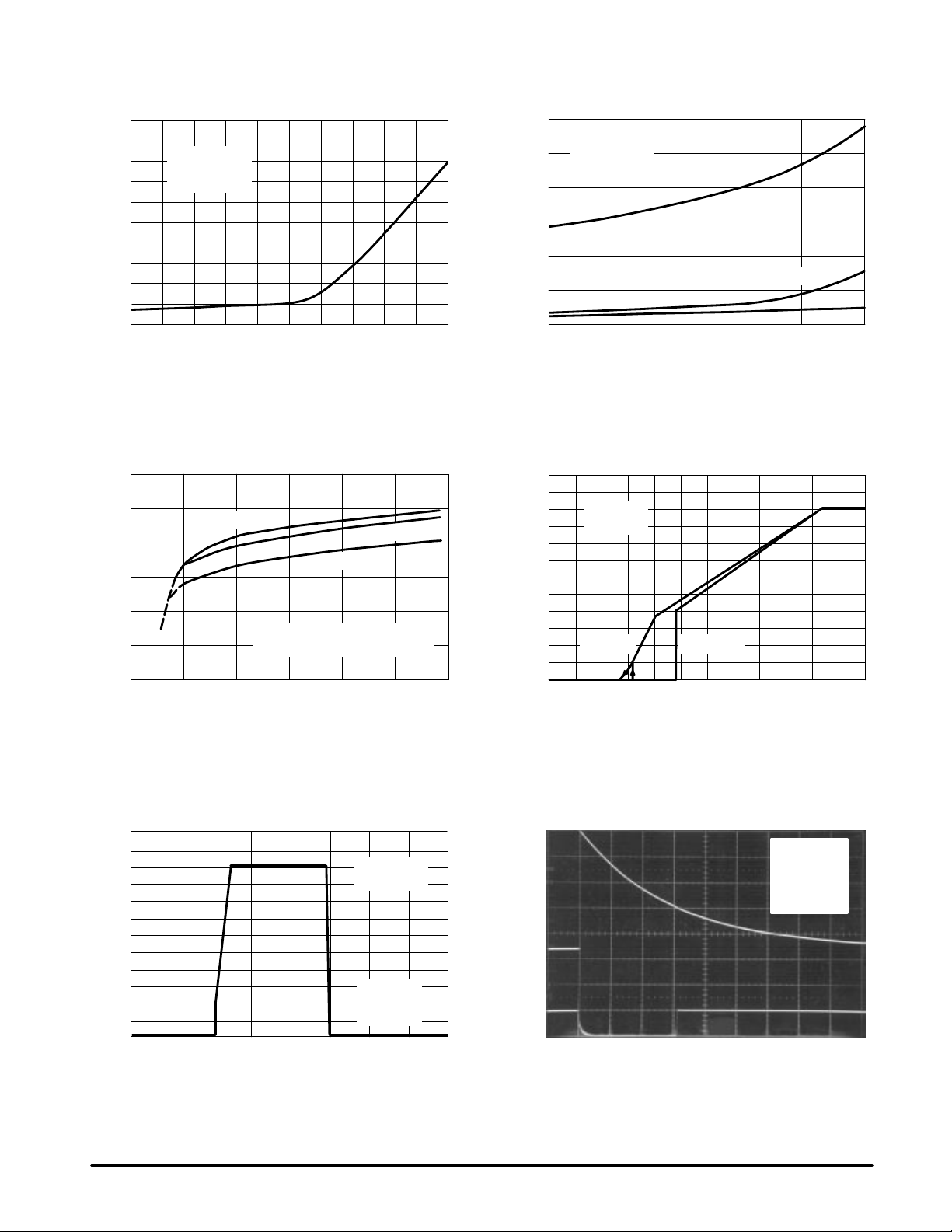
Figure 1. Dropout Voltage versus Output Current
200
Vin = 14 V
∆
V
= 100 mV
out
°
C
TJ = 25
0 20 40 60 80 100
IO, OUTPUT CURRENT (mA)
, DROPOUT VOLTAGE (mV)V
–V
160
120
80
40
in O
0
300
Vin = 14 V
∆
V
200
100
, DROPOUT VOLTAGE (mV)V
–V
in O
0
0 25 50 75 100 125
Junction T emperature
= 100 mV
out
TJ, JUNCTION TEMPERATURE (°C)
IO = 100 mA
IO = 50 mA
IO = 10 mA
Figure 3. Peak Output Current versus Input Voltage Figure 4. Output Voltage versus Input Voltage
Figure 2. Dropout Voltage versus
350
250
TJ = –40°C
TJ = 25°C
TJ = 85°C
6.0
5.0
4.0
3.0
V
= 5.0 V
out
TA = 25
°
C
150
, OUTPUT CURRENT (mA)
O
I
50
0 5.0 10 15 20 25 30
Dashed lines below Vin = 5.0 V
are for Adjustable output devices only.
Vin, INPUT VOLTAGE (V)
2.0
, OUTPUT VOL TAGE (V)
O
V
1.0
0
RL = 50
Ω
0 1.0 2.0 3.0 4.0 5.0 6.0
IO = 100 mA
Vin, INPUT VOLTAGE (V)
Figure 5. Output V oltage versus Input Voltage Figure 6. Load Dump Characteristics
6.0
5.0
4.0
3.0
2.0
, OUTPUT VOL TAGE (V)
O
V
1.0
0
–20 –10 0 10 20 30 40 50 60
Vin, INPUT VOLTAGE (V)
VCC = 15 V
V
= 5.05 V
FB1
V
= 5.0 V
out
Ω
RL = 500
TA = 25°C
(10 V/DIV)
, INPUT VOLTAGE, OUTPUT VOL TAGE
in
V
0
0
(5.0 V/DIV)
O
V
t, TIME (50 ms/DIV)
V
= 5.0 V
out
Ω
RL = 50
CO = 100 µF
τ
= 150 ms
°
C
TA = 25
MOTOROLA ANALOG IC DEVICE DATA
5
Page 6
LM2931 Series
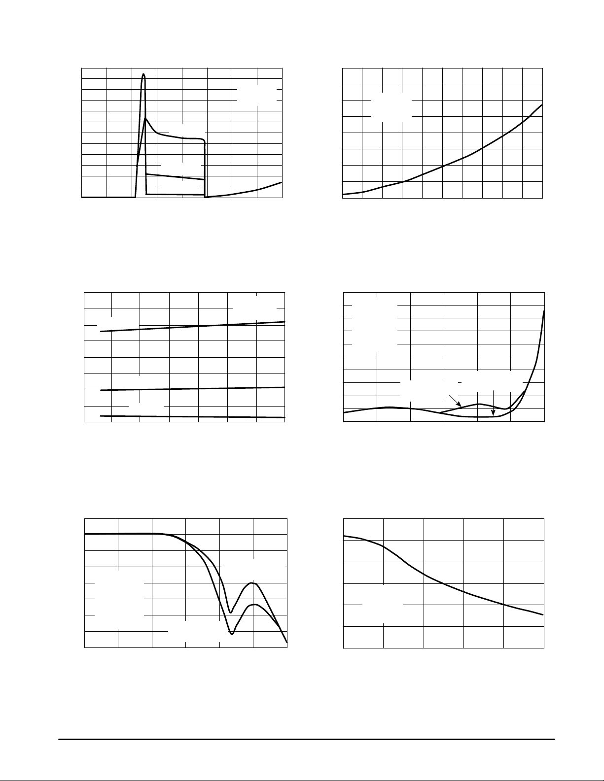
Figure 7. Bias Current versus Input Voltage
12
10
8.0
RL = 50
6.0
4.0
, BIAS CURRENT (mA)
B
I
2.0
0
–20 –10 0 10 20 30 40 50 60
RL = 100
RL = 500
Vin, INPUT VOLTAGE (V)
Ω
Ω
Ω
V
= 5.0 V
out
TJ = 25
°
C
Figure 8. Bias Current versus Output Current
8.0
6.0
4.0
, BIAS CURRENT (mA)
B
I
2.0
0
0 20 40 60 80 100
Vin = 14 V
V
= 5.0 V
out
°
C
TJ = 25
IO, OUTPUT CURRENT (mA)
Figure 9. Bias Current versus Junction T emperature Figure 10. Output Impedance versus Frequency
8.0
Vin = 14 V
V
= 5.0 V
IO = 100 mA
6.0
4.0
, BIAS CURRENT (mA)
B
2.0
I
0
–55 –25 0 25 50 75 100 125
IO = 50 mA
IO = 0 mA
TJ, JUNCTION TEMPERATURE (°C)
out
2.0
Vin = 14 V
V
= 5.0 V
Ω
, OUTPUT IMPEDANCE ( )
O
I
out
1.6
IO = 10 mA
DIO = 1.0 mA
µ
CO = 100
1.2
TJ = 25
0.8
0.4
0
10 100 1.0 k 10 k 100 k 1.0 M 10 M
F
°
C
C
= 0.15
O(ESR)
C
= 0.3
O(ESR)
Electrolytic
f, FREQUENCY (Hz)
Ω
Tantulum
Ω
Figure 11. Ripple Rejection versus Frequency Figure 12. Ripple Rejection versus Output Current
95
85
C
= 0.15
O(ESR)
Vin = 14 V
75
V
= 5.0 V
out
DVin = 100 mV
Ω
RL = 500
CO = 100 µF
65
RR, RIPPLE REJECTION RATIO (dB)
55
10 100 1.0 k 1.0 M 10 M
TJ = 25
°
C
C
= 0.3
O(ESR)
Electrolytic
10 k 100 k
f, FREQUENCY (Hz)
Tantulum
Ω
6
Ω
95
85
Vin = 14 V
V
= 5.0 V
75
RR, RIPPLE REJECTION RATIO (dB)
65
out
f = 120 Hz
°
C
TJ = 25
0 20 40 60 80 100
IO, OUTPUT CURRENT (mA)
MOTOROLA ANALOG IC DEVICE DATA
Page 7
LM2931 Series
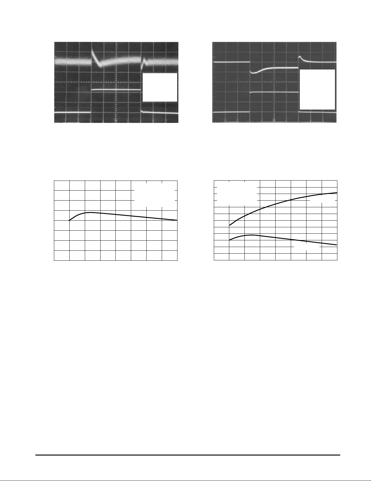
Figure 13. Line Regulation
, (2.0 mV/DIV)V
O
∆
18.5
OUTPUT VOLTAGE DEVIATION,
14
in
V , (V)
INPUT VOLTAGE,
t, TIME (10
µ
s/DIV)
V
= 5.0 V
out
RL = 500
CO = 100 µF
C
O(ESR)
TA = 25°C
Figure 15. Reference V oltage versus Output Voltage
1.240
LM2931C Adjustable
IO = 10 mA
Vin = V
+ 1.0 V
1.220
TA = 25
out
°
C
Ω
= 0.3
Figure 14. Load Regulation
, (2.0 mV/DIV)V
O
∆
Ω
OUTPUT VOLTAGE DEVIATION,
100
out
I (mA)
OUTPUT CURRENT,
0
µ
t, TIME (10
s/DIV)
Vin = 14 V
V
= 5.0 V
out
Cin = 1000
CO = 100 µF
C
= 0.3
O(ESR)
TA = 25°C
µ
F
Ω
Figure 16. Output Inhibit–Thresholds
versus Output Voltage
2.6
LM2931C Adjustable
IO = 10 mA
2.5
Vin = V
+ 1.0 V
2.4
TA = 25
out
°
C
Output “Off”
1.200
, REFERENCE VOLTAGE (V)
1.180
ref
V
1.160
0 3.0 6.0 9.0 12 15 18 21 24
VO, OUTPUT VOLTAGE (V)
APPLICATIONS INFORMATION
The LM2931 series regulators are designed with many
protection features making them essentially blow–out proof.
These features include internal current limiting, thermal
shutdown, overvoltage and reverse polarity input protection,
and the capability to withstand temporary power–up with
mirror–image insertion. Typical application circuits for the
fixed and adjustable output device are shown in Figures 17
and 18.
The input bypass capacitor Cin is recommended if the
regulator is located an appreciable distance (≥ 4″) from the
supply input filter. This will reduce the circuit’s sensitivity to
the input line impedance at high frequencies.
This regulator series is not internally compensated and
thus requires an external output capacitor for stability. The
capacitance value required is dependent upon the load
current, output voltage for the adjustable regulator, and the
type of capacitor selected. The least stable condition is
encountered at maximum load current and minimum output
voltage. Figure 22 shows that for operation in the “Stable”
region, under the conditions specified, the magnitude of the
output capacitor impedance |ZO| must not exceed 0.4 Ω. This
limit must be observed over the entire operating temperature
range of the regulator circuit.
2.3
2.2
, OUTPUT INHIBIT-THRESHOLDS (V)
2.1
2.0
th(on/off)
0 3.0 6.0 9.0 12 15 18 21 24
V
VO, OUTPUT VOLTAGE (V)
Output “On”
With economical electrolytic capacitors, cold temperature
operation can pose a serious stability problem. As the
electrolyte freezes, around –30°C, the capacitance will
decrease and the equivalent series resistance (ESR) will
increase drastically, causing the circuit to oscillate. Quality
electrolytic capacitors with extended temperature ranges of
–40° to +85°C and –55° to +105°C are readily available.
Solid tantalum capacitors may be a better choice if small size
is a requirement, however, the maximum ZO limit over
temperature must be observed.
Note that in the stable region, the output noise voltage is
linearly proportional to ZO. In effect, CO dictates the high
frequency roll–off point of the circuit. Operation in the area
titled “Marginally Stable” will cause the output of the regulator
to exhibit random bursts of oscillation that decay in an
under–damped fashion. Continuous oscillation occurs when
operating in the area titled “Unstable”. It is suggested that
oven testing of the entire circuit be performed with maximum
load, minimum input voltage, and minimum ambient
temperature.
MOTOROLA ANALOG IC DEVICE DATA
7
Page 8

LM2931 Series
Figure 17. Fixed Output Regulator Figure 18. Adjustable Output Regulator
Input
≥
6.0 V
V
in
C
in
0.1
Input
LM2931–5.0
Fixed
Output
Gnd
I
B
Figure 19. (5.0 A) Low Differential
V oltage Regulator
D45VH7
R
68
LM2931–5.0
+
100
Output
100
V
out
C
O
5.0 V @ 5.0 A
Output
+
V
in
Input
OutputInput
R
2
R
1
LM2931C
Adjustable
Output
I
B
Ǔ
)
I
Adj
Gnd
R
2
Adjust
I
22.5 k
51 k
Output
Inhibit
C
0.1
V
2
in
1
Switch Position 1 = Output “On”, 2 = Output “Off”
ǒ
+
V
1
ref
)
out
Figure 20. Current Boost Regulator with
Short Circuit Projection
R
SC
R
LM2931–5.0
++
100 100
Adj
V
out
R
1
C
O
R
2
R1R
w
2
R
)
R
1
2
Output
The LM2931 series can be current boosted with a PNP transistor. The
D45VH7, on a heatsink, will provide an output current of 5.0 A with an input
to output voltage differential of approximately 1.0 V. Resistor R in
conjunction with the VBE of the PNP determines when the pass transistor
begins conducting. This circuit is not short circuit proof.
The circuit of Figure 19 can be modified to provide supply protection against
short circuits by adding the current sense resistor RSC and an additional PNP
transistor. The current sensing PNP must be capable of handling the short
circuit current of the LM2931. Safe operating area of both transistors must be
considered under worst case conditions.
Figure 21. Constant Intensity Lamp Flasher Figure 22. Output Noise Voltage versus
Output Capacitor Impedance
Input
6.4 V to 30 V
100
100
f
= 2.2 Hz
osc
+
CM
#345
LM2931C
+
33 k
2.0 k
8.2 k
6.2 V
0
100
Vin = 5.6 V
V
= 5.0 V
out
IO = 100 mA
10
Vnrms 10 Hz to 10 MHz
|ZO| @ 40 kHz
°
C
TA = 25
1.0
0.1
, OUTPUT NOISE VOL TAGE (mVrms)
n
V
0.01
10 100 1.0 k 10 k
|ZO|, MAGNITUDE OF CAPACIT OR IMPEDANCE (mΩ)
Unstable
Marginally
Stable
Stable
8
MOTOROLA ANALOG IC DEVICE DATA
Page 9
LM2931 Series
Figure 23. SOP–8 Thermal Resistance and Maximum
Power Dissipation versus P.C.B. Copper Length
170 3.2
150
°
130
110
90
70
JA
JUNCTION–TO–AIR ( C/W)
θ
R , THERMAL RESISTANCE
50
30
02030504010
R
θ
JA
L, LENGTH OF COPPER (mm)
P
for TA = 50°C
D(max)
Graph represents symmetrical layout
2.0 oz.
L
Copper
Figure 24. DP AK Thermal Resistance and Maximum
Power Dissipation versus P.C.B. Copper Length
°
100
90
80
70
Free Air
Mounted
Vertically
Minimum
Size Pad
P
D(max)
for TA = 50°C
2.0 oz. Copper
L
2.8
2.4
2.0
1.6
3.0 mmL
L
1.2
0.8
0.4
2.4
2.0
1.6
1.2
, MAXIMUM POWER DISSIPATION (W)
D
P
60
JA
JUNCTION–TO–AIR ( C/W)
θ
R , THERMAL RESISTANCE
50
40
010203025155.0
80
70
°
60
50
JA
JUNCTION–TO–AIR ( C/W)
θ
40
R , THERMAL RESISTANCE
30
010203025155.0
R
θ
JA
L, LENGTH OF COPPER (mm)
Figure 25. 3–Pin and 5–Pin D2PAK
Thermal Resistance and Maximum Power
Dissipation versus P.C.B. Copper Length
P
for TA = 50°C
D(max)
Free Air
Mounted
Vertically
Minimum
Size Pad
R
L, LENGTH OF COPPER (mm)
θ
JA
2.0 oz. Copper
L
L
0.8
0.4
0
3.5
3.0
2.5
2.0
1.5
1.0
, MAXIMUM POWER DISSIPATION (W)
D
P
, MAXIMUM POWER DISSIPATION (W)
D
P
MOTOROLA ANALOG IC DEVICE DATA
9
Page 10

LM2931 Series
DEFINITIONS
Dropout V oltage – The input/output voltage dif ferential at
which the regulator output no longer maintains regulation
against further reductions in input voltage. Measured when
the output decreases 100 mV from nominal value at 14 V
input, dropout voltage is affected by junction temperature and
load current.
Line Regulation – The change in output voltage for a
change in the input voltage. The measurement is made under
conditions of low dissipation or by using pulse techniques
such that the average chip temperature is not significantly
affected.
Load Regulation – The change in output voltage for a
change in load current at constant chip temperature.
Maximum Power Dissipation – The maximum total
device dissipation for which the regulator will operate within
specifications.
Bias Current – That part of the input current that is not
delivered to the load.
Output Noise Voltage – The rms AC voltage at the
output, with constant load and no input ripple, measured over
a specified frequency range.
Long–Term Stabliity – Output voltage stability under
accelerated life test conditions with the maximum rated
voltage listed in the devices electrical characteristics and
maximum power dissipation.
10
MOTOROLA ANALOG IC DEVICE DATA
Page 11
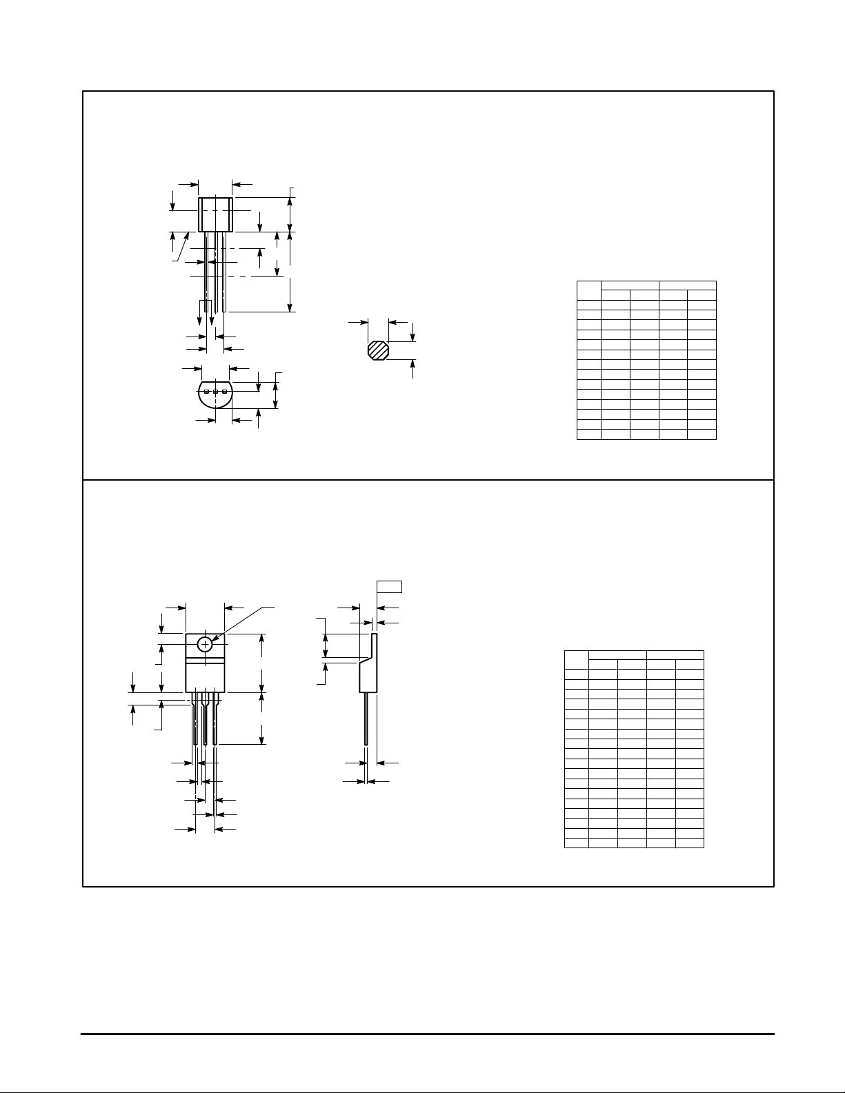
SEATING
PLANE
R
XX
A
H
V
1
N
P
F
G
N
LM2931 Series
OUTLINE DIMENSIONS
Z SUFFIX
PLASTIC PACKAGE
CASE 29–04
(TO–92 Type)
ISSUE AD
B
L
K
D
J
C
SECTION X–X
NOTES:
1. DIMENSIONING AND TOLERANCING PER ANSI
Y14.5M, 1982.
2. CONTROLLING DIMENSION: INCH.
3. CONTOUR OF PACKAGE BEYOND DIMENSION R
IS UNCONTROLLED.
4. DIMENSION F APPLIES BETWEEN P AND L.
DIMENSION D AND J APPLY BETWEEN L AND K
MINIMUM. LEAD DIMENSION IS UNCONTROLLED
IN P AND BEYOND DIMENSION K MINIMUM.
INCHES MILLIMETERS
MIN MINMAX MAX
DIM
A
B
C
D
G
H
K
N
P
R
V
F
J
L
0.175
0.170
0.125
0.016
0.016
0.045
0.095
0.015
0.500
0.250
0.080
–
0.115
0.135
0.205
0.210
0.165
0.022
0.019
0.055
0.105
0.020
–
–
0.105
0.100
–
–
4.45
4.32
3.18
0.41
0.41
1.15
2.42
0.39
12.70
6.35
2.04
–
2.93
3.43
5.20
5.33
4.19
0.55
0.48
1.39
2.66
0.50
2.66
2.54
–
–
–
–
T SUFFIX
PLASTIC PACKAGE
CASE 221A–06
(TO–220 Type)
ISSUE Y
SEATING
–T–
PLANE
B
4
Q
123
F
T
C
S
A
U
H
K
Z
L
V
R
J
G
D
N
NOTES:
1. DIMENSIONING AND TOLERANCING PER ANSI
Y14.5M, 1982.
2. CONTROLLING DIMENSION: INCH.
3. DIM Z DEFINES A ZONE WHERE ALL BODY AND
LEAD IRREGULARITIES ARE ALLOWED.
INCHES MILLIMETERS
MIN MINMAX MAX
DIM
A
B
C
D
F
G
H
J
K
L
N
Q
R
S
T
U
V
Z
0.570
0.380
0.160
0.025
0.142
0.095
0.110
0.018
0.500
0.045
0.190
0.100
0.080
0.045
0.235
0.000
0.045
–
0.620
0.405
0.190
0.035
0.147
0.105
0.155
0.025
0.562
0.060
0.210
0.120
0.110
0.055
0.255
0.050
–
0.080
14.48
9.66
4.07
0.64
3.61
2.42
2.80
0.46
12.70
1.15
4.83
2.54
2.04
1.15
5.97
0.00
1.15
15.75
10.28
4.82
0.88
3.73
2.66
3.93
0.64
14.27
1.52
5.33
3.04
2.79
1.39
6.47
1.27
–
2.04
–
MOTOROLA ANALOG IC DEVICE DATA
11
Page 12

LM2931 Series
OUTLINE DIMENSIONS
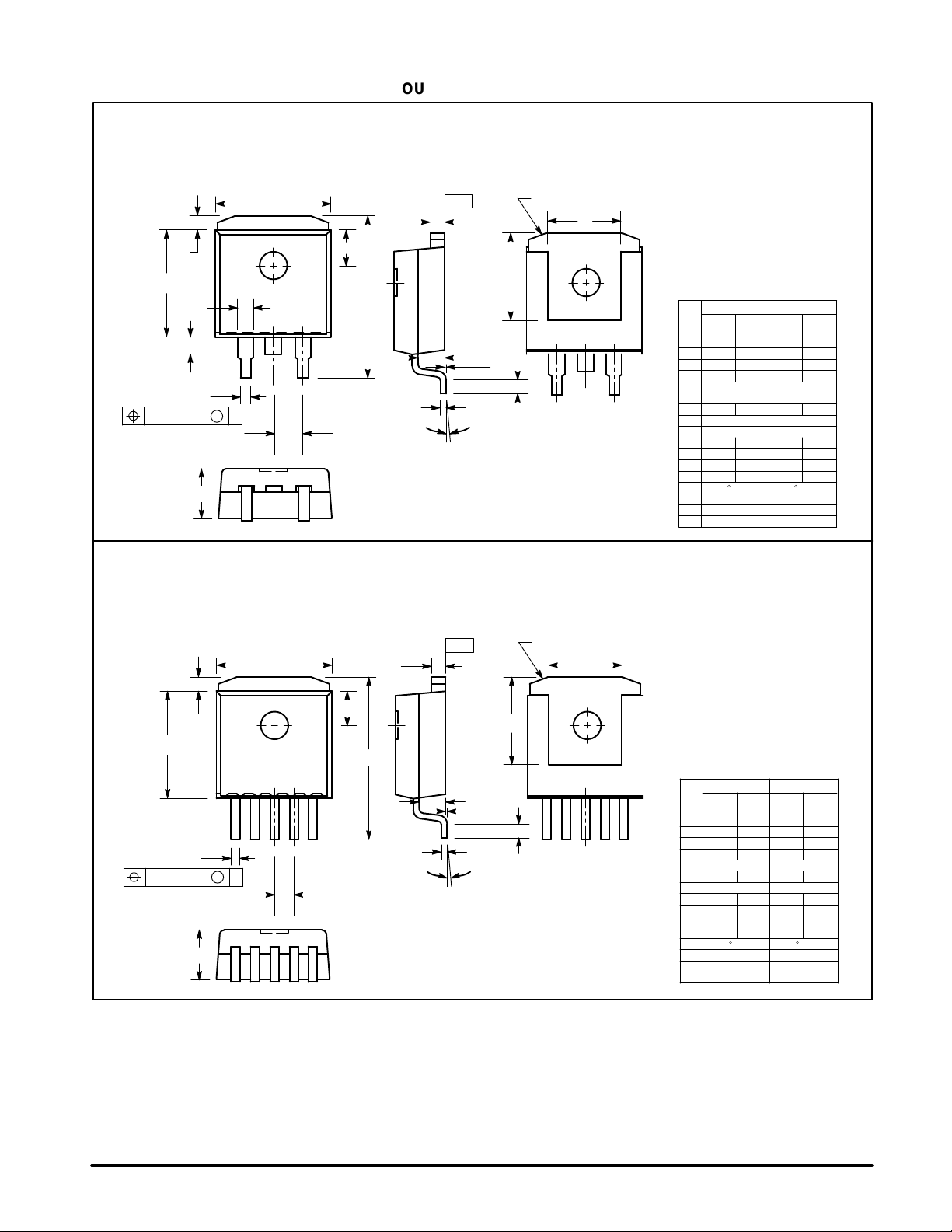
TH SUFFIX
PLASTIC PACKAGE
CASE 314A–03
(TO–220 Type)
ISSUE D
Q
D 5 PL
Q
U
–P–
B
12345
M M
B
–P–
SEATING
–T–
PLANE
C
OPTIONAL
CHAMFER
A
G
E
L
F
K
J 5 PL
S
TP0.014 (0.356)
NOTES:
1. DIMENSIONING AND TOLERANCING PER ANSI
Y14.5M, 1982.
2. CONTROLLING DIMENSION: INCH.
3. DIMENSION D DOES NOT INCLUDE
INTERCONNECT BAR (DAMBAR) PROTRUSION.
DIMENSION D INCLUDING PROTRUSION SHALL
NOT EXCEED 0.043 (1.092) MAXIMUM.
INCHES
DIMAMIN MAX MIN MAX
0.572 0.613 14.529 15.570
B 0.390 0.415 9.906 10.541
C 0.170 0.180 4.318 4.572
D 0.025 0.038 0.635 0.965
E 0.048 0.055 1.219 1.397
F 0.570 0.585 14.478 14.859
G 0.067 BSC 1.702 BSC
J 0.015 0.025 0.381 0.635
K 0.730 0.745 18.542 18.923
L 0.320 0.365 8.128 9.271
Q 0.140 0.153 3.556 3.886
S 0.210 0.260 5.334 6.604
U 0.468 0.505 11.888 12.827
MILLIMETERS
TV SUFFIX
PLASTIC PACKAGE
CASE 314B–05
(TO–220 Type)
ISSUE J
NOTES:
C
E
1. DIMENSIONING AND TOLERANCING PER ANSI Y14.5M, 1982.
2. CONTROLLING DIMENSION: INCH.
3. DIMENSION D DOES NOT INCLUDE INTERCONNECT BAR
(DAMBAR) PROTRUSION. DIMENSION D INCLUDING
PROTRUSION SHALL NOT EXCEED 0.043 (1.092) MAXIMUM.
12
U
F
K
12345
A
L
S
V
W
DIM
J 5 PL
D 5 PL
M M
TP0.10 (0.254)
G
0.24 (0.610)
M
T
H
N
SEATING
–T–
PLANE
INCHES MILLIMETERS
MIN MINMAX MAX
A
0.572
0.390
0.170
0.025
0.048
0.850
0.015
0.900
0.320
0.140
–
0.468
–
0.090
0.613
0.415
0.180
0.038
0.055
0.935
0.025
1.100
0.365
0.153
0.620
0.505
0.735
0.110
B
C
D
E
F
G
H
J
K
L
N
Q
S
U
V
W
14.529
9.906
4.318
0.635
1.219
21.590
1.702 BSC0.067 BSC
4.216 BSC0.166 BSC
0.381
22.860
8.128
8.128 BSC0.320 BSC
3.556
–
11.888
–
2.286
15.570
10.541
4.572
0.965
1.397
23.749
0.635
27.940
9.271
3.886
15.748
12.827
18.669
2.794
MOTOROLA ANALOG IC DEVICE DATA
Page 13

–Q–
U
K
5 PL
D
0.356 (0.014) T Q
B
12345
M M
LM2931 Series
OUTLINE DIMENSIONS
T SUFFIX
PLASTIC PACKAGE
CASE 314D–03
(TO–220 Type)
ISSUE D
SEATING
–T–
PLANE
C
E
A
L
S
G
J
H
NOTES:
1. DIMENSIONING AND TOLERANCING PER ANSI
Y14.5M, 1982.
2. CONTROLLING DIMENSION: INCH.
3. DIMENSION D DOES NOT INCLUDE
INTERCONNECT BAR (DAMBAR) PROTRUSION.
DIMENSION D INCLUDING PROTRUSION SHALL
NOT EXCEED 10.92 (0.043) MAXIMUM.
INCHES MILLIMETERS
MIN MINMAX MAX
DIM
A
B
C
D
E
G
H
K
Q
U
S
J
L
0.572
0.390
0.170
0.025
0.048
0.087
0.015
1.020
0.320
0.140
0.105
0.543
0.613
0.415
0.180
0.038
0.055
0.112
0.025
1.065
0.365
0.153
0.117
0.582
14.529
9.906
4.318
0.635
1.219
1.702 BSC0.067 BSC
2.210
0.381
25.908
8.128
3.556
2.667
13.792
15.570
10.541
4.572
0.965
1.397
2.845
0.635
27.051
9.271
3.886
2.972
14.783
V
–T–
SEATING
PLANE
S
F
B
R
4
123
G
A
K
3 PL
D
0.13 (0.005) T
DT–1 SUFFIX
PLASTIC PACKAGE
CASE 369–07
(DPAK)
ISSUE L
C
E
J
H
M
NOTES:
1. DIMENSIONING AND TOLERANCING PER ANSI
Y14.5M, 1982.
2. CONTROLLING DIMENSION: INCH.
DIM MIN MAX MIN MAX
A 0.235 0.250 5.97 6.35
B 0.250 0.265 6.35 6.73
C 0.086 0.094 2.19 2.38
D 0.027 0.035 0.69 0.88
E 0.033 0.040 0.84 1.01
F 0.037 0.047 0.94 1.19
0.090 BSC 2.29 BSC
G
H 0.034 0.040 0.87 1.01
J 0.018 0.023 0.46 0.58
K 0.350 0.380 8.89 9.65
R 0.175 0.215 4.45 5.46
S 0.050 0.090 1.27 2.28
V 0.030 0.050 0.77 1.27
MILLIMETERSINCHES
MOTOROLA ANALOG IC DEVICE DATA
13
Page 14

LM2931 Series
OUTLINE DIMENSIONS
DT SUFFIX
PLASTIC PACKAGE
CASE 369A–13
(DPAK)
ISSUE Y
SEATING
–T–
PLANE
B
V
S
R
4
A
123
K
F
L
D
2 PL
G
0.13 (0.005) T
C
E
Z
U
J
H
M
DIM MIN MAX MIN MAX
A 0.235 0.250 5.97 6.35
B 0.250 0.265 6.35 6.73
C 0.086 0.094 2.19 2.38
D 0.027 0.035 0.69 0.88
E 0.033 0.040 0.84 1.01
F 0.037 0.047 0.94 1.19
G 0.180 BSC 4.58 BSC
H 0.034 0.040 0.87 1.01
J 0.018 0.023 0.46 0.58
K 0.102 0.114 2.60 2.89
L 0.090 BSC 2.29 BSC
R 0.175 0.215 4.45 5.46
S 0.020 0.050 0.51 1.27
U 0.020 ––– 0.51 –––
V 0.030 0.050 0.77 1.27
Z 0.138 ––– 3.51 –––
MILLIMETERSINCHES
D SUFFIX
PLASTIC PACKAGE
CASE 751–05
(SOP–8)
ISSUE S
A
E
B
C
A1
D
58
0.25MB
1
H
4
e
M
h
X 45
_
q
C
A
SEATING
PLANE
0.10
L
B
SS
A0.25MCB
NOTES:
1. DIMENSIONING AND TOLERANCING PER ASME
Y14.5M, 1994.
2. DIMENSIONS ARE IN MILLIMETERS.
3. DIMENSION D AND E DO NOT INCLUDE MOLD
PROTRUSION.
4. MAXIMUM MOLD PROTRUSION 0.15 PER SIDE.
5. DIMENSION B DOES NOT INCLUDE MOLD
PROTRUSION. ALLOWABLE DAMBAR
PROTRUSION SHALL BE 0.127 TOTAL IN EXCESS
OF THE B DIMENSION AT MAXIMUM MATERIAL
CONDITION.
MILLIMETERS
DIM MIN MAX
A 1.35 1.75
A1 0.10 0.25
B 0.35 0.49
C 0.18 0.25
D 4.80 5.00
E
3.80 4.00
1.27 BSCe
H 5.80 6.20
h
0.25 0.50
L 0.40 1.25
0 7
q
__
14
MOTOROLA ANALOG IC DEVICE DATA
Page 15
K
B
F
J
D
0.010 (0.254) T
M
C
A
12 3
G
S
H
LM2931 Series
OUTLINE DIMENSIONS
D2T SUFFIX
PLASTIC PACKAGE
CASE 936–03
(D2PAK)
ISSUE B
–T–
E
V
M
L
P
N
R
TERMINAL 4
U
NOTES:
1 DIMENSIONING AND TOLERANCING PER ANSI
Y14.5M, 1982.
2 CONTROLLING DIMENSION: INCH.
3 TAB CONTOUR OPTIONAL WITHIN DIMENSIONS
A AND K.
4 DIMENSIONS U AND V ESTABLISH A MINIMUM
MOUNTING SURFACE FOR TERMINAL 4.
5 DIMENSIONS A AND B DO NOT INCLUDE MOLD
FLASH OR GATE PROTRUSIONS. MOLD FLASH
AND GATE PROTRUSIONS NOT TO EXCEED
0.025 (0.635) MAXIMUM.
INCHES
DIMAMIN MAX MIN MAX
0.386 0.403 9.804 10.236
B 0.356 0.368 9.042 9.347
C 0.170 0.180 4.318 4.572
D 0.026 0.036 0.660 0.914
E 0.045 0.055 1.143 1.397
F 0.051 REF 1.295 REF
G 0.100 BSC 2.540 BSC
H 0.539 0.579 13.691 14.707
J 0.125 MAX 3.175 MAX
K 0.050 REF 1.270 REF
L 0.000 0.010 0.000 0.254
M 0.088 0.102 2.235 2.591
N 0.018 0.026 0.457 0.660
P 0.058 0.078 1.473 1.981
__
R
S 0.116 REF 2.946 REF
U 0.200 MIN 5.080 MIN
V 0.250 MIN 6.350 MIN
MILLIMETERS
5 REF5 REF
K
B
D
0.010 (0.254) T
M
C
A
123
G
45
S
H
D2T SUFFIX
PLASTIC PACKAGE
CASE 936A–02
–T–
E
N
(D2PAK)
ISSUE A
M
R
L
V
P
TERMINAL 6
NOTES:
6 DIMENSIONING AND TOLERANCING PER ANSI
U
Y14.5M, 1982.
7 CONTROLLING DIMENSION: INCH.
8 TAB CONTOUR OPTIONAL WITHIN DIMENSIONS
A AND K.
9 DIMENSIONS U AND V ESTABLISH A MINIMUM
MOUNTING SURFACE FOR TERMINAL 6.
10 DIMENSIONS A AND B DO NOT INCLUDE MOLD
FLASH OR GATE PROTRUSIONS. MOLD FLASH
AND GATE PROTRUSIONS NOT TO EXCEED
0.025 (0.635) MAXIMUM.
INCHES
DIMAMIN MAX MIN MAX
0.386 0.403 9.804 10.236
B 0.356 0.368 9.042 9.347
C 0.170 0.180 4.318 4.572
D 0.026 0.036 0.660 0.914
E 0.045 0.055 1.143 1.397
G 0.067 BSC 1.702 BSC
H 0.539 0.579 13.691 14.707
K 0.050 REF 1.270 REF
L 0.000 0.010 0.000 0.254
M 0.088 0.102 2.235 2.591
N 0.018 0.026 0.457 0.660
P 0.058 0.078 1.473 1.981
__
R 5 REF
S 0.116 REF 2.946 REF
U 0.200 MIN 5.080 MIN
V 0.250 MIN 6.350 MIN
MILLIMETERS
5 REF
MOTOROLA ANALOG IC DEVICE DATA
15
Page 16

LM2931 Series
Motorola reserves the right to make changes without further notice to any products herein. Motorola makes no warranty , representation or guarantee regarding
the suitability of its products for any particular purpose, nor does Motorola assume any liability arising out of the application or use of any product or circuit, and
specifically disclaims any and all liability, including without limitation consequential or incidental damages. “T ypical” parameters which may be provided in Motorola
data sheets and/or specifications can and do vary in different applications and actual performance may vary over time. All operating parameters, including “Typicals”
must be validated for each customer application by customer’s technical experts. Motorola does not convey any license under its patent rights nor the rights of
others. Motorola products are not designed, intended, or authorized for use as components in systems intended for surgical implant into the body, or other
applications intended to support or sustain life, or for any other application in which the failure of the Motorola product could create a situation where personal injury
or death may occur. Should Buyer purchase or use Motorola products for any such unintended or unauthorized application, Buyer shall indemnify and hold Motorola
and its officers, employees, subsidiaries, affiliates, and distributors harmless against all claims, costs, damages, and expenses, and reasonable attorney fees
arising out of, directly or indirectly, any claim of personal injury or death associated with such unintended or unauthorized use, even if such claim alleges that
Motorola was negligent regarding the design or manufacture of the part. Motorola and are registered trademarks of Motorola, Inc. Motorola, Inc. is an Equal
Opportunity/Affirmative Action Employer.
How to reach us:
USA/EUROPE/Locations Not Listed: Motorola Literature Distribution; JAPAN: Nippon Motorola Ltd.: SPD, Strategic Planning Office, 4–32–1,
P.O. Box 5405, Denver, Colorado 80217. 303–675–2140 or 1–800–441–2447 Nishi–Gotanda, Shinagawa–ku, Tokyo 141, Japan. 81–3–5487–8488
Mfax: RMFAX0@email.sps.mot.com – TOUCHTONE 602–244–6609 ASIA/PACIFIC: Motorola Semiconductors H.K. Ltd.; 8B Tai Ping Industrial Park,
INTERNET: http://motorola.com/sps
16
– US & Canada ONLY 1–800–774–1848 51 Ting Kok Road, Tai Po, N.T., Hong Kong. 852–26629298
◊
MOTOROLA ANALOG IC DEVICE DATA
Mfax is a trademark of Motorola, Inc.
LM2931/D
 Loading...