

Utilizing the circuit designs perfected for recently introduced Quad
Operational Amplifiers, these dual operational amplifiers feature 1) low
power drain, 2) a common mode input voltage range extending to
ground/VEE, 3) single supply or split supply operation and 4) pinouts
compatible with the popular MC1558 dual operational amplifier. The LM158
series is equivalent to one–half of an LM124.
These amplifiers have several distinct advantages over standard
operational amplifier types in single supply applications. They can operate at
supply voltages as low as 3.0 V or as high as 32 V, with quiescent currents
about one–fifth of those associated with the MC1741 (on a per amplifier
basis). The common mode input range includes the negative supply , thereby
eliminating the necessity for external biasing components in many
applications. The output voltage range also includes the negative power
supply voltage.
• Short Circuit Protected Outputs
• True Differential Input Stage
• Single Supply Operation: 3.0 V to 32 V
• Low Input Bias Currents
• Internally Compensated
• Common Mode Range Extends to Negative Supply
• Single and Split Supply Operation
• Similar Performance to the Popular MC1558
• ESD Clamps on the Inputs Increase Ruggedness of the Device without
Affecting Operation
Order this document by LM358/D
DUAL DIFFERENTIAL INPUT
OPERATIONAL AMPLIFIERS
SEMICONDUCTOR
TECHNICAL DATA
8
1
N SUFFIX
PLASTIC PACKAGE
CASE 626
8
1
D SUFFIX
PLASTIC PACKAGE
CASE 751
(SO–8)
MAXIMUM RATINGS (T
Rating
Power Supply Voltages Vdc
Single Supply V
Split Supplies VCC, V
Input Differential Voltage
Range (Note 1)
Input Common Mode Voltage
Range (Note 2)
Output Short Circuit Duration t
Junction Temperature T
Storage Temperature Range T
Operating Ambient Temperature
Range
LM258 –25 to +85 –
LM358 0 to +70 –
LM2904 – –40 to +105
LM2904V – –40 to +125
NOTES: 1.Split Power Supplies.
2.For Supply Voltages less than 32 V for the LM258/358 and 26 V for the LM2904, the
absolute maximum input voltage is equal to the supply voltage.
= +25°C, unless otherwise noted.)
A
LM258
Symbol
CC
V
IDR
V
ICR
SC
J
stg
T
A
LM358
32 26
EE
±16 ±13
±32 ±26 Vdc
–0.3 to 32 –0.3 to 26 Vdc
Continuous
–55 to +125 °C
LM2904
LM2904V
150 °C
MOTOROLA ANALOG IC DEVICE DATA
Unit
°C
PIN CONNECTIONS
Output A
Inputs A
VEE/Gnd
1
2
–
+
3
4
(Top View)
–
+
8
V
CC
7
Output B
6
5
Inputs B
ORDERING INFORMATION
Operating
Device
LM2904D
LM2904N
LM2904VD
LM2904VN
LM258D
LM258N
LM358D
LM358N
Motorola, Inc. 1996 Rev 2
Temperature Range
TA = –40° to +105°C
TA = –40° to +125°C
TA = –25° to +85°C
TA = 0° to +70°C
Package
SO–8
Plastic DIP
SO–8
Plastic DIP
SO–8
Plastic DIP
SO–8
Plastic DIP
1
LM358, LM258, LM2904, LM2904V
ELECTRICAL CHARACTERISTICS (V
= 5.0 V, VEE = Gnd, TA = 25°C, unless otherwise noted.)
CC
LM258 LM358 LM2904 LM2904V
Characteristic Symbol
Input Offset Voltage
VCC = 5.0 V to 30 V (26 V for
LM2904, V), VIC = 0 V to VCC –1.7 V,
VO ] 1.4 V, RS = 0 Ω
TA = 25°C – 2.0 5.0 – 2.0 7.0 – 2.0 7.0 – – –
TA = T
TA = T
Average Temperature Coefficient of Input
Offset Voltage
TA = T
Input Offset Current I
TA = T
Input Bias Current I
TA = T
Average Temperature Coefficient of Input
Offset Current
TA = T
Input Common Mode Voltage Range
(Note 2),VCC = 30 V (26 V for LM2904, V)
VCC = 30 V (26 V for LM2904, V),
Differential Input Voltage Range V
Large Signal Open Loop Voltage Gain A
RL = 2.0 kΩ, VCC = 15 V, For Large V
TA = T
Channel Separation CS – –120 – – –120 – – –120 – – –120 – dB
1.0 kHz ≤ f ≤ 20 kHz, Input Referenced
Common Mode Rejection
RS ≤ 10 kΩ
Power Supply Rejection PSR 65 100 – 65 100 – 50 100 – 50 100 – dB
Output Voltage–High Limit (TA = T
T
low
VCC = 5.0 V, RL = 2.0 kΩ, TA = 25°C 3.3 3.5 – 3.3 3.5 – 3.3 3.5 – 3.3 3.5 –
VCC = 30 V (26 V for LM2904, V),
VCC = 30 V (26 V for LM2904, V),
Output Voltage–Low Limit V
VCC = 5.0 V, RL = 10 kΩ, TA = T
Output Source Current I
VID = +1.0 V, VCC = 15 V
Output Sink Current I
VID = –1.0 V, VCC = 15 V 10 20 – 10 20 – 10 20 – 10 20 – mA
VID = –1.0 V, VO = 200 mV 12 50 – 12 50 – – – – – – – µA
Output Short Circuit to Ground (Note 3) I
Power Supply Current (TA = T
(Note 1)
VCC = 30 V (26 V for LM2904, V),
VCC = 5 V, VO = 0 V, RL = ∞ – 0.7 1.2 – 0.7 1.2 – 0.7 1.2 – 0.7 1.2
NOTES: 1.T
(Note 1) – – 7.0 – – 9.0 – – 10 – – 13
high
(Note 1) – – 2.0 – – 9.0 – – 10 – – 10
low
∆VIO/∆T – 7.0 – – 7.0 – – 7.0 – – 7.0 – µV/°C
to T
(Note 1)
low
to T
(Note 1) – – 100 – – 150 – 45 200 – 45 200
low
to T
(Note 1) – –50 –300 – –50 –500 – –50 –500 – –50 –500
low
∆IIO/∆T – 10 – – 10 – – 10 – – 10 – pA/°C
to T
(Note 1)
low
V
to T
low
O
to T
(Note 1) 25 – – 15 – – 15 – – 15 – –
low
TA = T
Swing,
high
high
high
high
high
high
CMR 70 85 – 65 70 – 50 70 – 50 70 – dB
to
low
V
to
)
high
high
high
to T
) (Note 1)
RL = 2.0 kΩ
RL = 10 kΩ
T
(Note 1)
low
VO = 0 V, RL = ∞
= –40°C for LM2904 T
low
= –40°C for LM2904V = +125°C for LM2904V
= –25°C for LM258 = +85°C for LM258
=0°C for LM358 = +70°C for LM358
2.The input common mode voltage or either input signal voltage should not be allowed to go negative by more than 0.3 V . The upper end of the common
mode voltage range is VCC –1.7 V.
3.Short circuits from the output to VCC can cause excessive heating and eventual destruction. Destructive dissipation can result from simultaneous shorts
on all amplifiers.
Min Typ Max Min Typ Max Min Typ Max Min Typ Max
V
IO
IO
IB
ICR
IDR
VOL
OH
OL
O+
O–
SC
I
CC
– 3.0 30 – 5.0 50 – 5.0 50 – 5.0 50 nA
– –45 –150 – –45 –250 – –45 –250 – –45 –250
0 – 28.3 0 – 28.3 0 – 24.3 0 – 24.3
0 – 28 0 – 28 0 – 24 0 – 24
– – V
50 100 – 25 100 – 25 100 – 25 100 –
26 – – 26 – – 22 – – 22 – –
27 28 – 27 28 – 23 24 – 23 24 –
– 5.0 20 – 5.0 20 – 5.0 20 – 5.0 20 mV
20 40 – 20 40 – 20 40 – 20 40 – mA
– 40 60 – 40 60 – 40 60 – 40 60 mA
– 1.5 3.0 – 1.5 3.0 – 1.5 3.0 – 1.5 3.0
= +105°C for LM2904
high
CC
– – V
CC
– – V
CC
– – V
CC
Unit
mV
V
V
V/mV
V
mA
2
MOTOROLA ANALOG IC DEVICE DATA
3.0 V to V
CC(max)
Q19
LM358, LM258, LM2904, LM2904V
Single Supply Split Supplies
Q16
V
CC
1
2
VEE/Gnd
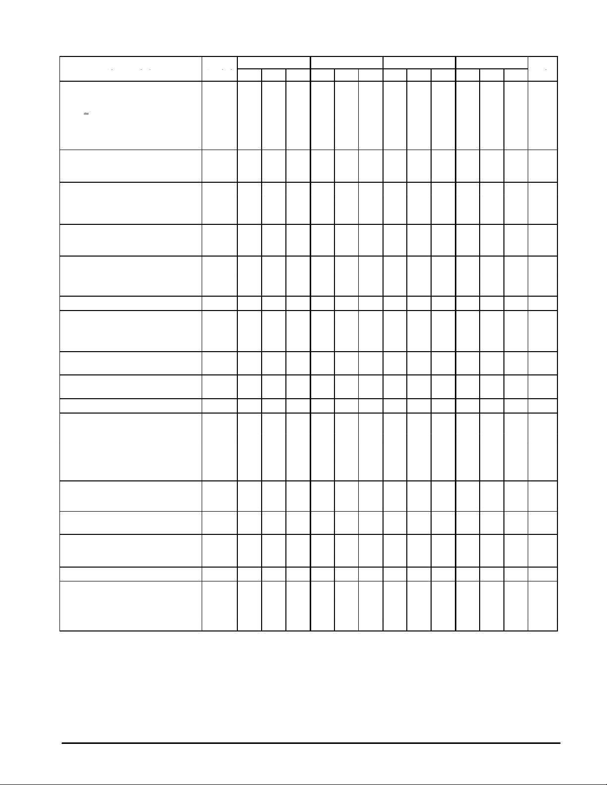
Representative Schematic Diagram
(One–Half of Circuit Shown)
Q15
Q14
40 k
Q13
V
CC
1
2
V
EE
Output
1.5 V to V
1.5 V to V
Bias Circuitry
Common to Both
Amplifiers
Q22
CC(max)
EE(max)
V
CC
5.0 pF
Q18
Inputs
Q17
Q2
Q3 Q4
Q20
Q21
Q5
Q6
Q26
Q9
Q7
Q8
CIRCUIT DESCRIPTION
The LM258 series is made using two internally
compensated, two–stage operational amplifiers. The first
stage of each consists of differential input devices Q20 and
Q18 with input buffer transistors Q21 and Q17 and the
differential to single ended converter Q3 and Q4. The first
stage performs not only the first stage gain function but also
performs the level shifting and transconductance reduction
functions. By reducing the transconductance, a smaller
compensation capacitor (only 5.0 pF) can be employed, thus
saving chip area. The transconductance reduction is
accomplished by splitting the collectors of Q20 and Q18.
Another feature of this input stage is that the input common
mode range can include the negative supply or ground, in
single supply operation, without saturating either the input
devices or the differential to single–ended converter. The
second stage consists of a standard current source load
amplifier stage.
Each amplifier is biased from an internal–voltage regulator
which has a low temperature coefficient thus giving each
amplifier good temperature characteristics as well as
excellent power supply rejection.
Q12
25
Q11
1.0 V/DIV
Q10
Q1
2.0 k
Large Signal V oltage
Follower Response
Q23
Q25
5.0 µs/DIV
2.4 k
Q24
VCC = 15 Vdc
RL = 2.0 k
TA = 25°C
VEE/Gnd
Ω
MOTOROLA ANALOG IC DEVICE DATA
3

LM358, LM258, LM2904, LM2904V
Figure 1. Input V oltage Range Figure 2. Large–Signal Open Loop V oltage Gain
20
18
16
14
12
10
8.0
I
6.0
V , INPUT VOL TAGE (V)
4.0
2.0
0
0 2.0 4.0 6.0 8.0 10 12 14 16 18 20
Figure 3. Large–Signal Frequency Response
14
pp
12
10
8.0
6.0
4.0
, OUTPUT VOLTAGE RANGE (V )
2.0
OR
V
0
1.0 10 100 1000
Negative
Positive
VCC/V
POWER SUPPLY VOLTAGES (V)
EE,
f, FREQUENCY (kHz)
RL = 2.0 k
VCC = 15 V
VEE = Gnd
Gain = –100
RI = 1.0 k
RF = 100 k
Ω
Ω
Ω
120
100
80
60
40
20
, OPEN LOOP VOL TAGE GAIN (dB)
0
VOL
A
–20
1.0 10 100 1.0 k 10 k 100 k 1.0 M
f, FREQUENCY (Hz)
VCC = 15 V
VEE = Gnd
°
TA = 25
Figure 4. Small Signal V oltage Follower
Pulse Response (Noninverting)
550
500
450
400
350
300
, OUTPUT VOL TAGE (mV)
O
250
V
200
0
0 1.0 2.0 3.0 4.0 5.0 6.0 7.0 8.0
Input
Output
t, TIME (ms)
VCC = 30 V
VEE = Gnd
TA = 25
CL = 50 pF
C
°
C
Figure 5. Power Supply Current versus
Power Supply Voltage
2.4
2.1
1.8
1.5
1.2
0.9
0.6
0.3
CC
I , POWER SUPPLY CURRENT (mA)
0
0 5.0 10 15 20 25 30 35
VCC, POWER SUPPLY VOLTAGE (V) VCC, POWER SUPPLY VOLTAGE (V)
TA = 25°C
RL =
4
R
Figure 6. Input Bias Current versus
Supply V oltage
90
80
IB
I , INPUT BIAS CURRENT (nA)
70
0 2.0 4.0 6.0 8.0 10 12 14 16 18 20
MOTOROLA ANALOG IC DEVICE DATA
LM358, LM258, LM2904, LM2904V
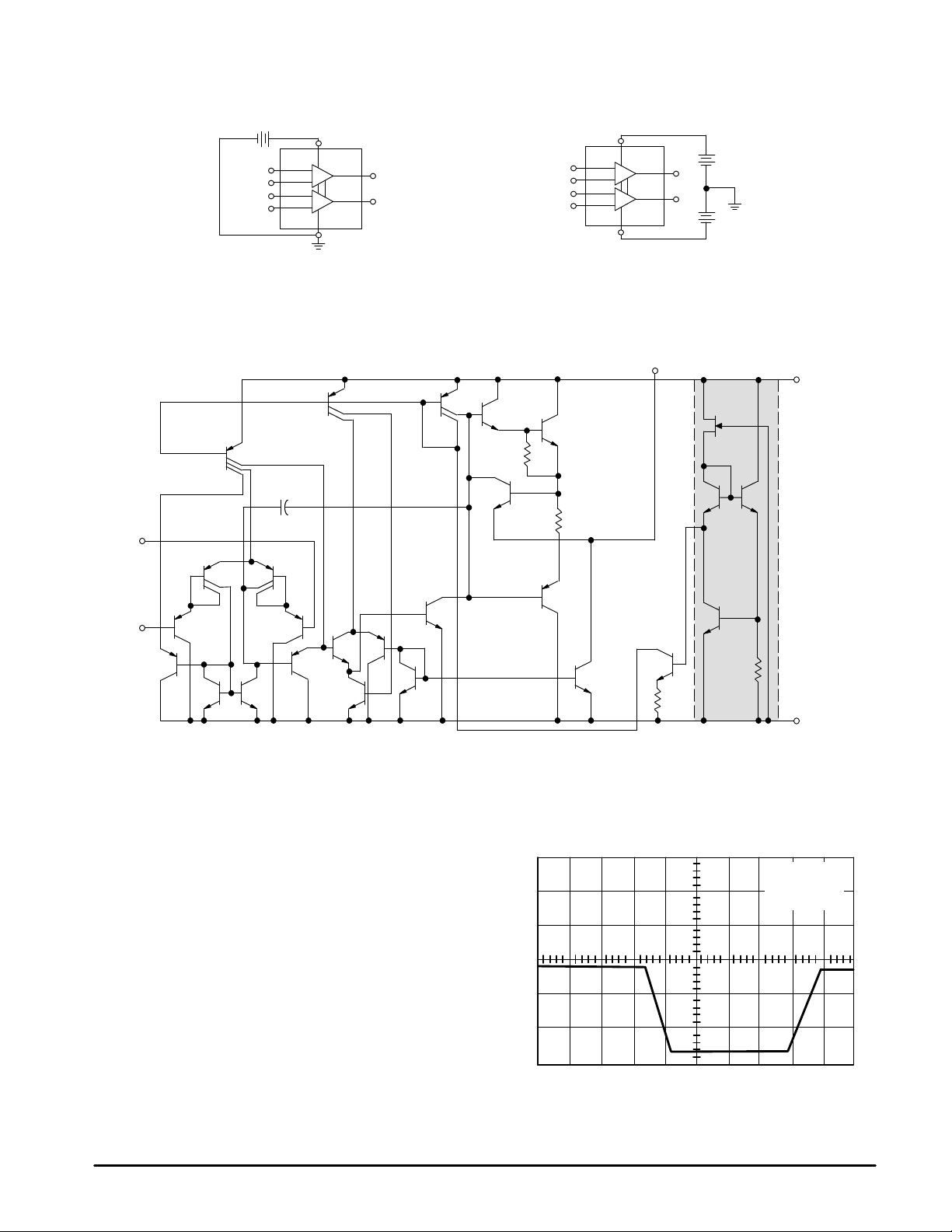
Figure 7. V oltage Reference Figure 8. Wien Bridge Oscillator
R1
V
V
CC
MC1403
R2
2.5 V
CC
–
1/2
LM358
+
VO = 2.5 V (1 +
R1
R2
10 k
CC
R
V
ref
V
ref
1
= V
2
V
O
)
Figure 9. High Impedance Differential Amplifier Figure 10. Comparator with Hysteresis
e
1
+
1/2
LM358
–
a R1
R1
b R1
–
1/2
LM358
e
2
+
eo = C (1 + a + b) (e2 – e1)
1
R
C
R
R2
–
1/2
LM358
e
o
+
1
R
C
R
R1
V
ref
V
in
+
1/2
LM358
–
R1
V
=
inL
R1 + R2
inH
=
H =
R1
R1 + R2
R1
R1 + R2
V
50 k
5.0 k
–
1/2
LM358
+
C
V
(VOL – V
(VOH – V
(VOH – VOL)
V
CC
V
fo =
For: fo = 1.0 kHz
R
C
Hysteresis
V
OH
V
O
O
V
ref
ref
OL
)+ V
) + V
V
ref
ref
O
1
π
RC
2
R = 16 k
C = 0.01 µF
inLVinH
V
ref
Ω
R
C1
V
in
R2
C
–
1/2
LM358
+
V
ref
R2
MOTOROLA ANALOG IC DEVICE DATA
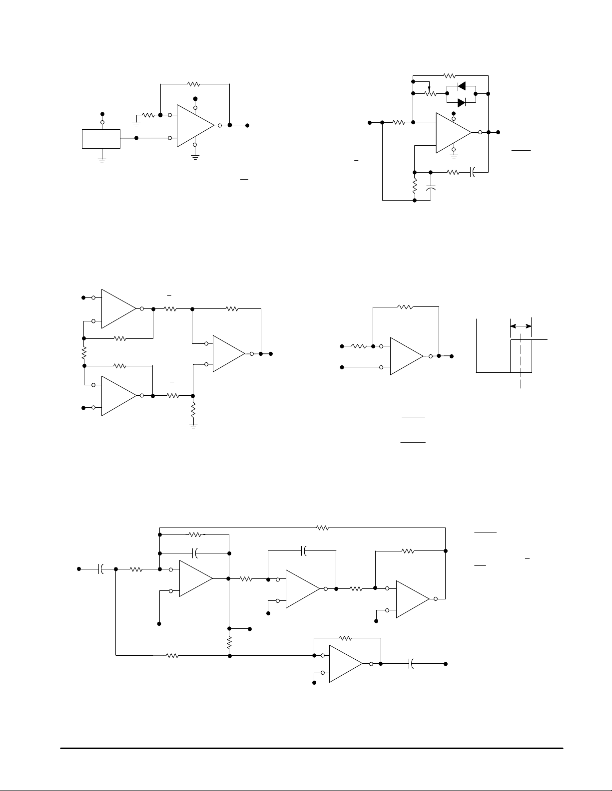
Figure 11. Bi–Quad Filter
ref
C
–
1/2
LM358
+
V
R
V
Bandpass
Output
R1
ref
R
R3
–
1/2
LM358
+
100 k
Where:
fo =
100 k
R1 = QR
R2 =
For:
R3 = TN
C1 = 10 C
f
o
Q
T
BP
T
N
–
1/2
LM358
+
V
ref
C1
Notch Output
TBP = Center Frequency Gain
TN = Passband Notch Gain
1
π
RC
2
R1
T
BP
R2
= 1.0 kHz
= 10
= 1
= 1
V
ref
R
= 160 k
= 0.001 µF
C
= 1.6 M
R1
= 1.6 M
R2
= 1.6 M
R3
1
=V
CC
2
Ω
Ω
Ω
Ω
5

LM358, LM258, LM2904, LM2904V
Figure 12. Function Generator Figure 13. Multiple Feedback Bandpass Filter
V
=V
ref
V
ref
1
CC
2
Triangle Wave
+
1/2
LM358
–
C
f =
Output
R1 + R
4 CRf R1
R2
300 k
R3
75 k
R1
100 k
V
ref
R
f
R3 =
R2 R1
R2 + R1
C
if,
+
1/2
LM358
–
Square
Wave
Output
V
R1
in
For less than 10% error from operational amplifier.
Where fo and BW are expressed in Hz.
If source impedance varies, filter may be preceded with voltage
follower buffer to stabilize filter parameters.
C
C
R2
Given: fo = center frequency
A(fo) = gain at center frequency
Choose value fo, C
R1 =
R2 =
4Q2 R1 –R3
Q
π
fo C
R3
2 A(fo)
R1 R3
Then: R3 =
R3
V
ref
V
–
1/2
LM358
+
CC
CO
CO = 10 C
1
V
=V
ref
2
Qo f
o
< 0.1
BW
V
CC
O
6
MOTOROLA ANALOG IC DEVICE DATA

NOTE 2
–T–
SEATING
PLANE
H
LM358, LM258, LM2904, LM2904V
OUTLINE DIMENSIONS
58
–B–
14
F
–A–
C
N
D
G
0.13 (0.005) B
K
M
T
N SUFFIX
PLASTIC PACKAGE
CASE 626–05
ISSUE K
L
J
M
M
A
M
NOTES:
1. DIMENSION L TO CENTER OF LEAD WHEN
FORMED PARALLEL.
2. PACKAGE CONTOUR OPTIONAL (ROUND OR
SQUARE CORNERS).
3. DIMENSIONING AND TOLERANCING PER ANSI
Y14.5M, 1982.
DIM MIN MAX MIN MAX
A 9.40 10.16 0.370 0.400
B 6.10 6.60 0.240 0.260
C 3.94 4.45 0.155 0.175
D 0.38 0.51 0.015 0.020
F 1.02 1.78 0.040 0.070
G 2.54 BSC 0.100 BSC
H 0.76 1.27 0.030 0.050
J 0.20 0.30 0.008 0.012
K 2.92 3.43 0.115 0.135
L 7.62 BSC 0.300 BSC
M ––– 10 ––– 10
N 0.76 1.01 0.030 0.040
INCHESMILLIMETERS
__
C
A
E
B
A1
D SUFFIX
PLASTIC PACKAGE
CASE 751–05
(SO–8)
ISSUE R
D
58
0.25MB
1
H
4
e
M
h
X 45
_
q
C
A
SEATING
PLANE
0.10
L
B
SS
A0.25MCB
NOTES:
1. DIMENSIONING AND TOLERANCING PER ASME
Y14.5M, 1994.
2. DIMENSIONS ARE IN MILLIMETERS.
3. DIMENSION D AND E DO NOT INCLUDE MOLD
PROTRUSION.
4. MAXIMUM MOLD PROTRUSION 0.15 PER SIDE.
5. DIMENSION B DOES NOT INCLUDE MOLD
PROTRUSION. ALLOWABLE DAMBAR
PROTRUSION SHALL BE 0.127 TOTAL IN EXCESS
OF THE B DIMENSION AT MAXIMUM MATERIAL
CONDITION.
MILLIMETERS
DIM MIN MAX
A 1.35 1.75
A1 0.10 0.25
B 0.35 0.49
C 0.18 0.25
D 4.80 5.00
E
3.80 4.00
1.27 BSCe
H 5.80 6.20
h
0.25 0.50
L 0.40 1.25
0 7
q
__
MOTOROLA ANALOG IC DEVICE DATA
7

LM358, LM258, LM2904, LM2904V
Motorola reserves the right to make changes without further notice to any products herein. Motorola makes no warranty , representation or guarantee regarding
the suitability of its products for any particular purpose, nor does Motorola assume any liability arising out of the application or use of any product or circuit, and
specifically disclaims any and all liability, including without limitation consequential or incidental damages. “T ypical” parameters which may be provided in Motorola
data sheets and/or specifications can and do vary in different applications and actual performance may vary over time. All operating parameters, including “Typicals”
must be validated for each customer application by customer’s technical experts. Motorola does not convey any license under its patent rights nor the rights of
others. Motorola products are not designed, intended, or authorized for use as components in systems intended for surgical implant into the body, or other
applications intended to support or sustain life, or for any other application in which the failure of the Motorola product could create a situation where personal injury
or death may occur. Should Buyer purchase or use Motorola products for any such unintended or unauthorized application, Buyer shall indemnify and hold Motorola
and its officers, employees, subsidiaries, affiliates, and distributors harmless against all claims, costs, damages, and expenses, and reasonable attorney fees
arising out of, directly or indirectly, any claim of personal injury or death associated with such unintended or unauthorized use, even if such claim alleges that
Motorola was negligent regarding the design or manufacture of the part. Motorola and are registered trademarks of Motorola, Inc. Motorola, Inc. is an Equal
Opportunity/Affirmative Action Employer.
How to reach us:
USA/EUROPE /Locations Not Listed: Motorola Literature Distribution; JAPAN: Nippon Motorola Ltd.; Tatsumi–SPD–JLDC, 6F Seibu–Butsuryu–Center,
P.O. Box 20912; Phoenix, Arizona 85036. 1–800–441–2447 or 602–303–5454 3–14–2 Tatsumi Koto–Ku, Tokyo 135, Japan. 03–81–3521–8315
MFAX: RMF AX0@email.sps.mot.com – TOUCHT ONE 602–244–6609 ASIA/PACIFIC: Motorola Semiconductors H.K. Ltd.; 8B Tai Ping Industrial Park,
INTERNET: http://Design–NET.com 51 Ting Kok Road, Tai Po, N.T., Hong Kong. 852–26629298
8
◊
MOTOROLA ANALOG IC DEVICE DATA
LM358/D
*LM358/D*
 Loading...