

Page 1

MOTOKRZR K3 – Theory of operation - v.1.0. – 2006.12.10
MOTOKRZR K3
Theory of operation
1. Overview
Motorola MOTOKRZR K3 phone delivers 3G features in a thin and narrow clam KRZR form factor. It is
a dual-mode phone, tri-band GSM plus W-CDMA 2100 for the European market. It is based on the
Freescale Argon LV and RF Colorado2 platform.
As a 3G product, the MOTOKRZR K3 complies with all key specifications as defined by the 3GPP.
Key Points and Features
• Form Factor: Thin Clam
• Finish: Premium CMF
• Color: Dark Pearl Grey, Stone Grey
• Dimensions: 103.2 x 42.3 x 16.3mm / Approx 63cc
• Bands/Modes: WCDMA 2100 (HSDPA DL 3.6Mbps), GSM/GPRS class 12/EDGE class 12
triband: 900/1800/1900
• Antenna: internal – main (GSM TX/RX), secondary (WCDMA RX), Bluetooth
• Imagers - external: 2MP Camera – internal (for video telephony): VGA
• Display – internal: 2.0” 240x320 QVGA 262K color – external (for CLI): 1.3” 120 x 160 262K
TFT
• Memory: 64M On-Board plus removable Micro SD slot
• Bluetooth: Stereo (A2DP/AVRCP)
• Messaging: MMS, EMS 5.0, IM Wireless Village, Email (POP3, SMTP, IMAP4)
• Video: MPEG4, h.263 Capture / playback
• Audio: MIDI,MP3, WMA, AAC / AAC+ , Enhanced AAC+, WMA
• Connectivity: Mini USB 2.0 FS, MotoSync, BT Class 2
• Speakers: Independent Name & Digit Dialing
• Battery: BT50 High Capacity (min: 910mAh, typ: 950 mAh)
Level 3 Page 1
Page 2
MOTOKRZR K3 – Theory of operation - v.1.0. – 2006.12.10
2. Overall block diagram
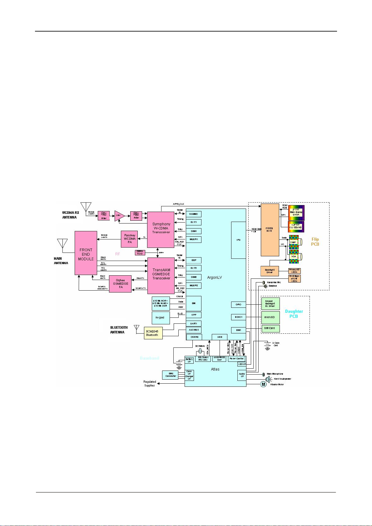
The overall block diagram is shown in Figure 1
The phone is equipped with three antennas. The first one (MAIN low-profile FICA antenna) is a
tri-band antenna used for both TX and RX on GSM bands, along with WCDMA TX. The connection
to the proper TX/RX line-up is switched by the front-end module (FEM).
The second antenna is connected to the only WCDMA RX line-up, thus providing a way to monitor
the WCDMA downlink signal, independently of the band and the technology that the phone is
transmitting and camped on. In particular, it is not necessary to use downlink compressed mode for
3G-2G hand-over, while in WCDMA call and monitoring GSM cell by the main antenna. However,
compressed mode must be used for uplink in the same scenario – since the WCDMA TX signal is
switched by the FEM along with the GSM RX ones.
The third antenna is used by the only Bluetooth IC, for both TX and RX
Figure 1. Overall block diagram
Level 3 Page 2
Page 3
MOTOKRZR K3 – Theory of operation - v.1.0. – 2006.12.10
3. RF Section
3.1. Front-end module
The Front End Module integrates two GaAs switches, a diplexer, and a 3-line control decoder in a
low profile plastic mold package. A simplified block diagram is shown in Figure 2.
The module provides band selection and filtering between the antenna and the transceiver circuitry
for Colorado II chipset-based phones. This includes GSM850, GSM900 and WB850 band V (which
includes Japanese band VI) receive and transmit bands on the low pass side of the diplexer, and
GSM1800, GSM1900, WB1900 (band II) receive and transmit bands, and WB2100 (band I) transmit
band on the high pass side. This phone uses only the GSM900, DCS1800, PCS1900 and
WCDMA2100 paths.
Figure 2. Front-end module (FEM) simplified block diagram
As mentioned in the previous section, the design of this module is assuming a separate antenna
dedicated to the WCDMA2100 receiver. This antenna should have at least 10 dB isolation from the
main antenna in the 2110-2170 MHz band.
3.2. RF WCDMA Receiver
3.2.1. LNA (U300)
WCDMA receive signals from the secondary antenna are fed into a ceramic 3-pole pre-select band
pass filter (FL001) through an antenna matching network and RF connector (M002). If M002 is used,
all WCDMA signals are fed into M001. Also, the internal antenna path will be in an open state when
M001 is used.
From the band-pass filter, the W2100 Rx signal is fed into the 2100 MHz band Low Noise Amplifier
(U300) through a second Rx matching network.
The LNA is controlled by Symphony through two enable lines. Gain line is used to put LNA into either
Level 3 Page 3
Page 4
MOTOKRZR K3 – Theory of operation - v.1.0. – 2006.12.10
high gain or low gain mode, depending on the input power level. The LNAs turn off at antenna input
level threshold around -70 dBm and turns on at input level threshold around -68 dBm.
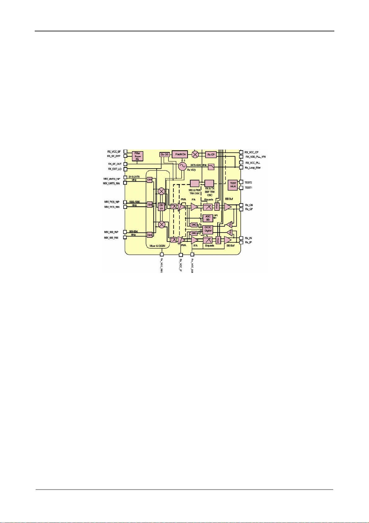
3.2.2. Symphony Rx (U100)
Symphony (U100) is a programmable mixed-signal quadband exciter (Tx) and receiver back-end
(Rx) for a UMTS W-CDMA cellular radio (UE) operating in FDD mode. The functional interface of this
part is RF at the carrier frequency and digital baseband. The four bands supported are UMTS (Band
I), North American PCS (Band II), North American 800 (Band V), and Japan 800 (Band VI). Only
Band I is used for this phone.
Figure 3 Symphony (Rx)
The frequency generation within the part supports variable duplex frequency spacing (Rx/Tx) per
3GPP requirements though the intention at this time is to use the part in fixed duplex mode. Because
of this requirement, the Rx and Tx have separate VCO’s and PLL’s, and their operation is
independent of the other. Loop filters are internal to the module.
The SPI (serial programming interface) is used to setup the part for operation and is programmed by
the baseband processor. The SPI supports read and write operations to/from the internal
programmable registers. In addition to static operational modes defined by some of the register
values, the part also includes “sequence managers” that utilize a pre-programmed sequence of
instructions to dynamically enable, control, and disable the transceiver. The sequence managers
are triggered by layer 1 timed control signals from the baseband processor.
The receiver architecture is a direct conversion receiver (DCR). The inputs drive three sets of
differential quadrature mixers, one for each frequency band. Preselection filters, LNA’s, and
interstage filters must be provided externally to the inputs. The mixer inputs are internally matched to
pre-defined interstage filter output impedances.
The mixer zero-IF outputs are low pass filtered and amplified internally with a variable gain amplifier,
also known as the post-mixer amplifier (PMA). The dynamic range of the PMA is driven by the AGC
system requirements. Finally, the I/Q signals are digitized, digitally filtered, and output in a serial
fashion to the DSP demodulator in the baseband processor.
This particular module is a Multi-Chip Module (MCM) integrated on an organic High Density
Level 3 Page 4
Page 5
MOTOKRZR K3 – Theory of operation - v.1.0. – 2006.12.10
Interconnect (HDI) substrate. The module contains two IC’s named internally as “Melody”
(RF/baseband interface IC) and “Viper” (RFIC). Supporting discrete components are placed inside
the module such as impedance matching networks, PLL loop filters, and supply bypass capacitors.
Melody is paired with ArgonLV (U1000), which is the baseband processor. ArgonLV includes the
DSP core known as “WAMMO”.
3.3. RF WCDMA Transmitter
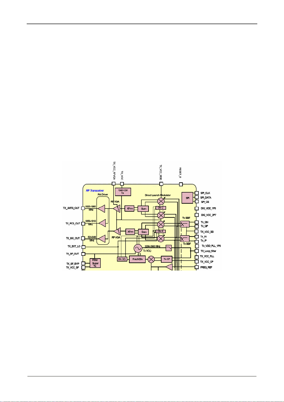
3.3.1. Symphony Tx (U100)
The transmitter architecture is direct launch. The inputs are serial digital baseband I/Q from the DSP
modulator in ArgonLV. They are digitally filtered and then converted to baseband analog signals.
After filtering, the I/Q signals are quadrature modulated and upconverted directly to the carrier
frequency. The RF signal is input to a variable gain amplifier (VGA) that is controlled by the AOC
feedback system for precise power control.
Finally, the RF is routed to a set of three PA driver stages, one for each frequency band, that serves
as the module’s output. Provided externally to this part are pre-PA filtering, PA amplification, power
detection, and final Tx filtering.
Figure 4 Symphony (Tx)
3.3.2. WCDMA PA (U400)
The PASSKEY-5W PA (U400) is a 50 ohm, single-band, single-mode, WCDMA PA modules
intended for 3G radio applications. The module integrates an inter-stage filter, power amplifier,
coupler, power detector. It has Tx band-pass filter internal to the module.
The 5W module includes a Tx band-pass filter at the input and output, as shown in the module block
diagram in Figure 5.
A Motorola proprietary high power / low power efficiency enhancement load (EE Ld) switch is
included in the output match. For the EE Ld switch, VMODE voltage level changes the output load
Level 3 Page 5
Page 6
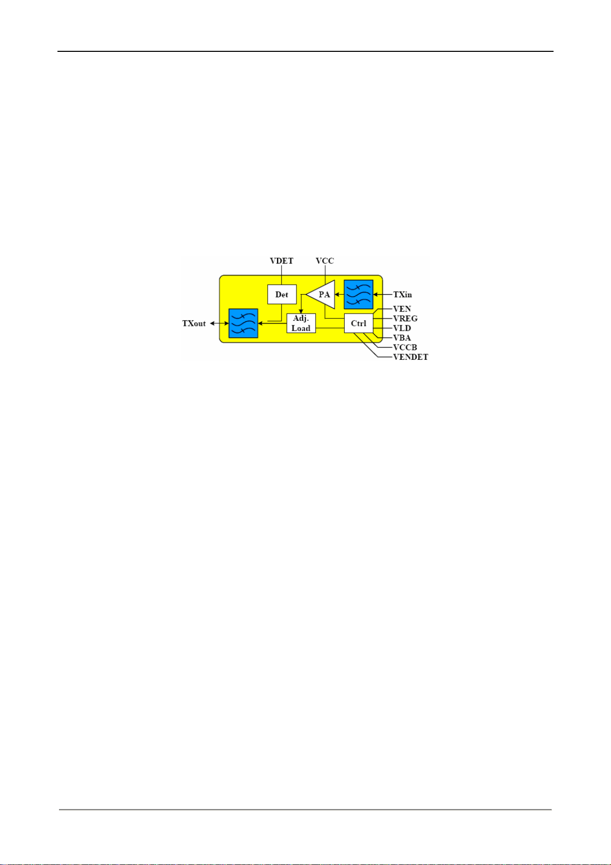
MOTOKRZR K3 – Theory of operation - v.1.0. – 2006.12.10
for optimum efficiency from low power to high power out. A bias line (Vba) is available for band/mode
optimization for ACLR and current.
The PA has an internal RF detector which is used for feedback to the AOC system.
The PA can be set in two modes, the High Power Mode (HPM) and the Low Power Mode (LPM). The
modes are selected by setting WB_PA_VLD (Vmod) line. When VLD is set high (2.4V), the PA is in
LPM. When VLD is set low (0V), the PA is in HPM. In LPM, the gain of the PA is variable. The PA
gain can be varied by applying different PA biases on the WB_PA_VBIAS (VBA) line. The range for
LPM is from 16dBm to below -50dBm. In HPM the gain of the PA is the highest, about 20 to 23 dB.
HPM is any power above 16dBm to 23 dBm at the antenna port. The PA bias, VBA is set to about
2.2V.
Figure 5. Passkey 5W PA block diagram
The WCDMA TX lineup can also be operated in a Open Loop or Closed Loop Mode. The Open Loop
mode is generally from below -50 to +3dBm, below the operating range of the RF detector. The Tx
power is set by calibration tables. The AOC system calculates the required TX index for the required
power level and applies any channel LPM correction. Since the detector feedback is not used, the
AOC system is not aware of the actual transmitted power.
The Closed Loop Mode is power levels above 3dBm, within the range of the RF detector. The Tx
power is dynamically adjusted based on RF detect feedback. The detector within the PA is used to
provide feedback to Symphony (AOC system) about the current output power level from the PA.
3.4. EGPRS Transceiver
3.4.1. Introduction
This phone is using an highly integrated EGPRS transceiver providing bits to antenna capability
through the combination of the TransAAM transceiver module with the Orphee PA module. Figure 6
shows the major subsystems integrated into the TransAAM / Orphee modules.
The transceiver works over the GSM850 (not used on this phone), EGSM900, DCS1800, and
PCS1900 transmit and receive frequency bands. It includes a VLIF/DCR receive architecture with
integrated LNAs and a polar modulation transmit architecture with direct modulation of the VCO by a
fractional-N synthesizer. Both the RX and TX VCOs are fully integrated. The polar architecture
allows for a filter-free transmit lineup.
An on-chip transmit/receiver sequencer generates appropriate timing events for the transmitter
calibration and the EDGE/GMSK transmit/receive burst, therefore, limiting the RF hardware
dependency of the L1 engine software to an absolute minimum. The DigRF standard defines the
Level 3 Page 6
Page 7
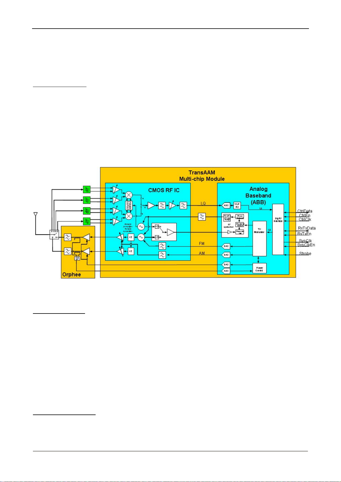
MOTOKRZR K3 – Theory of operation - v.1.0. – 2006.12.10
digital interface between the TransAAM and the baseband processor IC.
3.4.2. Trans-AAM (U500)
Rx Analog Section
providing functionality for GSM850, EGSM900, DCS1800 and PCS1900 frequency bands. The
LNAs are differential and provide 30 dB of dynamic range as digital steps, eliminating the need for
RX AGC gain.
The quadrature mixer down-converts the RF signal to baseband. Passive differential and common
mode filtering at the mixer output limits out of band signals in the active stages of the baseband
section and results in an IP2 of 55 dBm (including processor gain). The I and Q analog baseband
signals are passed through low pass anti-aliasing filters and dc offset correction circuits before being
processed by the analog-to-digital converters.
-The RX architecture is digital VLIF/DCR. There are four separate LNAs
Figure 6. EGPRS transceiver - TransAAM and Orphee connections
TX Analog Section
VCO. The module can transmit in GMSK (phase modulation) or 8PSK (phase and amplitude
modulation) mode.
In GMSK mode, the dual port TX VCO is phase modulated by the dual port synthesizer and the
signal is fed to the PA input at a fixed level.
In 8PSK mode, the additional amplitude modulation is performed via a commuting switch mixer. The
mixer core drives a resistive digital step attenuator, which provides 0 to 45 dB of dynamic range in 3
dB steps, allowing the required full dynamic range to cover all EDGE power steps with only 20 dB of
dynamic range from the modulator. Two DACs provide signals to the modulator. One DAC is
dedicated to the amplitude component of the 8PSK wave form and the other to driving the VCO high
port input.
Frequency Generation
resonators with 32 states of digital course tuning. The frequency synthesizer is a 24-bit, 3rd order
fractional N synthesizer with digital AFC and a lock time of less than 80 µs. A 26 MHz crystal
oscillator provides a stable frequency reference. The VCO output signal runs through a
- The TX architecture is a polar modulator with direct digital modulation of the
- Both the RX and TX VCO run at 3296 to 3820 MHz and have integrated
Level 3 Page 7
Page 8

MOTOKRZR K3 – Theory of operation - v.1.0. – 2006.12.10
divide-by-two for operation in the DCS/PCS bands and a divide-by-four for operation in the 850GSM
and EGSM bands. Operation at 2 or 4 times the LO frequency provides good immunity to
re-modulation. VCO feedback to the “divide-by-N” is through a fixed divide-by-3. The output of the
divide-by-N is compared to a 26 MHz reference in the phase comparator and error output is passed
through the loop filter before being applied to the VCO. The corrected clock module is a 22-bit digital
phase-locked loop used to provide an accurate 26 MHz reference, synchronized to the GSM system,
when the system is operated from an uncorrected crystal. The 26 MHz reference crystal oscillator
provides a stable frequency reference for the major functions in the radio system. The crystal output
can also be routed to two auxiliary reference pins to provide a reference clock for RF accessories
such as Bluetooth, GPS, and WLAN.
Digital Core
• Receive coprocessor (RxCPROC). The digital portion of the RX signal processing chain,
• DigRF. Interface to the baseband IC using the DigRF standard. The DigRF standard
• Transmit module (TXM). The EDGE/GMSK digital transmit module (TXM) contains two
• Transmit/receiver timing sequencer (TRXQ). This module generates appropriate timing
- The digital core of the MMM6000 consists of four major functional blocks:
consisting of decimation filters, a digital LO generator, complex mixers, adjustable channel
filters, and a DC adapt module. The initial conversion is done by the sigma-delta modulator
and the results are passed into the RxCPROC. Processed signals are sent serially to the
baseband IC through the DigRF interface port.
specifies the logical electrical, and timing details of the RF/Baseband interface. This
standard can be found at: www.digrf.com
modulation schemes (GMSK and 8PSK) and supports amplitude/phase (polar pair), or
amplitude/frequency modulation.
events for the transmitter calibration and the EDGE/GMSK transmit/receive burst, therefore,
limiting the RF hardware dependency of the L1 engine software to the absolute minimum.
.
3.4.3. Orphee PA (U800)
Orphee is a quad band Class 12 EGPRS front end module. Along with the power amplifier, Orphee
contains the harmonic filters, direction coupler, power detector, antenna switch and a power control
circuit. The block diagram of Orphee is shown below in Figure 7.
Orphee uses a separate RF lineup for lowband and highband as is common with most quad-band
designs. The first two stages are implemented in SiGe HBT while the third stage is a InGaP HBT.
Separate couplers are used for the paths to avoid issues with combining and daisy chaining of
couplers seen in the past.
Log detector
The log detector provides a higher sensitivity and higher dynamic range detector. The high
sensitivity enables loose coupling and low insertion loss in the output network, as well as the
increased dynamic range allows closed loop operation at very low levels.
Power Control
Orphee supports multiple modes of power control operation. For operation with TransAAM, it uses
bias control mode for GMSK modulation and input power control mode for 8PSK modulation. This
configuration allows the combined system to operate without SAW filters in the TX path.
For bias control mode, the power control system is a double loop system consisting of the inner
Level 3 Page 8
Page 9

MOTOKRZR K3 – Theory of operation - v.1.0. – 2006.12.10
analog loop on Orphee and the digital loop on TransAAM. In this mode of operation, the RF input
signal to the PA is a constant value. In the analog loop, the Vramp signal applied from TransAAM is
lowpass filtered and compared to the Vdetect signal processed through the Vdetect buffer. The
integral controller generates an output based on the difference between the signals, Vapc. This is
then routed through the PA Bias Selector to the PA Bias Controller where it is used to vary PA bias
and therefore power output. This changes Vdetect and the analog loop drives the value of buffered
Vdetect to be equal to filtered Vramp. The digital loop operates outside of the analog loop. It receives
a Vdetect value which is digitized, compared to a reference value and an error signal generated. The
digital error signal is sent to a DAC where it becomes the Vramp signal sent to Orphee. The ramp
generation for power up and power down is performed in the digital section on TransAAM.
Figure 7. Orphee PA block diagram
For input power control mode with TransAAM, the analog loop is disconnected. As the name implies,
power output is controlled by varying the input power from TransAAM. As such, Orphee will be
configured to a fixed gain configuration. The Vramp signal is a fixed dc value and the PA bias
selector routes this signal to the PA bias controller where is sets the operating point. TransAAM
varies input power and monitors the Vdetect signal to perform power control.
Level 3 Page 9
Page 10

MOTOKRZR K3 – Theory of operation - v.1.0. – 2006.12.10
4. Baseband Section
4.1. ArgonLV
4.1.1. Argon LV processor
ArgonLV is the main processor used for all system and user applications.
As shown in Figure 8, the Argon IC integrates the following three main cores:
• Microcontroller Unit (MCU): 400MHz ARM11 used for operating system, user applications and
call control.
• Digital Signal Processor (DSP): 208MHz Motorola StarCore used for call and audio data
processing.
• Smart DMA (SDMA): 100MHz Direct Memory Access Controller used to assist communications
between the MCU and DSP.
ArgonLV contains built in interfaces for all phone peripherals, such as MMC/SD Card, IrDA, USIM,
RS-232 Serial (Bluetooth), USB (EMU) and a Dedicated Smart Display interface for communicating
with graphics processor in the flip.
Figure 8. Argon LV block diagram
Level 3 Page 10
Page 11

MOTOKRZR K3 – Theory of operation - v.1.0. – 2006.12.10
4.1.2. Memory
Three types of memory are used with ArgonLV
• NOR Flash: 512Mbit used for code storage. This is programmed at the factory flash and CFC
stations. Code is executed from these parts directly.
• NAND Flash: 512Mbit used for the phone filesystem. This space is intended for user storage of
songs, videos, etc. This space will be formatted at the factory flash station.
• SDRAM: 512Mbit of DDR memory.
The NOR Flash and DDR memory share address lines and the NOR Flash and the NAND Flash
share data lines.
4.1.3. ArgonLV PoP
U1000 is ArgonLV Package on Package (PoP), which is packaged with memory interface pinned out
on the top of the package. The memory is packaged into a single 15x15 MCP package to be placed
on top of ArgonLV PoP package. The parts come in discretely and are placed and reflowed on the
production line.
ArgonLV PoP provides significant reduction in board space by combining discrete memories into
single MCP and stacking on top of the processor.
Figure 9. ArgonLV/Memory PoP cross section
4.2. Atlas IC (U3000)
4.2.1. Overview
The Atlas IC is an ASIC intended for use in Argon/Atlas platform mobile phones. It integrates several
voltage regulators of both linear and switching types designed for use in the power scheme, audio
codecs and amplifiers, serial and USB transceivers, back- and service- light LED controllers and
digital interfaces to one or two controlling processors.
A simplified block diagram is shown in Figure 10.
4.2.2. Atlas Power supply architecture
The main battery voltage range is from 3.1V to 4.2V. Atlas regulates the main battery voltage to
Level 3 Page 11
Page 12

MOTOKRZR K3 – Theory of operation - v.1.0. – 2006.12.10
power the ICs in the phone. Some typical voltages are as follows:
• 1.5V: Argon and Graphics Processor cores
• 1.8V: Memory cores, many I/O supplies
• 2.775V: Some peripheral cores, I/O supplies
• 3.3V: USB transceiver, Argon eFusing
• 5.5V: Used to generate 3.3V
Some voltages are provided by more than one regulator. There are three switching regulators (1.5V,
1.8V, and 5.5V) and many linear regulators. Atlas also handles battery charging.
Figure 10 Atlas simplified block diagram
4.2.3. Atlas Audio
Atlas also provides the audio functions for the phone. Atlas has the analog connections to all the
transducers such as Microphone, Earpiece speaker, Loudspeaker and EMU headset microphone
and speakers. Simplified block diagrams for all Atlas audio functions are shown in the following, from
Figure 11 to Figure 15.
Atlas also handles the digital to analog conversion of all audio, in both directions. There are two
digital paths. One handles bidirectional AMR audio, which occurs during phone calls. The ASAP
interface carries this traffic between Argon, Atlas and Bluetooth. The second (MMSAP) handles
multimedia audio. This path is output only but can play both stereo and mono audio. Usually this is
used by the MP3 and movie players.
Level 3 Page 12
Page 13

MOTOKRZR K3 – Theory of operation - v.1.0. – 2006.12.10
Figure 11 Audio Tx Path Block Diagram
Figure 12 Audio Rx Path Block Diagram
Figure 13 Handset/Internal Mic Circuit
Figure 14 Earpiece/Handset Speaker Circuit
Level 3 Page 13
Page 14

MOTOKRZR K3 – Theory of operation - v.1.0. – 2006.12.10
Figure 15 Loudspeaker Circuit
4.2.4. Charging Control
This phone is using a dual path charger mode. Its architecture is shown in Figure 16.
Figure 16 Dual Path Charging Architecture
Figure 17 shows the simplified charging block diagram. M1 and M2 are on the Two Way Power line.
M3 is from a bttery to B+. M4 is charger to B+. The same Figure 17 shows the truth table for the
charge control.
Figure 17 Charging path block diagram and truth table for charge control
Level 3 Page 14
Page 15

MOTOKRZR K3 – Theory of operation - v.1.0. – 2006.12.10
4.3. Bluetooth
4.3.1. Overview
This phone uses Broadcomm BCM2045 (U5600) Single Chip solution for Bluetooth connectivity
The BCM2045 is compliant to Bluetooth Core Specification version 1.2 compliant, and designed for
use in standard HCI UART or HCI USB applications. The combination of the BBC, PTU and the
ROM based UPU provide a complete lower layer Bluetooth protocol stack including the link
controller (LC), link manager (LM), and HCI interface.
Figure 18 shows the interconnect of all the major physical blocks in the BCM2045 and their
associated external interfaces.
Figure 18. Broadcomm BCM2045 Bluetooth IC block diagram
4.3.2. Integrated Radio Transceiver
The BCM2045 features a fully integrated zero IF transmitter. The baseband transmit data is digitally
GFSK modulated in the modem block and up-converted to the 2.4-GHz ISM band in the transmitter
path. The transmitter path consists of signal filtering, I/Q up-conversion, output power amplifier (PA),
and RF filtering. It also incorporates new modulation schemes Π/4-DQPSK for 2 MBps and 8-DPSK
for 3 MBps to support enhanced data rate.
The digital modulator performs the data modulation and filtering required for the GFSK, Π/4DQPSK,
and 8-DPSK signal. The digital demodulator and bit synchronizer takes the low IF received signal
Level 3 Page 15
Page 16

MOTOKRZR K3 – Theory of operation - v.1.0. – 2006.12.10
and performs an optimal frequency tracking and bit synchronization algorithm.
The fully integrated PA provides a maximum output signal level of +4 dBm using a highly linearized,
temperature compensated design.
The receiver path uses a low IF scheme to down-convert the received signal for demodulation in the
digital demodulator and bit synchronizer. The digital demodulator and bit synchronizer takes the low
IF received signal and performs an optimal frequency tracking and bit synchronization algorithm.
The radio portion of the BCM2045 provides an RSSI signal to the baseband so that the controller
can take part in a Bluetooth power-controlled link by providing a metric of its own receiver signal
strength to determine whether the transmitter should increase or decrease its output power.
Local Oscillator (LO) generation provides fast frequency hopping (1600 hops/second) across the 79
maximum available channels.
4.3.3. Bluetooth Baseband Core (BBC)
The Bluetooth Baseband Core (BBC) implements all of the time critical functions required for high
performance Bluetooth operation. The BBC manages the buffering, segmentation, and routing of
data for all connections. It also buffers data that passes through it, handles data flow control,
schedules SCO/ACL TX/RX transactions, monitors Bluetooth slot usage, optimally segments and
packages data into baseband packets, manages connection status indicators, and composes and
decodes HCI packets. In addition to these functions, it independently handles HCI event types, and
HCI command types.
The following transmit and receive functions are also implemented in the BBC hardware to increase
reliability and security of the Tx/Rx data before sending over the air
• Symbol timing recovery, data de-framing, forward error correction (FEC), header error
control (HEC), cyclic redundancy check (CRC), data decryption, and data de-whitening in the
receiver.
• Data framing, FEC generation, HEC generation, CRC generation, key generation, data
encryption, and data whitening in the transmitter.
4.3.4. Microprocessor Unit (µPU)
The microprocessor unit (µPU) runs software from the link control (LC) layer, up to the host
controller interface (HCI). The microprocessor is based on ARM7TDMIS 32-bit RISC processor with
embedded ICE-RT debug and JTAG interface units.
The µPU also consists of the peripheral input/output, 192 KB of ROM memory for program storage
and boot ROM, 40 KB of RAM for data scratchpad and patch RAM code. At power-up, the lower
layer protocol stack is executed from the internal ROM memory.
4.3.5. Peripheral Transport Unit (PTU) - UART
The UART physical interface is a standard, 4-wire interface (RX,TX, RTS, CTS) with adjustable
baud rates from 9600 bps to 3.0 Mbps. The interface features an automatic baud rate detection
capability that returns a baud rate selection.
Level 3 Page 16
Page 17

MOTOKRZR K3 – Theory of operation - v.1.0. – 2006.12.10
The BCM2045 has a 480-byte receive FIFO and a 480-byte transmit FIFO to support enhanced data
rate. The interface supports the Bluetooth 1.2 UART HCI specification.
4.3.6. Frequency References
The BCM2045 uses two different frequency references for normal and low-power operational modes.
An external crystal or external frequency reference driven by a temperature compensated crystal
oscillator (TCXO) signal is used for the generation of all radio frequencies and normal operation
clocking.
The external 32.768 kHz is used for low power mode timing.
4.4. USIM Interface
For 3G, the traditional SIM card is being called the USIM (Universal Subscriber Identity Module). The
USIM will be contained on a UICC (Universal Integrated Circuit Card), which will be a removable
module. The USIM shall contain an identity that unambiguously identifies a subscriber. The USIM
will also provide storage for subscription and subscriber-related information. It will need to be
resident in the radio for a call to be initiated. If it is not present, the user will be informed that the
USIM is missing by a message on the display. If the USIM is removed during a call, the call will be
terminated. Access to 3G services without a UICC containing a valid USIM will be available only for
emergency calls.
Figure 19. USIM Interface Block Diagram
The SIM Interface Module (SIM) in Argon LV will provide support for T=1 type SIM cards. Of the two
ports available in the ArgonLV SIM, only Port 0 will be used.
According to the 3GPP specifications, USIM support should be available over at least the following
ranges: 3.0V ±10% and 1.8V ±10%. In specifications such as TS 31.101, the 1.8V supply voltage
range is called “Class B” while the 3V supply voltage range is called “Class C.” Both the 1.8V and 3V
ranges will be supported by M702iS. USIM cards will contain an identification coded into bits 5-7 of
their status information that will identify them as the appropriate technology USIM.
USIM communicates with M702iS via the SIM (Smartcard Interface Module) of the Argon LV.
According to ISO 7816, GSM 11.12, and GSM 11.18, the clock going to the USIM should be
between 3 to 4 MHz. The exact frequency will be 3.25 MHz. The SIM module in Argon contains a
block designed specifically for generating the clocks used internal to the SIM module, and the clocks
Level 3 Page 17
Page 18

MOTOKRZR K3 – Theory of operation - v.1.0. – 2006.12.10
provided to the SIM cards.
The USIM presence detect line will be active low. If a USIM is not present, the display will show a
USIM insertion error. If the battery is detected, Argon will try to initiate communications with the
USIM. If there is no response, an “Insert USIM” error will result.
4.5. MicroSD memory card interface
The Argon based platforms will interface with a type of NAND flash memory card known as microSD.
This type of card is capable of Multimedia Card (MMC), Secure Digital (SD) card, and SPI modes.
The microSD card contains a high-density flash memory as well as a controller that gives the user
the ability to store personal files and use them in low-bandwidth applications.
Figure 20. MicroSD interface block diagram
For Argon based platforms, the Secure Digital Host Controller (SDHC) module will provide the
necessary signals for communication with microSD cards. Because of the microSD connector’s
small size, the larger MMC and SD cards will not be supported. However, a microSD to SD “adaptor
card” will be available that will allow users to access files with their PC using a USB-based SD card
reader.
The VMMC_2.9V supply will provide power to the Vdd pin on the card. The maximum clock
frequency for SD devices is 25 MHz. The SDHC module of Argon supports a maximum operating
frequency of 25MHz and its base clock is the MCU peripheral clock divided by 5. The final clock rate
will be determined by the value of the CLK_RATE register in Argon.
4.6. EMU Interface
4.6.1. Overview
The EMU (Enhanced Mini-USB) bus is an interface that incorporates support for the CEA-936A
carkit specification, charging from a variety of sources, USB connectivity, as well as support for
phone-powered accessories.
The EMU Accessory connector is a standard mini USB connector with a total of 5 pins and is directly
connected to the Atlas IC. Atlas provides audio support through EMU for accessories. In addition to
Level 3 Page 18
Page 19

MOTOKRZR K3 – Theory of operation - v.1.0. – 2006.12.10
the signaling modes, Atlas integrates all necessary logic to take on the task of controlling the dual
path charging lineup, as previously described
When a device is connected to the EMU bus, Atlas will identify the device based on the states of the
VBUS, D+, D-, and ID pins. Atlas utilizes three different detectors to determine which type of device
is connected. A change in status on any of the following 3 detectors will generate an interrupt and the
status can be read from the appropriate status register.
• Vbus Detector - Three comparators are used to detect the voltage level on VBUS. USBDET4V4
detects a valid VBUS while USBDET2V0 and USBDET0V8 support the USB OTG session
request protocol. Each have a sense bit (USB4V4S, USB0V8S, and USB2V0S) located in the
interrupt sense register. These sense bits are 1 when the VBUS level is above the detected
threshold. On any rising or falling edge of the comparator outputs, a USBI interrupt is generated.
VBUS can be connected to the charger input pin for joint charging and USB signaling.
• SE1 Detector - To distinguish different phone accessories, an SE1 detector checks to see if the
signal on D+ and D- are above a positive threshold. If so, the SE1S bit will be set high. Any
change in SE1S generates an SE1I interrupt.
• ID Detector - Used primarily to distinguish between mini-A and mini-B style plugs being inserted
into the mini-AB receptacle. However, the ID pin supports two additional modes outside of USB
standards: factory test mode and non USB accessory mode. The state of the ID detector can be
read by SPI via the IDFLOATS and the IDGNDS sense bits. An IDI interrupt is generated when
one of these sense bits changes. The ID voltage can be read out via the ADC channel ADIN7.
Finally, the exact states of D+ and D- can be read through the USBOTG module in Argon through
GPIO4 and 6. However, to get D+ and D- to pass through the USB transceiver on Atlas, USB must
be suspended by setting bit 1 in SPI register 49. The GPIOs are read using capture mode. Therefore
GPIO4 and GPIO6 must be reserved for this feature. Although they will not be physically connected
to VPIN or VMIN on the PCB, we must reserve them for this function because the control of the pins
shifts between the MCU and DSP when reading the states of the lines.
4.6.2. USB transceiver
USB is a serial bus that uses 5 lines (VBUS, D+, D-, ID, and GND) though the ID pin is used only for
detection purposes. Each pin is connected directly to Atlas’ USB transceiver through which it
forwards the signals to Argon. The USB transceiver is enabled when the SPI bit USBXCVREN is set
high. The USB transceiver data formatting operates in four modes, defined by the DATSE0 and
BIDIR SPI bits.
In all data modes, when UTXENB is high, the transmitter will be disabled while the receiver remains
active. When UTXENB is low, the receiver is disabled.
The EMU Bus supports both full speed and low speed operation. The USB transceiver in Atlas
controls the speed configuration through the SPI bit FSENB. Via this SPI bit, an internal 1.5kOhm
pull up resistor can be connected to UDP to indicate full speed or to UDM to indicate low speed.
USB suspend mode can be enabled through the SPI bit USBSUSPEND. When it’s set, the USB
transceiver enters a low power mode which reduces the transceiver current drain to below 500 uA.
The USB employs NRZI (Non-Return-to-Zero-Inverted) data encoding when transmitting. In NRZI
encoding, a “1” is represented by no change in level and a “0” is represented by a change in level. A
string of zeros causes the NRZI data to toggle each bit time, and a string of ones causes long
periods with no transitions in the data. USB also utilizes bit stuffing, where a zero is inserted after
every six consecutive ones in the data stream before the data is NRZI encoded, to force a NRZI
Level 3 Page 19
Page 20

MOTOKRZR K3 – Theory of operation - v.1.0. – 2006.12.10
transition. The data is sent differentially over D+ and D-.
Figure 21. USB Transceiver
4.6.2. Audio function
Atlas provides mono and stereo audio modes in which audio signals are multiplexed on the USB D+
and D- data lines. A simplified block diagram of the audio implementation is shown in Figure 22.
Figure 22. EMU and Atlas Audio Implementation
Level 3 Page 20
Page 21

MOTOKRZR K3 – Theory of operation - v.1.0. – 2006.12.10
4.7. Flip
The Flip Module has he following functions:
• nVidia GoForce 4800 graphics processor IC (SC12)
• Main display
• Sub display
• Display backlights
• Indicator LEDs: first-sign-of-life (green LED), Bluetooth indicator (blue LED), privacy LED (red)
• 2 Megapixel External Camera
• VGA Internal Camera
• Earpiece Speaker
The main display is 2.0 inch diagonal and it consists of 240 x 320 pixels (QVGA TFT) with 262K
colors. The display interface is 18 bit RGB “dumb”.
This CLI, Sub display is 1.3” TFT Transflective. The display consists of a 120 x 160 (QQVGA)
pixels with 65536 colors. The display has a parallel interface (M68 8bit), and a pixel pitch of 0.162
mm
The two displays share a single backlight. The backlight is in the main display module. It is 5 white
LEDs, powered by a National LM27964 driver IC on the flip PCB. The same IC drives the Bluetooth
blue LED and the privacy red LED (to indicate that the camera is in use), under the control of the
SC12 GPU. The first-sign-of-life green LED is driven directly by Atlas IC (to indicate when a battery
charging device is connected to the mini USB socket).
The following External and Internal Cameras are in the flip module
Figure 23 Camera Block Diagram
External Camera
• Sensor Resolution : 2MP CMOS
• Number of Pixels: 1600x1200
• Diagonal Field-of-View: 60 degree nom.
• Pixel Size: 2.2 um x 2.2 um
• Sensor Vendor and Model: Micron (MI–SOC2020)
• Lens Focus: Fixed Focus (3P elements)
• Dimensions: 10.95 x 11.25 x 6.58 mm.
Level 3 Page 21
Page 22

MOTOKRZR K3 – Theory of operation - v.1.0. – 2006.12.10
Internal Camera
• Sensor Resolution : VGA
• Number of Pixels: 640x480
• Diagonal Field-of-View: 66 degree nom.
• Pixel Size: 3.6um x 3.6um
• Sensor Vendor and Model: Micron (MI – SOC366)
• Lens Focus: Fixed Focus (2P elements)
• Dimensions: 6x6x4.5 mm
4.8. Keypad
The power key is connected directly to Atlas. All other key presses are detected by keypad press
port (KPP) on ArgonLV. The KPP on ArgonLV can support up to an 8 x 8 row-by-column keypad
matrix. The KPP will use a 32.768 KHz clock.
The Keypad lighting is done by a dedicated EL panel controller on the daughter PCB. It’s powered
by B+, controlled by ArgonLV.
Level 3 Page 22
 Loading...