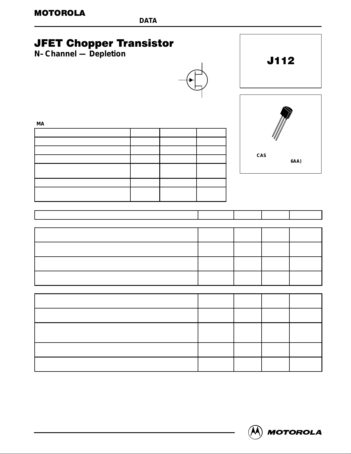
MOTOROLA J112RLRA, J112RL1, J112 Datasheet

SEMICONDUCTOR TECHNICAL DATA
N–Channel — Depletion
GATE
MAXIMUM RATINGS
Rating Symbol Value Unit
Drain–Gate Voltage V
Gate–Source Voltage V
Gate Current I
Total Device Dissipation @ TA = 25°C
Derate above 25°C
Lead Temperature T
Operating and Storage Junction
T emperature Range
P
TJ, T
DG
GS
G
D
L
stg
–65 to +150 °C
1 DRAIN
3
2 SOURCE
–35 Vdc
–35 Vdc
50 mAdc
350
2.8
300 °C
mW
mW/°C
Order this document
1
2
3
CASE 29–04, STYLE 5
TO–92 (TO–226AA)
by J112/D
ELECTRICAL CHARACTERISTICS (T
Characteristic
OFF CHARACTERISTICS
Gate–Source Breakdown Voltage
(IG = –1.0 µAdc)
Gate Reverse Current
(VGS = –15 Vdc)
Gate Source Cutoff Voltage
(VDS = 5.0 Vdc, ID = 1.0 µAdc)
Drain–Cutoff Current
(VDS = 5.0 Vdc, VGS = –10 Vdc)
ON CHARACTERISTICS
Zero–Gate–Voltage Drain Current
(VDS = 15 Vdc)
Static Drain–Source On Resistance
(VDS = 0.1 Vdc)
Drain Gate and Source Gate On–Capacitance
(VDS = VGS = 0, f = 1.0 MHz)
Drain Gate Off–Capacitance
(VGS = –10 Vdc, f = 1.0 MHz)
Source Gate Off–Capacitance
(VGS = –10 Vdc, f = 1.0 MHz)
1. Pulse Width = 300 µs, Duty Cycle = 3.0%.
(1)
= 25°C unless otherwise noted)
A
Symbol Min Max Unit
V
(BR)GSS
I
GSS
V
GS(off)
I
D(off)
I
DSS
r
DS(on)
C
dg(on)
+
C
sg(on)
C
dg(off)
C
sg(off)
35 — Vdc
— –1.0 nAdc
–1.0 –5.0 Vdc
— 1.0 nAdc
5.0 — mAdc
— 50 Ω
— 28 pF
— 5.0 pF
— 5.0 pF
(Replaces J111/D)
Motorola Small–Signal Transistors, FETs and Diodes Device Data
Motorola, Inc. 1997
1

J112
TYPICAL SWITCHING CHARACTERISTICS
1000
500
200
100
RK = RD′
TJ = 25°C
V
GS(off)
= 7.0 V
50
20
10
, TURN–ON DELAY TIME (ns)
5.0
d(on)
t
RK = 0
2.0
1.0
0.5 0.7 1.0 2.0 3.0 5.0 7.0 10 20 30 50
ID, DRAIN CURRENT (mA)
Figure 1. T urn–On Delay Time
1000
500
200
100
50
RK = RD′
20
10
, TURN–OFF DELAY TIME (ns)
5.0
d(off)
t
2.0
1.0
0.5 0.7 1.0 2.0 3.0 5.0 7.0 10 20 30 50
RK = 0
ID, DRAIN CURRENT (mA)
V
GS(off)
TJ = 25°C
= 7.0 V
1000
500
200
RK = RD′
V
GS(off)
TJ = 25°C
= 7.0 V
100
50
20
, RISE TIME (ns)
r
10
5.0
RK = 0
2.0
1.0
0.5 0.7 1.0 2.0 3.0 5.0 7.0 10 20 30 50
ID, DRAIN CURRENT (mA)
Figure 2. Rise Time
1000
500
V
= 7.0 V
200
RK = RD′
100
50
20
, FALL TIME (ns) t
f
10
t
RK = 0
5.0
2.0
1.0
0.5 0.7 1.0 2.0 3.0 5.0 7.0 10 20 30 50
ID, DRAIN CURRENT (mA)
GS(off)
TJ = 25°C
Figure 3. Turn–Off Delay Time
R
GEN
50
Ω
V
GEN
INPUT PULSE
t
r
t
PULSE WIDTH
DUTY CYCLE
f
INPUT
≤
0.25 ns
≤
0.5 ns
= 2.0
≤
2.0%
SET V
R
K
50
Ω
RGG
µ
s
DS(off)
&
R
Ȁ+
D
R
R
= 10 V
GG
V
GG
K
RD(RT)
R
D
Figure 5. Switching Time Test Circuit
Figure 4. Fall Time
NOTE 1
The switching characteristics shown above were measured using a
+V
DD
R
D
R
T
OUTPUT
50
Ω
50)
)
RT)
50
test circuit similar to Figure 5. At the beginning of the switching
interval, the gate voltage is at Gate Supply Voltage (–VGG). The
Drain–Source Voltage (VDS) is slightly lower than Drain Supply
Voltage (VDD) due to the voltage divider. Thus Reverse Transfer
Capacitance (C
VGG + VDS.
) or Gate–Drain Capacitance (Cgd) is charged to
rss
During the turn–on interval, Gate–Source Capacitance (Cgs)
discharges through the series combination of R
must discharge to V
parallel combination of effective load impedance (R′D) an d
through RG and RK in series with the
DS(on)
and RK. C
Gen
gd
Drain–Source Resistance (rds). During the turn–off, this charge flow
is reversed.
Predicting turn–on time is somewhat difficult as the channel
resistance rds is a function of the gate–source voltage. While C
discharges, VGS approaches zero and rds decreases. Since C
discharges through rds, turn–on time is non–linear. During turn–off,
gs
gd
the situation is reversed with rds increasing as Cgd charges.
The above switching curves show two impedance conditions;
1) RK is equal to RD, which simulates the switching behavior of
cascaded stages where the driving source impedance is normally
the load impedance of the previous stage, and 2) RK = 0 (low
impedance) the driving source impedance is that of the generator.
2
Motorola Small–Signal Transistors, FETs and Diodes Device Data
 Loading...