


Advance Information
DSP56366/D
Rev. 1.6, 01/2004
24-Bit Audio Digital
Signal Processor
Freescale Semiconductor, Inc.
Topic Page
Overview ............................ .........i
Signal/Connection
Descriptions ....................... 1-1
nc...
Specifications .......................... 2-1
I
Packaging .................... ...........3-1
Design Considerations ...........4-1
Ordering Information ...............5-1
Power Consumption
Benchmark ....................... A-1
IBIS Model .............................B-1
cale Semiconductor,
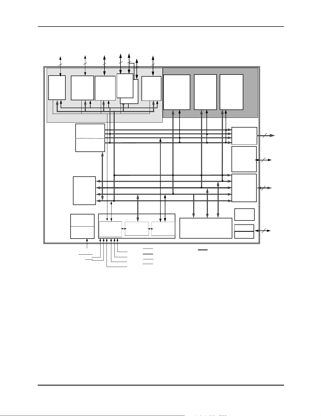
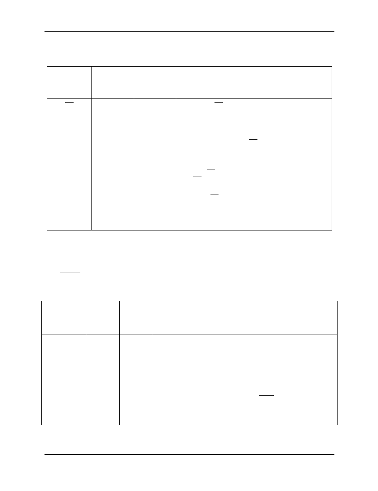
Overview
The DSP56366 supports digital audio applications requiring sound field processing,
acoustic equalization, and other digital audio algorithms. The DSP56366 uses the
high performance, single-clock-per-cycle DSP56300 core family of programmable
CMOS digital signal processors (DSPs) combined with the audio signal processing
capability of the Motorola Symphony™ DSP family, as shown in Figure 1. This
design provides a two-fold performance increase over Motorola’s popular
Symphony family of DSPs while retaining code compatibility. Significant
architectural enhancements include a barrel shifter, 24-bit addressing, instruction
cache, and direct memory access (DMA). The DSP56366 offers 120 million
instructions per second (MIPS) using an internal 120 MHz clock at 3.3 V.
Data Sheet Conventions
This data sheet uses the following conventions:
OVERBAR
“asserted” Means that a high true (active high) signal is high or that a low
“deasserted” Means that a high true (active high) signal is low or that a low
Used to indicate a signal that is active when pulled low (For
example, the RESET
true (active low) signal is low
true (active low) signal is high
pin is active when low.)
Frees
This document contains information on a new product. Specifications and information herein are subject to change without notice.
IMOTOROLA DSP56366 Advance Information i
Examples: Signal/
Symbol
PIN
PIN False Deasserted VIH / V
PIN True Asserted VIH / V
PIN False Deasserted VIL / V
Note: *Values for VIL, VOL, VIH, and VOH are defined by individual product
specifications.
Logic State Signal State Voltage*
True Asserted VIL / V
OL
OH
OH
OL
For More Information On This Product,
Go to: www.freescale.com
Freescale Semiconductor, Inc.
Overview
Features
4
1
TRIPLE
TIMER
nc...
I
CLOCK
cale Semiconductor,
2
DAX
(SPDIF
Tx.)
ADDRESS
GENERATI
SIX
CHANNEL
INTER
NAL
PLL
EXTAL
RESET
PINIT/NMI
16
HOST
INTER
PROGR
AM
8
ESAI
INTER-
FACE
ESAI_1
PERIPHERAL
EXPANSION AREA
PIO_EB
24-BIT
DSP563
PROGR
AM
MODA/IRQA
MODB/IRQB
MODC/IRQC
MODD/IRQD
6
SHI
INTER
5
PROGRA
M RAM
/INSTR.
CACHE
3K x 24
PROGR
AM
MEMORY EXPANSION AREA
X
MEMOR
Y
RAM
13K X
PM_EB
YAB
XAB
PAB
DAB
DDB
YDB
XDB
PDB
GDB
DATA ALU
24X24+56->56-BIT
Figure 1 DSP56366 Block Diagram
Y
MEMOR
Y
RAM
7K X 24
XM_EB
24 BITS BUS
YM_EB
EXTERNAL
ADDRESS
BUS
SWITCH
DRAM &
SRAM
BUS
EXTERN
AL
DATA
POWE
JTAG
OnCE
18
ADDRESS
10
CONTROL
24
DATA
4
Frees
1 Features
1.1 DSP56300 Modular Chassis
• 120 Million Instructions Per Second (MIPS) with an 120 MHz clock at 3.3V.
• Object Code Compatible with the 56K core.
• Data ALU with a 24 x 24 bit multiplier-accumulator and a 56-bit barrel shifter. 16-bit arithmetic
support.
• Program Control with position independent code support and instruction cache support.
• Six-channel DMA controller.
ii DSP56366 Advance Information MOTOROLA
For More Information On This Product,
Go to: www.freescale.com

Freescale Semiconductor, Inc.
• PLL based clocking with a wide range of frequency multiplications (1 to 4096), predivider factors (1
to 16) and power saving clock divider (2
• Internal address tracing support and OnCE for Hardware/Software debugging.
• JTAG port.
• Very low-power CMOS design, fully static design with operating frequencies down to DC.
• STOP and WAIT low-power standby modes.
i
: i=0 to 7). Reduces clock noise.
Overview
Features
1.2 On-chip Memory Configuration
• 7Kx24 Bit Y-Data RAM and 8Kx24 Bit Y-Data ROM.
• 13Kx24 Bit X-Data RAM and 32Kx24 Bit X-Data ROM.
• 40Kx24 Bit Program ROM.
• 3Kx24 Bit Program RAM and 192x24 Bit Bootstrap ROM. 1K of Program RAM may be used as
nc...
I
Instruction Cache or for Program ROM patching.
• 2Kx24 Bit from Y Data RAM and 5Kx24 Bit from X Data RAM can be switched to Program RAM
resulting in up to 10Kx24 Bit of Program RAM.
cale Semiconductor,
Frees
1.3 Off-chip Memory Expansion
• External Memory Expansion Port.
• Off-chip expansion up to two 16M x 24-bit word of Data memory.
• Off-chip expansion up to 16M x 24-bit word of Program memory.
• Simultaneous glueless interface to SRAM and DRAM.
1.4 Peripheral Modules
• Serial Audio Interface (ESAI): up to 4 receivers and up to 6 transmitters, master or slave. I2S, Sony,
AC97, network and other programmable protocols.
• Serial Audio Interface I(ESAI_1): up to 4 receivers and up to 6 transmitters, master or slave. I
Sony, AC97, network and other programmable protocols
The ESAI_1 shares four of the data pins with ESAI, and ESAI_1 does NOT support HCKR and
HCKT (high frequency clocks)
• Serial Host Interface (SHI): SPI and I
support for 8, 16 and 24-bit words.
• Byte-wide parallel Host Interface (HDI08) with DMA support.
• Triple Timer module (TEC).
• Digital Audio Transmitter (DAX): 1 serial transmitter capable of supporting the SPDIF, IEC958,
CP-340 and AES/EBU digital audio formats.
• Pins of unused peripherals (except SHI) may be programmed as GPIO lines.
2
C protocols, multi master capability, 10-word receive FIFO,
2
S,
1.5 Packaging
• 144-pin plastic LQFP package.
MOTOROLA DSP56366 Advance Information iii
For More Information On This Product,
Go to: www.freescale.com
Overview
Documentation
Freescale Semiconductor, Inc.
2 Documentation
Table 1 lists the documents that provide a complete description of the DSP56366 and are required to
design properly with the part. Documentation is available from a local Motorola distributor, a Motorola
semiconductor sales office, a Motorola Literature Distribution Center, or through the Motorola DSP home
page on the Internet (the source for the latest information).
Table 1 DSP56366 Documentation
Document Name Description Order Number
DSP56300 Family Manual Detailed description of the 56000-family
architecture and the 24-bit core processor
and instruction set
DSP56366 User’s Manual Detailed description of memory, peripher-
nc...
I
DSP56366 Technical Data Sheet Electrical and timing specifications; pin
DSP56366 Product Brief Brief description of the chip DSP56366P/D
als, and interfaces
and package descriptions
cale Semiconductor,
DSP56300FM/AD
DSP56366UM/D
DSP56366/D
Frees
iv DSP56366 Advance Information MOTOROLA
For More Information On This Product,
Go to: www.freescale.com

Freescale Semiconductor, Inc.
SECTION 1
SIGNAL/CONNECTION DESCRIPTIONS
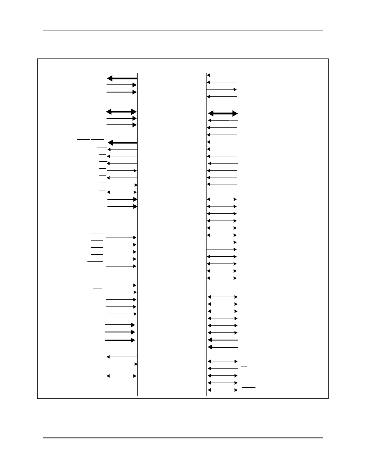
1.1 SIGNAL GROUPI NG S
The input and output signals of the DSP56366 are organized into functional groups, which are listed in
Table 1-1 and illustrated in Figure 1-1.
The DSP56366 is operated from a 3.3 V supply; however, some of the inputs can tolerate 5 V. A special
notice for this feature is added to the signal descriptions of those inputs.
Table 1-1 DSP56366 Functional Signal Groupings
nc...
I
cale Semiconductor,
Frees
Functional Group
Power (VCC)
Ground (GND)
Clock and PLL
Address bus
1
Data bus 24 Figure 1-6
Bus control 10 Figure 1-7
Interrupt and mode control 5 Figure 1-8
HDI08
SHI 5 Figure 1-10
ESAI
ESAI_1
Digital audio transmitter (DAX)
Port A
Port B
Port C
Port E
Port D
2
3
5
4
Number of
Signals
20
18
3
18 Figure 1-5
16 Table 1-9
12 Table 1-11
6 Table 1-12
2 Table 1-13
Detailed
Description
Figure 1-2
Figure 1-3
Figure 1-4
Timer 1 Table 1-14
JTAG/OnCE Port 4 Figure 1-15
Notes: 1. Port A is the external memory interface po rt, inc luding the ex ternal addres s bus, d ata bu s, a nd co ntrol
signals.
2. Port B signals are the GPIO port signals which are multiplexed with the HDI08 signals.
3. Port C signals are the GPIO port signals which are multiplexed with the ESAI signals.
4. Port D signals are the GPIO port signals which are multiplexed with the DAX signals.
5. Port E signals are the GPIO port signals which are multiplexed with the ESAI_1 signals.
MOTOROLA DSP56366 Advance Information 1-1
For More Information On This Product,
Go to: www.freescale.com
Freescale Semiconductor, Inc.
Signal/Connection Descriptions
Signal Groupings
nc...
I
cale Semiconductor,
Frees
PORT A ADDRESS BUS
A0-A17
VCCA (3)
GNDA (4)
PORT A DATA BUS
D0-D23
VCCD (4)
GNDD (4)
PORT A BUS CONTROL
AA0-AA2/RAS0-RAS2
CAS
RD
WR
TA
BR
BG
BB
VCCC (2)
GNDC (2)
INTERRUPT AND
MODE CONTROL
MODA/IRQA
MODB/IRQB
MODC/IRQC
MODD/IRQD
RESET
PLL AND CLOCK
EXTAL
PINIT/NMI
PCAP
VCCP
GNDP
QUIET POWER
VCCQH (3)
VCCQL (4)
GNDQ (4)
SPDIF TRANSMITTER (DAX)
ADO [PD1]
ACI [PD0]
TIMER 0
TIO0 [TIO0]
DSP56366
Port D
Port B
Port C
Port E
OnCE ON-CHIP EMULATION/
TDI
TCK
TDO
TMS
JTAG PORT
PARALLEL HOST PORT (HDI08)
HAD(7:0) [PB0-PB7]
HAS/HA0 [PB8]
HA8/HA1 [PB9]
HA9/HA2 [PB10]
HRW/HRD [PB11]
HDS/HWR [PB12]
HCS/HA10 [PB13]
HOREQ/HTRQ [PB14]
HACK/HRRQ [PB15]
VCCH
GNDH
SERIAL AUDIO INTERFACE (ESAI)
SCKT[PC3]
FST [PC4]
HCKT [PC5]
SCKR [PC0]
FSR [PC1]
HCKR [PC2]
SDO0[PC11] / SDO0_1[PE11]
SDO1[PC10] / SDO1_1[PE10]
SDO2/SDI3[PC9] / SDO2_1/SDI3_1[PE9]
SDO3/SDI2[PC8] / SDO3_1/SDI2_1[PE8]
SDO4/SD I1 [PC7]
SDO5/SD I0 [PC6]
SERIAL AUDIO INTERFACE(ESAI_1)
SCKT_1[PE3]
T_1[PE4]
FS
SCKR_1[PE0]
FSR_1[PE1]
SDO4_1/SDI1_1[PE7]
SDO5_1/SDI0_1[PE6]
VCCS (2)
GNDS (2)
SERIAL HOST INTERFACE (SHI)
MOSI/HA0
/HA2
SS
MISO/SDA
SCK/SCL
HREQ
Figure 1-1 Signals Identified by Functional Group
1-2 DSP56366 Advance Information MOTOROLA
For More Information On This Product,
Go to: www.freescale.com

1.2 POWER
Freescale Semiconductor, Inc.
Signal/Connection Descriptions
Table 1-2 Power Inputs
Power
nc...
I
cale Semiconductor,
Frees
Power
Name
V
CCP
V
V
(4) Quiet Core (Low) Power—V
CCQL
(3) Quiet External (High) Power—V
CCQH
V
(3) Address Bus Power—V
CCA
(4) Data Bus Power—V
V
CCD
V
(2) Bus Control Power—V
CCC
V
CCH
(2) SHI, ESAI, ESAI_1, DAX and Timer Power —V
V
CCS
PLL Power—V
and the input should be provided with an extremely low impedance path to the V
power rail. There is one V
This input must be tied externally to all other chip power inputs. The user must provide
adequate external decoupling capacitors. There are four V
must be tied externally to all other chip power inputs. The user must provide adequate
decoupling capacitors. There are three V
drivers. This input must be tied externally to all other chip power inputs. The user must
provide adequate external decoupling capacitors. There are three V
This input must be tied externally to all other chip power inputs. The user must provide
adequate external decoupling capacitors. There are four V
input must be tied externally to all other chip power inputs. The user must provide adequate external decoupling capacitors. There are two V
Host Power—V
tied externally to all other chip power inputs. The user must provide adequate external
decoupling capacitors. There is one V
ESAI, ESAI_1, DAX and Timer. This input must be tied externally to all other chip
power inputs. The user must provide adequate external decoupling capacitors. There
are two V
CCS
is VCC dedicated for PLL use. The voltage should be well-regulated
CCP
input.
CCP
CCQL
is an isolated power for sections of the address bus I/O
CCA
is an isolated power for sections of the data bus I/O drivers.
CCD
is an isolated power for the bus control I/O drivers. This
CCC
is an isolated power for the HDI08 I/O drivers. This input must be
CCH
inputs.
Description
CC
is an isolated power for the internal processing logic.
inputs.
CCQL
is a quiet power source for I/O lines. This input
CCQH
inputs.
CCQH
inputs.
CCA
inputs.
CCD
inputs.
CCC
input.
CCH
is an isolated power for the SHI,
CCS
MOTOROLA DSP56366 Advance Information 1-3
For More Information On This Product,
Go to: www.freescale.com

Freescale Semiconductor, Inc.
Signal/Connection Descriptions
Ground
1.3 GROUND
Table 1-3 Grounds
nc...
I
cale Semiconductor,
Frees
Ground
Name
GND
P
(4) Quiet Ground—GNDQ is an isolated ground for the internal processing logic. This con-
GND
Q
GND
(4) Addr ess Bus Ground—GNDA is an isolated ground for sections of the address bus
A
GND
(4) Data Bus Ground—GNDD is an isolated ground for sections of the data bus I/O driv-
D
(2) Bus Control Ground—GNDC is an isolated ground for the bus control I/O drivers. This
GND
C
GND
H
GND
(2) SHI, ESAI, ESAI_1, DAX and Timer Ground—GNDS is an isolated ground for the SHI,
S
PLL Ground—GNDP is a ground dedicated for PLL use. The connection should be
provided with an extremely low-impedance path to ground. V
to GND
There is one GND
nection must be tied externally to all other chip ground connections. The user must provide adequate external decoupling capacitors. There are four GND
I/O drivers. This connection must be tied externally to all other chip ground connections. The user must provide adequate external decoupling capacitors. There are four
GND
ers. This connection must be tied externally to all other chip ground connections. The
user must provide adequate external decoupling capacitors. There are four GND
nections.
connection must be tied externally to all other chip ground connections. The user must
provide adequate external decoupling capacitors. There are two GND
Host Ground—GNDh is an isolated ground for the HD08 I/O drivers. This connection
must be tied externally to all other chip ground connections. The user must provide
adequate external decoupling capacitors. There is one GND
ESAI, ESAI_1, DAX and Timer. This connection must be tied externally to all other chip
ground connections. The user must provide adequate external decoupling capacitors.
There are two GND
by a 0.47 µF capacitor located as close as possible to the chip package.
P
connections.
A
connection.
P
connections.
S
Description
should be bypassed
CCP
connections.
Q
connections.
C
connection.
H
con-
D
1-4 DSP56366 Advance Information MOTOROLA
For More Information On This Product,
Go to: www.freescale.com

Freescale Semiconductor, Inc.
1.4 CLOCK AND PLL
Table 1-4 Clock and PLL Signals
Signal/Connection Descriptions
Clock and PLL
Signal
Name
EXTAL Input Input External Clock Input—An external clock source must be connected
PCAP Input Input PLL Capacitor—PCAP is an input connecting an off-chip capacitor
nc...
I
PINIT/N
MI
Type
Input Input PLL Initial/Nonmaskable Interrupt—During assertion of RESET,
cale Semiconductor,
State
during
Reset
Signal Description
to EXTAL in order to supply the clock to the internal clock generator
and PLL.
This input cannot tolerate 5 V.
to the PLL filter. Connect one capacitor terminal to PCAP and the
other terminal to V
If the PLL is not used, PCAP may be tied to V
ing.
the value of PINIT/NMI
PLL control register, determining whether the PLL is enabled or disabled. After RESET
cessing, the PINIT/NMI
negative-edge-trigge red nonma sk ab le int erru pt (NM I) reque st inte r nally synchronized to internal system clock.
This input cannot tolerate 5 V.
.
CCP
, GND, or left float-
CC
is written into the PLL Enable (PEN) bit of the
de assertion and during normal instruction pro-
Schmitt-trigger input is a
Frees
MOTOROLA DSP56366 Advance Information 1-5
For More Information On This Product,
Go to: www.freescale.com

Freescale Semiconductor, Inc.
Signal/Connection Descriptions
External Memory Expansion Port (Port A)
1.5 EXTERNAL MEMORY EXPANSION PORT (PORT A)
When the DSP56366 enters a low-power standby mode (stop or wait), it releases bus mastership and
tri-states the relevant port A signals: A0–A17, D0–D23, AA0/RAS0
1.5.1 External Add ress Bu s
Table 1-5 External Address Bus Signals
–AA2/RAS2, RD, WR, BB, CAS.
Signal
Name
nc...
I
A0–A17 Output Tri-stated Address Bus—When the DSP is the bus master, A0–A17 are
Type
State
during
Reset
Signal Description
active-high outputs that specify the address for external program
and data memory accesses. Otherwise, the signals are tri-stated.
To minimize power dissipation, A0–A17 do not change state when
external memory spaces are not being accessed.
1.5.2 External Dat a Bus
Table 1-6 External Data Bus Signals
Signal
Name
D0–D23 Input/Output Tri-stated Data Bus—When the DSP is the bus master, D0–D23 are
Type
cale Semiconductor,
State
during
Reset
Signal Description
active-high, bidirectional input/outputs that provide the bidirectional data bus for external program and data memory
accesses. Otherwise, D0–D23 are tri-stated.
Frees
1-6 DSP56366 Advance Information MOTOROLA
For More Information On This Product,
Go to: www.freescale.com
Freescale Semiconductor, Inc.
1.5.3 External Bus C ontrol
Table 1-7 External Bus Control Signals
Signal/Connection Descriptions
External Memory Expansion Port (Port A)
Signal
Name
AA0–AA2/
RAS0
–RAS2
nc...
I
CAS
RD
WR
Type
Output Tri-stated Address Attribute or Row Address Strobe—When
Output Tri-stated Column Address Strobe— When the DSP is the bus
Output Tri-stated Read Enable—When the DSP is the bus master, RD
Output Tri-stated Write Enable—When the DSP is the bus master, WR
cale Semiconductor,
State
during
Reset
Signal Description
defined as AA, these signals can be used as chip
selects or additional address lines. When defined as
RAS
, these signals can be used as RAS for DRAM
interface. These signals are tri-statable outputs with
programmable polarity.
master, CAS
strobe the column address. Otherwise, if the bus mastership enable (BME) bit in the DRAM control register
is cleared, the signal is tri-stated.
is an active-low output that is asserted to read external
memory on the data bus (D0-D23). Otherwise, RD
tri-stated.
is an active-low output that is asserted to write external memory on the data bus (D0-D23). Otherwise, WR
is tri-stated.
is an active-l ow ou tp ut us ed by DRAM t o
is
Frees
MOTOROLA DSP56366 Advance Information 1-7
For More Information On This Product,
Go to: www.freescale.com

Freescale Semiconductor, Inc.
Signal/Connection Descriptions
External Memory Expansion Port (Port A)
Table 1-7 External Bus Control Signals (continued)
Signal
Name
TA Input Ignored
nc...
I
Type
cale Semiconductor,
State
during
Reset
Input
Signal Description
Transfer Acknowledge—If the DSP is the bus master
and there is no external bus activity, or the DSP is not
the bus master, the TA
is a data transfer acknowledge (DTACK) function that
can extend an external bus cycle indefinitely. Any
number of wait states (1, 2. . .infinity) may be added to
the wait states inserted by the BCR by keeping TA
deasserted. In typical operation, TA
the start of a bus cycle, is asserted to enable completion of the bus cycle, and is deasserted before the next
bus cycle. The current bus cycle completes one clock
period after TA
system clock. The number of wait states is determined
by the TA
whichever is longer. The BCR can be used to set the
minimum number of wait states in external bus cycles.
In order to use the TA
programmed to at least one wait state. A zero wait
state access cannot be extended by TA
otherwise improper operation may result. TA
ate synchronously or asynchronously, depending on
the setting of the TAS bit in the operating mode register (OMR).
TA
functionality may not be used while performing
DRAM type accesses, otherwise improper operation
may result.
is asserted synchronous to the internal
input or by the bus control register (BCR),
input is ignored. The TA input
is deasserted at
functionality, the BCR must be
deassertion,
can oper-
Frees
1-8 DSP56366 Advance Information MOTOROLA
For More Information On This Product,
Go to: www.freescale.com

Freescale Semiconductor, Inc.
Table 1-7 External Bus Control Signals (continued)
Signal/Connection Descriptions
External Memory Expansion Port (Port A)
Signal
Name
BR Output Output
nc...
I
BG
Type
Input Ignored
cale Semiconductor,
State
during
Reset
(deasserted)
Input
Signal Description
Bus Request—BR is an active-low output, never
tri-stated. BR
mastership. BR
needs the bus. BR
independent of whether the DSP56366 is a bus master or a bus sl av e. B us “p ar ki ng ” al l ow s BR
serted even though the DSP56366 is the bus master.
(See the description of bus “parking” in the BB
description.) The bus request hol d (BR H) bit in the
BCR allows BR
even though the DSP does not need the bus. BR
typically sent to an external bus arbitrator that controls
the priority, parking, and tenure of each master on the
same external bus. BR
requests for the external bus, never for the internal
bus. During hardware reset, BR
arbitration is reset to the bus slave state.
Bus Grant—BG is an active-low inpu t. BG is as serte d
by an external bus arbitration circuit when the
DSP56366 becomes the next bus master. When BG
asserted, the DSP56366 must wait until BB
serted before taking bus mastership. When BG
deasserted, bus mastership is typically given up at the
end of the current bus cycle. This may occur in the
middle of an instruction that requires more than one
external bus cycle for execution.
For proper BG
tration enable bit (ABE) in the OMR register must be
set.
is asserted when the DSP requests bus
is deasserted when the DSP no longer
may be asserted or deasserted
to be deas-
signal
to be asserted under software control
is
is only affected by DSP
is deasserted and the
is
is deas-
is
operation, the asynchronous bus arbi-
Frees
MOTOROLA DSP56366 Advance Information 1-9
For More Information On This Product,
Go to: www.freescale.com
Freescale Semiconductor, Inc.
Signal/Connection Descriptions
Interrupt and Mode Control
Table 1-7 External Bus Control Signals (continued)
Signal
Name
BB
nc...
I
Type
Input/Output Input Bus Busy—BB is a bidirectional active-low input/out-
1.6 INTERRUPT AND MODE CONTROL
The interrupt and mode control signals select the chip’s operating mode as it comes out of hardware reset.
After RESET
cale Semiconductor,
Signal
Name
is deasserted, these inputs are hardware interrupt request lines.
State
Type
during
Reset
State
during
Reset
put. BB
is deasserted can the pending bus master become the
bus master (and then assert the signal again). The bus
master may keep BB
ity regardless of whether BR
serted. This is called “bus parking” and allows the
current bus master to reuse the bus without rearbitration until another device requires the bus. The deassertion of BB
(i.e., BB
by an external pull-up resistor).
For proper BB
tration enable bit (ABE) in the OMR register must be
set.
BB
Table 1-8 Interrupt and Mode Control
indicates that the bus is active. Only after BB
is driven high and then released and held high
requires an external pull-up resistor.
Signal Description
asserted after ceasing bus activ-
is done by an “active pull-up” method
operation, the asynchronous bus arbi-
Signal Description
is asserted or deas-
Frees
MODA/IRQA Input Input Mode Select A/External Interrupt Request A—MODA/IRQA is
an active-low Schmitt-trigger input, internally synchronized to the
DSP clock. MODA/IRQA
during hardware reset and becomes a level-sensitive or negative-edge-triggered, maskable interrupt request input during normal instruction processing. MODA, MODB, MODC, and MODD
select one of 16 initial chip operating modes, latched into the
OMR when the RESET
the stop standby state and the MODA/IRQA
the processor will exit the stop state.
This input is 5 V tolerant.
1-10 DSP56366 Advance Information MOTOROLA
selects the initial chip operating mode
signal is deasserted. If the processor is in
pin is pulled to GND,
For More Information On This Product,
Go to: www.freescale.com
Freescale Semiconductor, Inc.
Table 1-8 Interrupt and Mode Control (continued)
Signal/Connection Descriptions
Interrupt and Mode Control
nc...
I
cale Semiconductor,
Frees
Signal
Name
MODB/IRQB Input Input Mode Select B/External Interrupt Request B—MODB/IRQB is
MODC/IRQC
MODD/IRQD
RESET
Type
Input Input Mode Select C/External Interrupt Request C—MODC/IRQC is
Input Input Mode Select D/External Interrupt Request D—MODD/IRQD is
Input Input Reset—RESET is an active-low, Schmitt-trigger input. When
State
during
Reset
Signal Description
an active-low Schmitt-trigger input, internally synchronized to the
DSP clock. MODB/IRQB
during hardware reset and becomes a level-sensitive or negative-edge-triggered, maskable interrupt request input during normal instruction processing. MODA, MODB, MODC, and MODD
select one of 16 initial chip operating modes, latched into OMR
when the RESET
This input is 5 V tolerant.
an active-low Schmitt-trigger input, internally synchronized to the
DSP clock. MODC/IRQC
during hardware reset and becomes a level-sensitive or negative-edge-triggered, maskable interrupt request input during normal instruction processing. MODA, MODB, MODC, and MODD
select one of 16 initial chip operating modes, latched into OMR
when the RESET
This input is 5 V tolerant.
an active-low Schmitt-trigger input, internally synchronized to the
DSP clock. MODD/IRQD
during hardware reset and becomes a level-sensitive or negative-edge-triggered, maskable interrupt request input during normal instruction processing. MODA, MODB, MODC, and MODD
select one of 16 initial chip operating modes, latched into OMR
when the RESET
This input is 5 V tolerant.
asserted, the chip is placed in the Reset state and the internal
phase generator is reset. The Schmitt-trigger input allows a slowly
rising input (such as a capacitor charging) to reset the chip reliably. When the RESET
ating mode is latched from the MODA, MODB, MODC, and
MODD inputs. The RESET
up. A stable EXTAL signal must be supplied while RESET
asserted.
signal is deasserted.
signal is deasserted.
signal is deasserted.
selects the initial chip operating mode
selects the initial chip operating mode
selects the initial chip operating mode
signal is deasserted, the initial chip oper-
signal must be asserted during power
is being
This input is 5 V tolerant.
MOTOROLA DSP56366 Advance Information 1-11
For More Information On This Product,
Go to: www.freescale.com

Freescale Semiconductor, Inc.
Signal/Connection Descriptions
PARALLEL HOST INTERFACE (HDI08)
1.7 PARALLEL HOST INTERFACE (HDI08)
The HDI08 provides a fast, 8-bit, parallel data port that may be connected directly to the host bus. The
HDI08 supports a variety of standard buses and can be directly connected to a number of industry
standard microcomputers, microprocessors, DSPs, and DMA hardware.
Table 1-9 Host Interface
nc...
I
cale Semiconductor,
Frees
Signal Name Type
H0–H7 Input/
output
HAD0–HAD7 Input/
output
PB0–PB7 Input, outp ut,
or
disconnected
HA0 Input GPIO
HAS/
HAS Input GPIO
State during
Reset
GPIO
disconnected
GPIO
disconnected
GPIO
disconnected
disconnected
disconnected
Signal Description
Host Data—When HDI08 is programmed t o interface a
nonmultiplexed host bus and the HI funct ion is sel ected,
these signals are lines 0–7 of the bidirectional, tri-state
data bus.
Host Address/Data—When HDI08 is programmed to
interface a multiplexed host bus and the HI function is
selected, these signals are lines 0–7 of the address/data
bidirectional, multiplexed, tri-state bus.
Port B 0–7—When the HDI08 is configured as GPIO,
these signals are individually programmable as input, output, or internally disconnected.
The default state after reset for these signals is GPIO disconnected.
These inputs are 5 V tolerant.
Host Address Input 0—When the HDI08 is programmed
to interface a nonmultiplexed host bus and the HI function
is selected, this signal is line 0 of the host addres s inp ut
bus.
Host Address Strobe—When HDI08 is programmed to
interface a multiplexed host bus and the HI function is
selected, this signal is the host address strobe (HAS)
Schmitt-trigger input. The polarity of the address strobe is
programmable, but is configured active-low (HAS
ing reset.
) follow-
PB8 Input, output,
or
disconnected
1-12 DSP56366 Advance Information MOTOROLA
GPIO
disconnected
Port B 8—When the HDI08 is configured as GPIO, this
signal is individually programmed as input, output, or
internally disconnected.
The default state after reset for this signal is GPIO disconnected.
This input is 5 V tolerant.
For More Information On This Product,
Go to: www.freescale.com

Freescale Semiconductor, Inc.
Table 1-9 Host Interface (continued)
Signal/Connection Descriptions
PARALLEL HOST INTERFACE (HDI08)
nc...
I
cale Semiconductor,
Frees
Signal Name Type
HA1 Input GPIO
HA8 Input GPIO
PB9 Input, output,
or
disconnected
HA2 Input GPIO
HA9 Input GPIO
PB10 Input, Output,
or
Disconnected
State during
Reset
disconnected
disconnected
GPIO
disconnected
disconnected
disconnected
GPIO
disconnected
Signal Description
Host Address Input 1—When the HDI08 is programmed
to interface a nonmultiplexed host bus and the HI function
is selected, this signal is line 1 of the host address (HA1)
input bus.
Host Address 8—When HDI08 is programmed to interface a multiplexed host bus and the HI function is
selected, this signal is line 8 of the host address (HA8)
input bus.
Port B 9—When the HDI08 is configured as GPIO, this
signal is individually programmed as input, output, or
internally disconnected.
The default state after reset for this signal is GPIO disconnected.
This input is 5 V tolerant.
Host Address Input 2—When the HDI08 is programmed
to interface a non-multiplexed host bus and the HI function is selected, this signal is line 2 of the host address
(HA2) input bus.
Host Address 9—When HDI08 is programmed to interface a multiplexed host bus and the HI function is
selected, this signal is line 9 of the host address (HA9)
input bus.
Port B 10—When the HDI08 is configured as GPIO, this
signal is individually programmed as input, output, or
internally disconnected.
The default state after reset for this signal is GPIO disconnected.
This input is 5 V tolerant.
MOTOROLA DSP56366 Advance Information 1-13
For More Information On This Product,
Go to: www.freescale.com
Freescale Semiconductor, Inc.
Signal/Connection Descriptions
PARALLEL HOST INTERFACE (HDI08)
Table 1-9 Host Interface (continued)
nc...
I
cale Semiconductor,
Frees
Signal Name Type
HRW Input GPIO
HRD
/
HRD
PB11 Input, Output,
HDS
/
HDS
HWR
/
HWR
PB12 In put, outp ut,
Input GPIO
or
Disconnected
Input GPIO
Input GPIO
or
disconnected
State during
Reset
disconnected
disconnected
GPIO
disconnected
disconnected
disconnected
GPIO
disconnected
Signal Description
Host Read/Write—When HDI08 is programmed to inter-
face a single-data-strobe host bus and the HI function is
selected, this signal is the Host Read/Write
Host Read Data—When HDI08 is programmed to interface a double-data-strobe host bus and the HI function is
selected, this signal is the host read data strobe (HRD)
Schmitt-trigger input. The polarity of the data strobe is
programmable, but is configured as active-low (HRD
after reset.
Port B 11—When the HDI08 is configured as GPIO, this
signal is individually programmed as input, output, or
internally disconnected.
The default state after reset for this signal is GPIO disconnected.
This input is 5 V tolerant.
Host Data Strobe—When HDI08 is programmed to inter-
face a single-data-strobe host bus and the HI function is
selected, this signal is the host data strobe (HDS)
Schmitt-trigger input. The polarity of the data strobe is
programmable, but is configured as active-low (HDS
lowing reset.
Host Write Data—When HDI08 is programmed to interface a double-data-strobe host bus and the HI function is
selected, this signal is the host write data strobe (HWR)
Schmitt-trigger input. The polarity of the data strobe is
programmable, but is configured as active-low (HWR
lowing reset.
Port B 12—When the HDI08 is configured as GPIO, this
signal is individually programmed as input, output, or
internally disconnected.
(HRW) input.
)
) fol-
) fol-
The default state after reset for this signal is GPIO disconnected.
This input is 5 V tolerant.
1-14 DSP56366 Advance Information MOTOROLA
For More Information On This Product,
Go to: www.freescale.com

Freescale Semiconductor, Inc.
Table 1-9 Host Interface (continued)
Signal/Connection Descriptions
PARALLEL HOST INTERFACE (HDI08)
nc...
I
cale Semiconductor,
Frees
Signal Name Type
HCS Input GPIO
HA10 Input GPIO
PB13 Input, output,
or
disconnected
HOREQ
HOREQ
HTRQ
HTRQ
/
/
PB14 Input, output,
Output GPIO
Output GPIO
or
disconnected
State during
Reset
disconnected
disconnected
GPIO
disconnected
disconnected
disconnected
GPIO
disconnected
Signal Description
Host Chip Select—When HDI08 is programmed to inter-
face a nonmultiplexed host bus and the HI function is
selected, this signal is the host chip select (HCS) input.
The polarity of the chip select is programmable, but is
configured active-low (HCS
Host Address 10—When HDI08 is programmed to interface a multiplexed host bus and the HI function is
selected, this signal is line 10 of the host address (HA10)
input bus.
Port B 13—When the HDI08 is configured as GPIO, this
signal is individually programmed as input, output, or
internally disconnected.
The default state after reset for this signal is GPIO disconnected.
This input is 5 V tolerant.
Host Request—When HDI08 is programmed to interface
a single host request host bus and the HI function is
selected, this signal is the host request (HOREQ) output.
The polarity of the host request is programmable, but is
configured as active-low (HOREQ
host request may be programmed as a driven or
open-drain output.
Transmit Host Request—When HDI08 is programmed
to interface a double host request host bus and the HI
function is selected, this signal is the transmit host
request (HTRQ) output. The polarity of the host request is
programmable, but is configured as active-low (HTRQ
following reset. The host request may be programmed as
a driven or open-drain output.
Port B 14—When the HDI08 is configured as GPIO, this
signal is individually programmed as input, output, or
internally disconnected.
) after reset.
) following reset. The
)
The default state after reset for this signal is GPIO disconnected.
This input is 5 V tolerant.
MOTOROLA DSP56366 Advance Information 1-15
For More Information On This Product,
Go to: www.freescale.com

Freescale Semiconductor, Inc.
Signal/Connection Descriptions
PARALLEL HOST INTERFACE (HDI08)
Table 1-9 Host Interface (continued)
Signal Name Type
HACK/
HACK
/
HRRQ
HRRQ
nc...
I
PB15 In put, outp ut,
Input GPIO
Output GPIO
or
disconnected
cale Semiconductor,
State during
Reset
disconnected
disconnected
GPIO
disconnected
Signal Description
Host Acknowledge—When HDI08 is programmed to
interface a single host request host bus and the HI function is selected, this signal is the host acknowledge
(HACK) Schmitt-trigger input. The polarity of the host
acknowledge is programmable, but is configured as
active-low (HACK
Receive Host Request—When HDI08 is programmed to
interface a double host request host bus and the HI function is selected, this signal is the receive host request
(HRRQ) output. The polarity of the host request is programmable, but is configured as active-low (HRRQ
reset. The host request may be programmed as a driven
or open-drain output.
Port B 15—When the HDI08 is configured as GPIO, this
signal is individually programmed as input, output, or
internally disconnected.
The default state after reset for this signal is GPIO disconnected.
This input is 5 V tolerant.
) after reset .
) after
Frees
1-16 DSP56366 Advance Information MOTOROLA
For More Information On This Product,
Go to: www.freescale.com

Freescale Semiconductor, Inc.
Signal/Connection Descriptions
Serial Host Interface
1.8 SERIAL HOST INTERFACE
The SHI has five I/O signals that can be configured to allow the SHI to operate in either SPI or I2C mode.
Table 1-10 Serial Host Interface Signals
nc...
I
cale Semiconductor,
Frees
Signal
Name
SCK Input or
SCL Input or
MISO Input or
SDA Input or
Signal
Type
output
output
output
open-drain
output
State during
Reset
Tri-stated SPI Serial Clock—The SCK signal is an output when the SPI is config-
ured as a master and a Schmitt-trigger input when the SPI is configured
as a slave. When the SPI is configured as a master, the SCK signal is
derived from the internal SHI clock generator. When the SPI is configured as a slave, the SCK signal is an input, and the clock signal from
the external master synchronizes the data transfer. The SCK signal is
ignored by the SPI if it is defined as a slave and the slave select (SS
signal is not asserted. In both the master and slave SPI devices, data is
shifted on one edge of the SCK signal and is sampled on the opposite
edge where data is stable. Edge polarity is determined by the SPI
transfer protocol.
Tri-stated I
Tri-stated
Tri-stated I2C Data and Acknowledge—In I2C mode, SDA is a Schmitt-trigger
2
C Serial Clock—SCL carries the clock for I2C bus transactions in the
2
I
C mode. SCL is a Schmitt-trigger input when configured as a slave
and an open-drain output when configured as a master. SCL should be
connected to V
This signal is tri-stated during hardware, software, and individual reset.
Thus, there is no need for an external pull-up in this state.
This input is 5 V tolerant.
SPI Master-In-Slave-Out
MISO is the master data input line. The MISO signal is used in conjunction with the MOS I sign a l for tran sm itt ing an d rec eivin g serial da ta. T h is
signal is a Schmitt-trig ger inp u t whe n co nf igure d fo r the SP I M a ste r
mode, an output when configured for the SPI Slave mode, and tri-stated
if configured for the SPI Slave mode when SS
pull-up resistor is not required for SPI operation.
input when receiving and an open-drain output when transmitting. SDA
should be connected to V
data for I
high period of SCL. The data in SDA is only allowed to change when
SCL is low. When the bus is free, SDA is high. The SDA line is only
allowed to change during the time SCL is high in the case of start and
stop events. A high-to-low transition of the SDA line while SCL is high is
a unique situation, and is defined as the start event. A low-to-high transition of SDA while SCL is high is a unique situation defined as the stop
event.
This signal is tri-stated during hardware, software, and individual reset.
Thus, there is no need for an external pull-up in this state.
2
C transactions. The data in SDA must be stable during the
through a pull-up resistor.
CC
Signal Description
—When the SPI is configured as a master,
is deasserted. An external
through a pull-up resistor. SDA carries the
CC
)
This input is 5 V tolerant.
MOTOROLA DSP56366 Advance Information 1-17
For More Information On This Product,
Go to: www.freescale.com

Freescale Semiconductor, Inc.
Signal/Connection Descriptions
Serial Host Interface
Table 1-10 Serial Host Interface Signals (continued)
nc...
I
cale Semiconductor,
Frees
Signal
Name
MOSI Input or
HA0 Input I2C Slave Address 0—This signal uses a Schmitt-trigger input when
SS
HA2 Input I
HREQ
Signal
Type
output
Input Tri-stated SPI Slave Select—This signal is an active low Schmitt-trigger input
Input or
Output
State during
Reset
Tri-stated
Tri-stated Host Request—This signal is an active low Schmitt-trigger input when
SPI Master-Out-Slave-In
MOSI is the m a ster d a ta o utpu t line . The MOSI signal is u se d in co nju n ction with the MISO signal for transmitting and receiving serial data. MOSI
is the slave d ata input line when the SPI is configure d as a slave . This
signal is a Schmitt-trigger input when configured for the SPI Slave mode.
configured for the I
HA0 signal is used to form the slave device address. HA0 is ignored
when configured for the I
This signal is tri-stated during hardware, software, and individual reset.
Thus, there is no need for an external pull-up in this state.
This input is 5 V tolerant.
when configured for the SPI mode. When configured for the SPI Slave
mode, this signal is used to enable the SPI slave for transfer. When
configured for the SPI master mode, this signal should be kept deasserted (pulled high). If it is asserted while configured as SPI master, a
bus error condition is flagged. If SS
clocks and keeps the MISO output signal in the high-impedance state.
2
C Slave Address 2—This signal uses a Schmitt-trigger input when
configured for the I
the HA2 signal is used to form the slave device address. HA2 is ignored
in the I
This signal is tri-stated during hardware, software, and individual reset.
Thus, there is no need for an external pull-up in this state.
This input is 5 V tolerant.
configured for the master mode but an active low output when configured for the slave mode.
When configured for the slave mode, HREQ
the SHI is ready for the next data word transfer and deasserted at the
first clock pulse of the new data word transfer. When configured for the
master mode, HREQ
device, it will trigger the start of the data word transfer by the master.
After finishing the data word transfer, the master will await the next
assertion of HREQ
This signal is tri-stated during hardware, software, personal reset, or
when the HREQ1–HREQ0 bits in the HCSR are cleared. There is no
need for external pull-up in this state.
This input is 5 V tolerant.
2
C master mode.
Signal Description
—When the SPI is configured as a master,
2
C mode. When configured for I2C slave mode, the
2
C master mode.
is deasserted, the SHI ignores SCK
2
C mode. When configured for the I2C Slave mode,
is asserted to indicate that
is an input. When asserted by the external slave
to proceed to the next transfer.
1-18 DSP56366 Advance Information MOTOROLA
For More Information On This Product,
Go to: www.freescale.com

Freescale Semiconductor, Inc.
Signal/Connection Descriptions
Enhanced Serial Audio Interface
1.9 ENHANCED SERIAL AUDIO INTERFACE
Table 1-11 Enhanced Serial Audio Interface Signals
Signal
Name
HCKR Input or output GPIO
nc...
I
PC2 Input, output,
HCKT Input or output GPIO
PC5 Input, output,
Signal Type
or
disconnected
or
disconnected
cale Semiconductor,
State during
Reset
disconnected
GPIO
disconnected
disconnected
GPIO
disconnected
Signal Description
High Frequency Clock for Receiver
input, this signal provides a high frequency clock source for the
ESAI receiver as an alternate to the DSP core clock. When programmed as an output, this signal can serve as a high-frequency
sample clock (e.g., for external digital to analog converters
[DACs]) or as an additional system clock.
Port C 2
individually programmable as input, output, or internally disconnected.
The default state after reset is GPIO disconnected.
This input is 5 V tolerant.
High Frequency Clock for Transmitter—When programmed as an input, this signal provides a high frequency
clock source for the ESAI transmitter as an alternate to the
DSP core clock. When programmed as an output, this signal
can serve as a high frequency sample clock (e.g., for external
DACs) or as an additional system clock.
Port C 5—When the ESAI is configured as GPIO, this signal
is individually programmable as input, output, or internally disconnected.
The default state after reset is GPIO disconnected.
This input is 5 V tolerant.
—When the E S AI is co n figure d as G P IO , this sign al is
—When programmed as an
Frees
MOTOROLA DSP56366 Advance Information 1-19
For More Information On This Product,
Go to: www.freescale.com

Freescale Semiconductor, Inc.
Signal/Connection Descriptions
Enhanced Serial Audio Interface
Table 1-11 Enhanced Serial Audio Interface Signals (continued)
nc...
I
cale Semiconductor,
Frees
Signal
Name
FSR Input or output GPIO
PC1 Input, output,
FST Input or output GPIO
PC4 Input, output,
Signal Type
or
disconnected
or
disconnected
State during
Reset
disconnected
GPIO
disconnected
disconnected
Signal Description
Frame Sync for Receiver—This is the receiver frame sync
input/output signal. In the asynchronous mode (SYN=0), the
FSR pin operates as the frame sync input or output used by
all the enabled receivers. In the synchronous mode (SYN=1),
it operates as either the serial flag 1 pin (TEBE=0), or as the
transmitter external buffer enable control (TEBE=1, RFSD=1).
When this pin is configured as serial flag pin, its direction is
determined by the RFSD bit in the RCCR register. When configured as the output flag OF1, this pin will reflect the value of
the OF1 bit in the SAICR register, and the data in the OF1 bit
will show up at the pin synchronized to the frame sync in normal mode or the slot in network mode. When configured as
the input flag IF1, the data value at the pin will be stored in the
IF1 bit in the SAISR register, synchronized by the frame sync
in normal mode or the slot in network mode.
Port C 1—When the ESAI is configured as GPIO, this signal
is individually programmable as input, output, or internally disconnected.
The default state after reset is GPIO disconnected.
This input is 5 V tolerant.
Frame Sync for Transmitter—This is the transmitter frame
sync input/output signal. For synchronous mode, this signal is
the frame sync for both transmitters and receivers. For asynchronous mode, FST is the frame sync for the transmitters
only. The direction is determined by the transmitter frame
sync direction (TFSD) bit in the ESAI transmit clock control
register (TCCR).
Port C 4—When the ESAI is configured as GPIO, this signal
is individually programmable as input, output, or internally disconnected.
The default state after reset is GPIO disconnected.
This input is 5 V tolerant.
1-20 DSP56366 Advance Information MOTOROLA
For More Information On This Product,
Go to: www.freescale.com

Freescale Semiconductor, Inc.
Table 1-11 Enhanced Serial Audio Interface Signals (continued)
Signal/Connection Descriptions
Enhanced Serial Audio Interface
Signal
Name
SCKR Input or output GPIO
nc...
I
PC0 Input, output,
SCKT Input or output GPIO
PC3 Input, output,
cale Semiconductor,
Signal Type
or
disconnected
or
disconnected
State during
Reset
disconnected
GPIO
disconnected
disconnected
GPIO
disconnected
Signal Description
Receiver Serial Clock—SCKR provides the receiver serial
bit clock for the ESAI. The SCKR operates as a clock input or
output used by all the enabled receivers in the asynchronous
mode (SYN=0), or as serial flag 0 pin in the synchronous
mode (SYN=1).
When this pin is configured as serial flag pin, its direction is
determined by the RCKD bit in the RCCR register. When configured as the output flag OF0, this pin will reflect the value of
the OF0 bit in the SAICR register, and the data in the OF0 bit
will show up at the pin synchronized to the frame sync in normal mode or the slot in network mode. When configured as
the input flag IF0, the data value at the pin will be stored in the
IF0 bit in the SAISR register, synchronized by the frame sync
in normal mode or the slot in network mode.
Port C 0—When the ESAI is configured as GPIO, this signal
is individually programmable as input, output, or internally disconnected.
The default state after reset is GPIO disconnected.
This input is 5 V tolerant.
Transmitter Serial Clock—This signal provides the serial bit
rate clock for the ESAI. SCKT is a clock input or output used
by all enabled transmitters and receivers in synchronous
mode, or by all enabled transmitters in asynchronous mode.
Port C 3—When the ESAI is configured as GPIO, this signal
is individually programmable as input, output, or internally disconnected.
The default state after reset is GPIO disconnected.
This input is 5 V tolerant.
Frees
SDO5 Output GPIO
disconnected
SDI0 Input GPIO
disconnected
PC6 Input, output,
or
disconnected
MOTOROLA DSP56366 Advance Information 1-21
GPIO
disconnected
Serial Data Output 5—When programmed as a transmitter,
SDO5 is used to transmit data from the TX5 serial transmit
shift register.
Serial Data In put 0
used to receive serial data into the RX0 serial receive shift register.
Port C 6—When the ESAI is configured as GPIO, this signal
is individually programmable as input, output, or internally disconnected.
The default state after reset is GPIO disconnected.
This input is 5 V tolerant.
—When programmed as a receiver, SDI0 is
For More Information On This Product,
Go to: www.freescale.com

Freescale Semiconductor, Inc.
Signal/Connection Descriptions
Enhanced Serial Audio Interface
Table 1-11 Enhanced Serial Audio Interface Signals (continued)
nc...
I
cale Semiconductor,
Frees
Signal
Name
SDO4 Output GPIO
SDI1 Input GPIO
PC7 Input, output,
SDO3/S
DO3_1
SDI2/
SDI2_1
PC8/PE8 Input, output,
Signal Type
or
disconnected
Output GPIO
Input GPIO
or
disconnected
State during
Reset
disconnected
disconnected
GPIO
disconnected
disconnected
disconnected
GPIO
disconnected
Signal Description
Serial Data Output 4—When programmed as a transmitter,
SDO4 is used to transmit data from the TX4 serial transmit
shift register.
Serial Data Input 1—When programmed as a receiver, SDI1
is used to receive serial data into the RX1 serial receive shift
register.
Port C 7—When the ESAI is configured as GPIO, this signal
is individually programmable as input, output, or internally disconnected.
The default state after reset is GPIO disconnected.
This input is 5 V tolerant.
Serial Data Output 3—When programmed as a transmitter,
SDO3 is used to transmit data from the TX3 serial transmit
shift register.
When enabled for ESAI_1 operation, this is the ESAI_1 Serial
Data Output 3.
Serial Data Input 2—When programmed as a receiver, SDI2
is used to receive serial data into the RX2 serial receive shift
register.
When enabled for ESAI_1 operation, this is the ESAI_1 Serial
Data Input 2.
Port C 8—When the ESAI is configured as GPIO, this signal
is individually programmable as input, output, or internally disconnected.
When enabled for ESAI_1 GPIO, this is the Port E 8 signal.
The default state after reset is GPIO disconnected.
This input is 5 V tolerant.
1-22 DSP56366 Advance Information MOTOROLA
For More Information On This Product,
Go to: www.freescale.com

Freescale Semiconductor, Inc.
Table 1-11 Enhanced Serial Audio Interface Signals (continued)
Signal/Connection Descriptions
Enhanced Serial Audio Interface
Signal
Name
SDO2/
SDO2_1
SDI3/SDI
3_1
nc...
I
PC9/PE9 Input, output,
SDO1/
SDO1_1
PC10/
PE10
Signal Type
Output GPIO
Input GPIO
or
disconnected
Output GPIO
Input, output,
or
disconnected
cale Semiconductor,
State during
Reset
disconnected
disconnected
GPIO
disconnected
disconnected
GPIO
disconnected
Signal Description
Serial Data Output 2—When programmed as a transmitter,
SDO2 is used to transmit data from the TX2 serial transmit
shift register.
When enabled for ESAI_1 operation, this is the ESAI_1 Serial
Data Output 2.
Serial Data Input 3—When programmed as a receiver, SDI3
is used to receive serial data into the RX3 serial receive shift
register.
When enabled for ESAI_1 operation, this is the ESAI_1 Serial
Data Input 3.
Port C 9—When the ESAI is configured as GPIO, this signal
is individually programmable as input, output, or internally disconnected.
When enabled for ESAI_1 GPIO, this is the Port E 9 signal.
The default state after reset is GPIO disconnected.
This input is 5 V tolerant.
Serial Data Output 1—SDO1 is used to transmit data from
the TX1 serial transmit shift register.
When enabled for ESAI_1 operation, this is the ESAI_1 Serial
Data Output 1.
Port C 10—When the ESAI is configured as GPIO, this signal
is individually programmable as input, output, or internally disconnected.
When enabled for ESAI_1 GPIO, this is the Port E 10 signal.
The default state after reset is GPIO disconnected.
This input is 5 V tolerant.
Frees
SDO0/S
DO0_1
PC11/
PE11
MOTOROLA DSP56366 Advance Information 1-23
Output GPIO
disconnected
Input, output,
or
disconnected
disconnected
GPIO
Serial Data Output 0—SDO0 is used to transmit data from
the TX0 serial transmit shift register.
When enabled for ESAI_1 operation, this is the ESAI_1 Serial
Data Output 0.
Port C 11—When the ESAI is configured as GPIO, this signal
is individually programmable as input, output, or internally disconnected.
When enabled for ESAI_1 GPIO, this is the Port E 11 signal.
The default state after reset is GPIO disconnected.
This input is 5 V tolerant.
For More Information On This Product,
Go to: www.freescale.com

Freescale Semiconductor, Inc.
Signal/Connection Descriptions
Enhanced Serial Audio Interface_1
ENHANCED SERIAL AUDIO INTERFACE_1
Table 1-12 Enhanced Serial Audio Interface_1 Signals
nc...
I
cale Semiconductor,
Frees
Signal
Name
FSR_1 Input or output GPIO
PE1 Input, output,
FST_1 Input or output GPIO
Signal Type
or
disconnected
State during
Reset
disconnected
GPIO
disconnected
disconnected
Signal Description
Frame Sync for Receiver_1—This is the receiver frame sync
input/output signal. In the asynchronous mode (SYN=0), the
FSR pin operates as the frame sync input or output used by all
the enabled receivers. In the synchronous mode (SYN=1), it
operates as either the serial flag 1 pin (TEBE=0), or as the
transmitter external buffer enable control (TEBE=1, RFSD=1).
When this pin is configured as serial flag pin, its direction is
determined by the RFSD bit in the RCCR register. When configured as the output flag OF1, this pin will reflect the value of
the OF1 bit in the SAICR register, and the data in the OF1 bit
will show up at the pin synchronized to the frame sync in normal mode or the slot in network mode. When configured as the
input flag IF1, the data value at the pin will be stored in the IF1
bit in the SAISR register, synchronized by the frame sync in
normal mode or the slot in network mode.
Port E 1—When the ESAI is configured as GPIO, this signal is
individually programmable as input, output, or internally disconnected.
The default state after reset is GPIO disconnected.
This input cannot tolerate 5 V.
Frame Sync for Transmitter_1—This is the transmitter frame
sync input/output signal. For synchronous mode, this signal is
the frame sync for both transmitters and receivers. For asynchronous mode, FST is the frame sync for the transmitters
only. The direction is determined by the transmitter frame sync
direction (TFSD) bit in the ESAI transmit clock control register
(TCCR).
PE4 Input, output,
or
disconnected
1-24 DSP56366 Advance Information MOTOROLA
GPIO
disconnected
Port E 4—When the ESAI is configured as GPIO, this signal is
individually programmable as input, output, or internally disconnected.
The default state after reset is GPIO disconnected.
This input cannot tolerate 5 V.
For More Information On This Product,
Go to: www.freescale.com

Freescale Semiconductor, Inc.
Table 1-12 Enhanced Serial Audio Interface_1 Signals
Signal/Connection Descriptions
Enhanced Serial Audio Interface_1
nc...
I
cale Semiconductor,
Frees
Signal
Name
SCKR_1 Input or output GPIO
PE0 Input, output,
SCKT_1 Input or output GPIO
PE3 Input, output,
SDO5_1 Output GPIO
Signal Type
or
disconnected
or
disconnected
State during
Reset
disconnected
GPIO
disconnected
disconnected
GPIO
disconnected
disconnected
Signal Description
Receiver Serial Clock_1—SCKR provides the receiver serial
bit clock for the ESAI. The SCKR operates as a clock input or
output used by all the enabled receivers in the asynchronous
mode (SYN=0), or as serial flag 0 pin in the synchronous mode
(SYN=1).
When this pin is configured as serial flag pin, its direction is
determined by the RCKD bit in the RCCR register. When configured as the output flag OF0, this pin will reflect the value of
the OF0 bit in the SAICR register, and the data in the OF0 bit
will show up at the pin synchronized to the frame sync in normal mode or the slot in network mode. When configured as the
input flag IF0, the data value at the pin will be stored in the IF0
bit in the SAISR register, synchronized by the frame sync in
normal mode or the slot in network mode.
Port E 0—When the ESAI is configured as GPIO, this signal is
individually programmable as input, output, or internally disconnected.
The default state after reset is GPIO disconnected.
This input cannot tolerate 5 V.
Transmitter Serial Clock_1—This signal provides the serial
bit rate clock for the ESAI. SCKT is a clock input or output used
by all enabled transmitters and receivers in synchronous mode,
or by all enabled transmitters in asynchronous mode.
Port E 3—When the ESAI is configured as GPIO, this signal is
individually programmable as input, output, or internally disconnected.
The default state after reset is GPIO disconnected.
This input cannot tolerate 5 V.
Serial Data Output 5_1
SDO5 is used to transmit data from the TX5 serial transmit shift register.
—When programmed as a transmitter,
SDI0_1 Input GPIO
disconnected
PE6 Input, output,
or
disconnected
MOTOROLA DSP56366 Advance Information 1-25
GPIO
disconnected
Serial Data Inpu t 0 _1
used to receive serial data into the RX0 serial receive shift register.
Port E 6
vidually programmable as input, output, or internally disconnected.
The default state after reset is GPIO disconnected.
This input cannot tolerate 5 V.
—When the ESAI is configured as GPIO, this signal is indi-
—When programmed as a receiver, SDI0 is
For More Information On This Product,
Go to: www.freescale.com

Freescale Semiconductor, Inc.
Signal/Connection Descriptions
spdif tRANSMITTER Digital Audio Interface
Table 1-12 Enhanced Serial Audio Interface_1 Signals
nc...
I
cale Semiconductor,
Frees
Signal
Name
SDO4_1 Output GPIO
SDI1_1 Input GPIO
PE7 Input, output,
Signal Type
or
disconnected
State during
Reset
disconnected
disconnected
GPIO
disconnected
Signal Description
Serial Data Output 4_1—When programmed as a transmitter,
SDO4 is used to transmit data from the TX4 serial transmit shift
register.
Serial Data Input 1_1—When programmed as a receiver,
SDI1 is used to receive serial data into the RX1 serial receive
shift register.
Port E 7—When the ESAI is configured as GPIO, this signal is
individually programmable as input, output, or internally disconnected.
The default state after reset is GPIO disconnected.
This input is 5 V tolerant.
1.10 SPDIF TRANSMITTER DIGITAL AUDIO INTERFACE
Table 1-13 Digital Audio Interface (DAX) Signals
Signal
Name
ACI Input GPIO
PD0 Input,
Type
output, or
disconnected
State During
Reset
Disconnected
GPIO
Disconnected
Signal Description
Audio Clock Input—This is the DAX clock input. When pro-
grammed to use an external clock, this input supplies the DAX
clock. The external clock frequency must be 256, 384, or 512
times the audio sampling frequency (256 × Fs, 384 × Fs or 512
× Fs, respectively).
Port D 0—When the DAX is configured as GPIO, this signal is
individually programmable as input, output, or internally disconnected.
The default state after reset is GPIO disconnected.
This input is 5 V tolerant.
ADO Output GPIO
Disconnected
PD1 Input,
output, or
disconnected
1-26 DSP56366 Advance Information MOTOROLA
GPIO
Disconnected
Digital Audio Data Output—This signal is an audio and
non-audio output in the form of AES/EBU, CP340 and IEC958
data in a biphase mark format.
Port D 1
vidually programmable as input, output, or internally disconnected.
The default state after reset is GPIO disconnected.
This input is 5 V tolerant.
—When the DAX is configured as GPIO, this signal is indi-
For More Information On This Product,
Go to: www.freescale.com

1.11 TIMER
Freescale Semiconductor, Inc.
Signal/Connection Descriptions
Table 1-14 Timer Signal
Timer
Signal
Name
TIO0 Input or
nc...
I
Type
Output
1.12 JTAG/OnCE INTERFACE
Signal
Name
cale Semiconductor,
TCK Input Input Test Clock—TCK is a test clock input signal used to synchronize the
Signal
Type
State
during
Reset
Input Timer 0 Schmitt-Trigger Input/Output—When timer 0 functions
as an external event counter or in measurement mode, TIO0 is
used as input. When timer 0 functions in watchdog, timer, or pulse
modulation mode, TIO0 is used as output.
The default mode after reset is GPIO input. This can be changed to
output or configured as a timer input/output through the timer 0
control/status register (TCSR0). If TIO0 is not being used, it is recommended to either define it as GPIO output immediately at the
beginning of operation or leave it defined as GPIO input but connected to Vcc through a pull-up resistor in order to ensure a stable
logic level at this input.
This input is 5 V tolerant.
Table 1-15 JTAG/OnCE Interface
State
during
Reset
JTAG test logic. It has an internal pull-up resistor.
This input is 5 V tolerant.
Signal Description
Signal Description
Frees
TDI Input Input Test Data Input—TDI is a test data serial input signal used for test
instructions and data. TDI is sampled on the rising edge of TCK and has
an internal pull-up resistor.
This input is 5 V tolerant.
TDO Output Tri-stated
TMS Input Input Test Mode Select—TMS is an input signal used to sequence the test con-
MOTOROLA DSP56366 Advance Information 1-27
Test Data Output
instructions and da ta. TD O is tri-stata ble and is actively drive n in the sh ift-IR
and shift-DR controller states. T DO changes on the falling edge of TCK.
troller’s state machine. TMS is sampled on the rising edge of TCK and has
an internal pull-up resistor.
This input is 5 V tolerant.
—TDO is a test data serial output signal used for test
For More Information On This Product,
Go to: www.freescale.com

Freescale Semiconductor, Inc.
nc...
I
cale Semiconductor,
Frees
THIS PAGE INTENTIONALLY LEFT BLANK
For More Information On This Product,
Go to: www.freescale.com

Freescale Semiconductor, Inc.
SECTION 2
SPECIFICATIONS
2.1 INTRODUCTION
The DSP56366 is a high density CMOS device with Transistor-Transistor Logic (TTL) compatible inputs
and outputs. The DSP56366 specifications are preliminary and are from design simulations, and may not
be fully tested or guaranteed. Finalized specifications will be published after full characterization and
device qualifications are complete.
2.2 MAXIMUM RATINGS
nc...
I
cale Semiconductor,
Frees
CAUTION
This device contains circuitry protecting
against damage due to high static voltage or
electrical fields. However, normal precautions
should be taken to avoid exceeding maximum
voltage ratings. Reliability of operation is
enhanced if unused inputs are pulled to an
appropriate logic voltage level (e.g., either
GND or V
pullup or pulldown resistor is 10 kΩ.
Note: In the calculation of timing requirements, adding a maximum value of one
specification to a minimum value of another specification does not yield a
reasonable sum. A maximum specification is calculated using a worst case
variation of process parameter values in one direction. The minimum
specification is calculated using the worst case for the same parameters in
the opposite direction. Therefore, a “maximum” value for a specification will
never occur in the same device that has a “minimum” value for another
specification; adding a maximum to a minimum represents a condition that
can never exist.
). The suggested value for a
CC
MOTOROLA DSP56366 Advance Information 2-1
For More Information On This Product,
Go to: www.freescale.com

Freescale Semiconductor, Inc.
Specifications
Thermal Characteristics
Table 2-1 Maximum Ratings
Rating
Supply Voltage V
All input voltages excluding “5 V tolerant” inputs
All “5 V tolerant” input voltages
Current drain per pin excluding V
Operating temperatur e range T
Storage temperature T
nc...
I
Notes: 1. GND = 0 V, VCC = 3.3 V ± 0.16 V, TJ = –40°C to +110°C, CL = 50 pF
2. Absolute maximum rati ngs are stres s ratings only, and functional operation at the maximum is not
guaranteed. Stress beyond the maximum rating may affect device reliability or cause permanent
damage to the device.
3. CAUTION: All “5 V Tolerant” input voltages must not be more than 3.95 V greater than the supply
voltage; this restriction applies to “power on”, as well as during normal operation. In any case, the
input voltages cannot be more than 5.75 V. “5 V Tolerant” inputs are inputs that tolerate 5 V.
1
3
and GND I 10 mA
CC
3
Symbol
CC
V
IN
V
IN5
J
STG
−0.3 to +4.0 V
GND -0.3 to VCC + 0.3 V
GND − 0.3 to VCC + 3.95 V
−40 to +110 °C
−55 to +125 °C
2.3 THERMAL CHARACTERISTICS
Table 2-2 Thermal Characteristics
Characteristic Symbol LQFP Value Unit
Junction-to-ambient thermal resistance
cale Semiconductor,
Junction-to-case thermal resistance
Thermal characterization parameter
1, 2
Natural Convection R
3
4
Natural Convection Ψ
R
θJA or θJA
θJC or θJC
JT
Value
1, 2
37 °C/W
7 °C/W
2.0 °C/W
Unit
Frees
Notes: 1. Junction temperature is a function of die size, on-chip power dissipation, package thermal resistance,
mounting site (board) temperature, ambient temperature, air flow, power dissipation of other
components on the board, and board thermal resistance.
2. Per SEMI G38-87 and JEDEC JESD51-2 with the single layer board horizontal.
3. Thermal resistance between the die and the case top surface as measured by the cold plate method
(MIL SPEC-883 Method 1012.1).
4. Thermal characterization parameter indi cating the tem peratu re di fferenc e betwee n pack age top and the
junction temperature per JEDEC JESD51-2. When Greek letters are not available, the thermal
characterization parameter is written as Psi-JT.
2-2 DSP56366 Advance Information MOTOROLA
For More Information On This Product,
Go to: www.freescale.com

Freescale Semiconductor, Inc.
2.4 DC ELECTRICAL CHARACTERISTICS
Table 2-3 DC Electrical Characteristics
Characteristics Symbol Min Typ Max Unit
Specifications
DC Electrical Characteristics
6
nc...
I
cale Semiconductor,
Frees
Supply voltage V
Input high voltage
• D(0:23), BG
•MOD
JTAG/ESAI/Timer/HDI08/DAX/ESAI_1
SDO4_1)
•SHI
(I2C mode)
•EXTAL
Input low voltage
• D(0:23), BG
•MOD
JTAG/ESAI/Timer/HDI08/DAX/ESAI_1
SDO4_1)
•SHI
(I2C mode)
•EXTAL
Input leakage current I
High impedance (off-state) input current
(@ 2.4 V / 0.4 V)
Output high voltage
• TTL (I
•CMOS (I
, BB, TA, ESAI_1
1
/IRQ1, RESET, PINIT/NMI and all
/SHI
(SPI mode)
V
8
, BB, TA, ESAI_1
1
/IRQ1, RESET, PINIT/NMI and all
/SHI
(SPI mode)
8
= –0.4 mA)
OH
= –10 µA)
OH
5,7
5
(except SDO4_1)
(except SDO4_1)
(only
(only
CC
V
IH
V
IHP
IHP
V
IHX
V
IL
V
ILP
V
ILP
V
ILX
IN
I
TSI
V
OH
3.14 3.3 3.46 V
2.0 — V
2.0 — V
1.5 — V
0.8 × V
VCC – 0.01 — — V
CC
–0.3 — 0.8
–0.3 — 0.8
–0.3 — 0.3 x V
–0.3 — 0.2 x V
–10 — 10 µA
–10 — 10 µA
2.4 — — V
—V
CC
CC
CC
+ 3.95
+ 3.95
CC
CC
CC
V
V
Output low voltage
• TTL (I
mA)
•CMOS (I
Internal supply curren t
120MHz
• In Normal mode
MOTOROLA DSP56366 Advance Information 2-3
= 3.0 mA, open-drain pins IOL = 6.7
OL
5,7
= 10 µA)
OL
5
2
at internal clock of
V
I
CCI
OL
V
——0.4
——0.01
— 116 200 mA
For More Information On This Product,
Go to: www.freescale.com

Freescale Semiconductor, Inc.
Specifications
AC Electrical Characteristics
Table 2-3 DC Electrical Characteristics6 (continued )
Characteristics Symbol Min Typ Max Unit
•In Wait mode I
• In Stop mode
PLL supply current — 1 2.5 mA
Input capacitance
Notes: 1. Refers to MODA/IRQA, MODB/IRQB, MODC/IRQC,and MODD/IRQD pins
2. Appendix A,
nc...
I
3. Deleted.
4. In order to obtain these results, all inputs, which are not disconnected at Stop mode, must be
5. Periodically sampled and not 100% tested
6. V
7. This characteristic does not apply to PCAP.
8. Driving EXTAL to the low V
4
5
Power Consumption Benchmark provides a formula to compute the es timated current
requirements in Normal mode. In order to obtain these results, all inputs must be terminated (i.e., not
allowed to float). Measurements are based on synthetic intensive DSP benchmarks. The power
consumption numbers in this specification are 90% of the measured results of this benchmark. This
reflects typical DSP applications. Typical internal supply current is measured with V
110°C. Maximum internal supply current is measured with V
terminated (i.e., not allowed to float).
= 3.3 V ± .16 V; TJ = – 40°C to +110°C, CL = 50 pF
CC
or the high V
current). To minimize power consumption, the minimum V
0.9 × V
and the maximum V
CC
IHX
should be no higher than 0.1 × VCC.
ILX
CCW
I
CCS
C
IN
value may cause additional power consumption (DC
ILX
2.5 AC ELECTRICAL CHARACTERISTICS
The timing waveforms shown in the AC electrical characteristics section are tested with a VIL maximum of
0.3 V and a V
cale Semiconductor,
in Note 8 of the previous table. AC timing specifications, which are referenced to a device input signal, are
measured in production with respect to the 50% point of the respective input signal’s transition. DSP56366
output levels are measured with the production test machine V
and 2.4 V, respectively.
minimum of 2.4 V for all pins except EXTAL, which is tested using the input levels shown
IH
—7.325mA
—110mA
——10pF
= 3.3 V at TJ =
= 3.46 V at TJ = 110°C.
CC
should be no lower than
IHX
and VOH reference levels set at 0.4 V
OL
CC
Frees
Note: Although the minimum value for the frequency of EXTAL is 0 MHz, the device
AC test conditions are 15 MHz and rated speed.
2-4 DSP56366 Advance Information MOTOROLA
For More Information On This Product,
Go to: www.freescale.com

Freescale Semiconductor, Inc.
2.6 INTERNAL CLOCKS
Table 2-4 Internal Clocks
Specifications
Internal Clocks
Expression
1, 2
Characteristics Symbol
Min Typ Max
Internal operation frequency with
PLL enabled
Internal operation frequency with
PLL disabled
nc...
I
cale Semiconductor,
Internal clock high period
• With PLL disabled — ET
• With PLL enabled and
MF ≤ 4
• With PLL enabled and
MF > 4
Internal clock low period
• With PLL disabled — ET
• With PLL enabled and
MF ≤ 4
• With PLL enabled and
MF > 4
Internal clock cycle time with PLL
enabled
f— (Ef × MF)/
(PDF × DF)
f — Ef/2 —
T
H
0.49 × ET
PDF × DF/MF
0.47 × ET
PDF × DF/MF
T
L
0.49 × ET
PDF × DF/MF
0.47 × ET
PDF × DF/MF
T
C
×
C
×
C
×
C
×
C
—ET
C
— 0.51 × ETC ×
PDF × DF/MF
— 0.53 × ETC ×
PDF × DF/MF
C
—0.51 × ETC ×
PDF × DF/MF
—0.53 × ETC ×
PDF × DF/MF
× PDF ×
C
DF/MF
—
—
—
—
Frees
Internal clock cycle time with PLL
disabled
Instruction cy cle t im e I
Notes: 1. DF = Division Factor
Ef = External frequency
= External clock cycle
ET
C
MF = Multiplication Factor
PDF = Predivision Factor
= internal clock cycle
T
C
2. See the PLL and Clock Generation section in the DSP56300 Family Manual for a detai led dis cussio n
of the PLL.
MOTOROLA DSP56366 Advance Information 2-5
T
CYC
C
—2 × ET
—TC—
C
—
For More Information On This Product,
Go to: www.freescale.com

Freescale Semiconductor, Inc.
Specifications
EXTERNAL CLOCK OPERATION
2.7 EXTERNAL CLOCK OPERATION
The DSP56366 system clock is an externally supplied square wave voltage source connected to EXTAL
(See Figure 2-1).
V
IHC
EXTAL
Midpoint
nc...
I
cale Semiconductor,
Frees
ETH
V
ILC
Note: The midpoint is 0.5 (V
2
4
IHC
ETL
+ V
3
ETC
ILC
).
Figure 2-1 External Clock Timing
Table 2-5 Clock Operation
No. Characteristics Symbol Min M ax
1 Frequency of EXTAL (EXTAL Pin Frequency)
The rise and fall time of this external clock should
be 3 ns maximum.
2 EXTAL input high
• With PLL disabled (46.7%–53.3% duty cycle4)
• With PLL enabled (42.5%–57.5% duty cycle
3 EXTAL input low
• With PLL disabled (46.7%–53.3% duty cycle4)
• With PLL enabled (42.5%–57.5% duty cycle
4 EXTAL cycle time
• With PLL disabled
1, 2
1, 2
2
4
) 3.54 ns 157.0 µs
4
) 3.54 ns 157.0 µs
Ef 0 120.0
ET
ET
ET
H
L
C
3.89 ns ∞
3.89 ns ∞
8.33 ns ∞
• With PLL enabled 8.33 ns 273.1 µs
32
7 Instruction cycle time = I
• With PLL disabled
• With PLL enabled 8.33 ns 8.53 µs
2-6 DSP56366 Advance Information MOTOROLA
CYC
= T
C
I
CYC
16.66 ns ∞
For More Information On This Product,
Go to: www.freescale.com

Freescale Semiconductor, Inc.
Table 2-5 Clock Operation (continued)
No. Characteristics Symbol Min Max
Notes: 1. Measured at 50% of the input transit ion
2. The maximum value for PLL enabled is given for minimum V
3. The maximum value for PLL enabled is given for minimum VCO and maximum DF.
4. The indicated duty cycle is for the specified maximum frequency for which a part is rated.
The minimum clock high or low time required for correct operation, however, remains the
same at lower operating frequencies; therefore, when a lower clock frequency is used, the
signal symmetry may vary from the specified duty cycle as long as the minimum high time
and low time requirements are met.
nc...
I
Specifications
EXTERNAL CLOCK OPERATION
and maximum MF.
CO
cale Semiconductor,
Frees
MOTOROLA DSP56366 Advance Information 2-7
For More Information On This Product,
Go to: www.freescale.com

Freescale Semiconductor, Inc.
Specifications
Phase Lock Loop (PLL) Characteristics
2.8 PHASE LOCK LOOP (PLL) CHARACTERISTICS
Table 2-6 PLL Characteristics
Characteristics Min Max Unit
nc...
I
cale Semiconductor,
Frees
VCO frequency when PLL enabled
(MF × E
PLL external capacitor (PCAP pin to V
•@ MF ≤ 4(MF × 580) − 100 (MF × 780) − 140
•@ MF > 4 MF × 830 MF × 1470
Notes: 1. C
× 2/PDF)
f
is the value of the PLL capacitor (connected between the PCAP pin and V
PCAP
recommended value in pF for C
(MF x 680)-120, for MF ≤ 4, or
MF x 1100, for MF > 4.
CCP
) (C
PCAP
1)
PCAP
can be computed from one of the following equations:
30 240 MHz
pF
). The
CCP
2.9 RESET, STOP, MODE SELECT, AND INTERRUPT TIMING
Table 2-7 Reset, Stop, Mode Select, and Interrupt Timing
No. Characteristics Expression Min Max Unit
8 Delay from RESET assertion to all pins at reset
9 Required RESET
3
value
duration
• Power on, external clock generato r, PLL
disabled
• Power on, external clock generato r, PLL
enabled
• During normal operation 2.5 × T
4
——26.0ns
50 × ET
1000 × ET
C
C
C
6
416.7 — ns
8.3 — µs
20.8 — ns
10 Delay from asynchronous RESET
to first external address output (internal reset
deassertion)
• Minimum
• Maximum 20.25 T
13 Mode select setup time 30.0 — ns
2-8 DSP56366 Advance Information MOTOROLA
5
deassertion
3.25 × TC + 2.0
+ 7.50 — 176.2 ns
C
29.1 — ns
For More Information On This Product,
Go to: www.freescale.com

Freescale Semiconductor, Inc.
Table 2-7 Reset, Stop, Mode Select, and Interrupt Timing6 (continued)
No. Characteristics Expression Min Max Unit
14 Mode select hold time 0.0 — ns
Specifications
Reset, Stop, Mode Select, and Interrupt Timing
nc...
I
cale Semiconductor,
Frees
15 Minimum edge-triggered interrupt request
assertion width
16 Minimum edge-triggered interrupt request deas-
sertion width
17 Delay from IRQA
assertion to external memory access address
out valid
• Caused by first interrupt instruction fetch
• Caused by first interrupt instruction execution 7.25 × T
18
Delay from
assertion to gen eral-purpose t ransfer ou tput valid
caused by first interrupt instruc tion execution
19 Delay from address output valid caused by first
interrupt instruction execute to interrupt request
deassertion for level sensitive fast interrupts
20 Delay from RD
deassertion for level sensitive fast interrupts
21 Delay from WR
deassertion for level sensitive fast interrupts
• DRAM for all WS (WS + 3.5) × T
• SRAM WS = 1 (WS + 3.5) × T
•SRAM WS = 2, 3 (WS + 3) × T
•SRAM WS ≥ 4 (WS + 2.5) × T
, IRQB, IRQC, IRQD, NMI
IRQA, IRQB, IRQC, IRQD, NMI
assertion to interrupt request
assertion to interrupt request
3.75 × T
1
3.25 × TC + WS × TC – 10.94 — Note 7 ns
1
1
5.5 — ns
5.5 — ns
4.25 × T
10 × TC + 5.0 88.3 — ns
+ WS × TC – 10.94 — Note 7 ns
C
+ 2.0 37.4 — ns
C
+ 2.0 62.4 — ns
C
– 10.94 — Note 7
C
– 10.94 — Note 7
C
– 10.94 — Note 7
C
– 10.94 — Note 7
C
ns
24 Duration for IRQA
Stop state
MOTOROLA DSP56366 Advance Information 2-9
assertion to recover from
4.9 —
For More Information On This Product,
Go to: www.freescale.com

Freescale Semiconductor, Inc.
Specifications
Reset, Stop, Mode Select, and Interrupt Timing
Table 2-7 Reset, Stop, Mode Select, and Interrupt Timing6 (continued )
No. Characteristics Expression Min Max Unit
25 Delay from IRQA assertion to fetch of first
instruction (when exiting Stop)
• PLL is not active during Stop (PCTL Bit 17 =
0) and Stop delay is enabled
(OMR Bit 6 = 0)
• PLL is not active during Stop (PCTL Bit 17 =
0) and Stop delay is not enabled (OMR Bit 6 =
1)
• PLL is active during Stop (PCTL Bit 17 = 1)
nc...
I
cale Semiconductor,
(Implies No Stop Delay)
26 Duration of level sensitive IRQA
ensure interrupt service (when exiting Stop)
• PLL is not active during Stop (PCTL Bit 17 =
0) and Stop delay is enabled
(OMR Bit 6 = 0)
• PLL is not active during Stop (PCTL Bit 17 =
0) and Stop delay is not enabled
(OMR Bit 6 = 1)
• PLL is active during Stop (PCTL Bit 17 = 1)
(implies no Stop delay)
27 Interrupt Requests Rate
• HDI08, ESAI, ESAI_1, SHI, DAX, Timer
•DMA 8T
•IRQ
, NMI (edge trigger) 8T
2, 3
assertion to
PLC × ET
PLC/2) × T
PLC × ET
0.5) × T
(8.25 ± 0.5) × T
2, 3
PLC × ET
PLC × ET
× PDF + (128 K −
C
C
× PDF + (23.75 ±
C
C
C
× PDF + (128K −
C
PLC/2) × T
× PDF + (20.5 ±
C
0.5) × T
5.5 × T
12T
C
C
C
C
C
C
——ms
——ms
64.6 72.9 ns
——ms
——ms
45.8 — ns
— 100.0 ns
—66.7ns
—66.7ns
Frees
•IRQ
(level trigger) 12T
28 DMA Requests Rate
• Data read from HDI08, ESAI, ESAI_1, SHI,
DAX
• Data write to HDI08, ESAI, ESAI_1, SHI, DAX 7T
• Timer 2T
•IRQ
, NMI (edge trigger) 3T
2-10 DSP56366 Advance Information MOTOROLA
6T
C
C
C
C
C
— 100.0 ns
—50.0ns
—58.0ns
16.7
—25.0ns
For More Information On This Product,
Go to: www.freescale.com

Freescale Semiconductor, Inc.
Specifications
Reset, Stop, Mode Select, and Interrupt Timing
Table 2-7 Reset, Stop, Mode Select, and Interrupt Timing6 (continued)
No. Characteristics Expression Min Max Unit
nc...
I
cale Semiconductor,
Frees
29 Delay from IRQA, IRQB, IRQC, IRQD, NMI
assertion to external memory (DMA source)
access address out valid
Notes: 1. When using fast interrupts and IRQA, IRQB, IRQC, an d I RQD are defined as level-sensitive, timings 19
through 21 apply to prevent multiple interrupt service. To avoid these timing restrictions, the deasserted
Edge-triggered mode is recommended when using fast interrupts. Long interrupts are recommended
when using Level-sensitive mode.
2. This timing depends on several settings:
For PLL disable, using external clock (PCTL Bit 16 = 1), no stabilization delay is required and recovery
time will be defined by the PCTL Bit 17 and OMR Bit 6 settings.
For PLL enable, if PCTL Bit 17 is 0, the PLL is shutd own during Stop. Recov ering from Stop requires the
PLL to get locked. The PLL lock procedure duration, PLL Lock Cycle s (PLC), may be in the range of 0 to
1000 cycles. This procedure occurs in parallel with the stop delay counter, and stop recovery will end
when the last of these two events o ccurs : th e s top delay counter co mp letes count or PLL loc k proc ed ure
completion.
PLC value for PLL disable is 0.
The maximum value for ET
120 MHz it is 4096/120 MHz = 34.1 µs). During the stabilization period, T
constant, and their width may vary, so timing may vary as well.
3. Periodically sampled and not 100% tested
4. RESET
5. If PLL does not lose lock
6. V
7. WS = number of wait states (measured in clock cycles, number of T
duration is measured during the time in which RESET is asserted, VCC is valid, and the EXTAL
input is active and valid. When the V
specified above) have not been yet met, the devi ce circuitry will be in an uninitial ized state that can result
in significant power consumption and heat-up. Designs should minimize this state to the shortest
possible duration.
= 3.3 V ± 0.16 V; TJ = –40°C to + 110°C, CL = 50 pF
CC
maximum value.
is 4096 (maximum MF) divided by the desired internal frequency (i.e., for
C
is valid, but the other “required RESET duration” conditions (as
CC
4.25 × TC + 2.0 37.4 — ns
, TH, and TL will not be
C
). Use expression to compute
C
MOTOROLA DSP56366 Advance Information 2-11
For More Information On This Product,
Go to: www.freescale.com

Freescale Semiconductor, Inc.
Specifications
Reset, Stop, Mode Select, and Interrupt Timing
RESET
9 10
8
V
IH
nc...
I
cale Semiconductor,
Frees
All Pins
A0–A17
A0–A17
RD
WR
IRQA, IRQB,
IRQC
, IRQD,
NMI
Reset Value
Figure 2-2 Reset Timing
First Interrupt Instruction
Execution/Fetch
20
21
1917
a) First Interrupt Instruction Execution
First Fetch
AA0460
General
Purpose
I/O
18
, IRQB,
IRQA
IRQC
, IRQD,
NMI
Figure 2-3 External Fast Interrupt Timing
2-12 DSP56366 Advance Information MOTOROLA
b) General Purpose I/O
For More Information On This Product,
Go to: www.freescale.com

Freescale Semiconductor, Inc.
IRQA, IRQB,
IRQC,
IRQD,
NMI
IRQA, IRQB,
IRQC,
IRQD,
NMI
Figure 2-4 External Interrupt Timing (Negative Edge-Triggered)
Reset, Stop, Mode Select, and Interrupt Timing
15
16
Specifications
AA0463
nc...
I
cale Semiconductor,
Frees
RESET
MODA, MODB,
MODC, MODD,
PINIT
IRQA
A0–A17
13
14
V
IH
V
IL
Figure 2-5 Operating Mode Select Timing
24
25
First Instruction Fetch
Figure 2-6 Recovery from Stop State Using IRQA
V
IH
V
IL
V
IH
IRQA, IRQB,
IRQD
, NMI
AA0465
AA0466
MOTOROLA DSP56366 Advance Information 2-13
For More Information On This Product,
Go to: www.freescale.com

Freescale Semiconductor, Inc.
Specifications
Reset, Stop, Mode Select, and Interrupt Timing
IRQA
26
25
A0–A17
Figure 2-7 Recovery from Stop State Using IRQA Interrupt Service
nc...
I
A0–A17
WR
IRQA, IRQB,
IRQC,
IRQD,
NMI
RD
29
First Interrupt Instruction Execution
Figure 2-8 External Memory Access (DMA Source) Timing
DMA Source Address
cale Semiconductor,
First IRQA Interrupt
Instruction Fetch
AA0467
AA1104
Frees
2-14 DSP56366 Advance Information MOTOROLA
For More Information On This Product,
Go to: www.freescale.com

Freescale Semiconductor, Inc.
External Memory Expansion Port (Port A)
2.10 EXTERNAL MEMORY EXPANSION PORT (PORT A)
2.10.1 SRAM Timing
Table 2-8 SRAM Read and Write Accesses3
Specifications
nc...
I
cale Semiconductor,
Frees
No. Characteristics Symbol
100 Address valid and AA assertion pulse width tRC, t
101 Address and AA valid to WR
102 WR
103 WR
assertion pulse width t
deassertion to address not valid t
assertion t
WC
AS
WP
WR
C
− 4.0
C
C
C
− 4.0
C
− 4.0
C
− 2.0
− 4.0
C
− 2.0
− 2.0
1
Expression
(WS + 1) × TC − 4.0
[1 ≤ WS ≤ 3]
(WS + 2) × T
[4 ≤ WS ≤ 7]
(WS + 3) × T
[WS ≥ 8]
0.25 × TC − 2.0
[WS = 1]
1.25 × T
[WS ≥ 4]
1.5 × TC − 4.0 [WS = 1] 8.5 — ns
All frequencies:
WS × T
[2 ≤ WS ≤ 3]
(WS − 0.5) × T
[WS ≥ 4]
0.25 × TC − 2.0
[1 ≤ WS ≤ 3]
1.25 × T
[4 ≤ WS ≤ 7]
2.25 × T
[WS ≥ 8]
Min Max Unit
12.0 — ns
46.0 — ns
87.0 — ns
0.1 — ns
8.4 — ns
12.7 — ns
25.2 — ns
0.1 — ns
8.4 — ns
16.7 — ns
All frequencies:
1.25 × T
[4 ≤ WS ≤ 7]
2.25 × T
[WS ≥ 8]
104 Address and AA valid to input data valid t
MOTOROLA DSP56366 Advance Information 2-15
AA
, t
(WS + 0.75) × TC − 7.0
AC
[WS ≥ 1]
− 4.0
C
− 4.0
C
6.4 — ns
14.7 — ns
—7.6ns
For More Information On This Product,
Go to: www.freescale.com

Freescale Semiconductor, Inc.
Specifications
External Memory Expansion Port (Port A)
Table 2-8 SRAM Read and Write Accesses3 (continued)
− 2.0
C
− 2.0
C
− 3.7
C
C
+ 0.2
C
1
− 3.7
No. Characteristics Symbol
105 RD assertion to input data valid t
106 RD
107 Address valid to WR
108 Data valid to WR
nc...
I
109 Data hold time from WR
110 WR
111 WR
deassertion to data not valid (data hold
time)
deassertion
deassertion (data setup
time)
assertion to data active — 0.75 × TC − 3.7
deassertion to data high impedance — 0.25 × TC + 0.2
2
deassertion t
OE
t
OHZ
t
AW
tDS (tDW)(WS − 0.25) × TC − 3.0
DH
cale Semiconductor,
Expression
(WS + 0.25) × TC − 7.0
[WS ≥ 1]
(WS + 0.75) × TC − 4.0
[WS ≥ 1]
[WS ≥ 1]
0.25 × TC − 2.0
[1 ≤ WS ≤ 3]
1.25 × T
[4 ≤ WS ≤ 7]
2.25 × T
[WS ≥ 8]
[WS = 1]
0.25 × T
[2 ≤ WS ≤ 3]
−0.25 × T
[WS ≥ 4]
[1 ≤ WS ≤ 3]
1.25 × T
[4 ≤ WS ≤ 7]
Min Max Unit
—3.4ns
0.0 — ns
10.6 — ns
3.2 — ns
0.1 — ns
8.4 — ns
16.7 — ns
2.5 — ns
0.0 —
0.0 —
—2.3ns
—10.6
Frees
2.25 × T
112 Previous RD
2-16 DSP56366 Advance Information MOTOROLA
deassertion to data active
(write)
— 1.25 × TC − 4.0
[1 ≤ WS ≤ 3]
2.25 × T
[4 ≤ WS ≤ 7]
3.25 × T
+ 0.2
C
[WS ≥ 8]
C
C
[WS ≥ 8]
− 4.0
− 4.0
—18.9
6.4 — ns
14.7 —
23.1 —
For More Information On This Product,
Go to: www.freescale.com

Freescale Semiconductor, Inc.
External Memory Expansion Port (Port A)
Table 2-8 SRAM Read and Write Accesses3 (continued)
Specifications
C
C
− 4.0
C
− 4.0
C
C
C
1
− 4.0
− 4.0
− 2.0
− 2.0
No. Characteristics Symbol
113 RD deassertion time 0.75 × TC − 4.0
114 WR
nc...
I
115 Address valid to RD
116 RD
117 RD
deassertion time 0.5 × TC − 4.0
assertion 0.5 × TC − 4.0 0.2 — ns
assertion pulse width (WS + 0.25) × TC −4.0 6.4 — ns
deassertion to address not valid 0.25 × TC − 2.0
cale Semiconductor,
118 TA
setup before RD or WR deassertion
4
Expression
[1 ≤ WS ≤ 3]
1.75 × T
[4 ≤ WS ≤ 7]
2.75 × T
[WS ≥ 8]
[WS = 1]
− 2.0
T
C
[2 ≤ WS ≤ 3]
2.5 × T
[4 ≤ WS ≤ 7]
3.5 × T
[WS ≥ 8]
[1 ≤ WS ≤ 3]
1.25 × T
[4 ≤ WS ≤ 7]
2.25 × T
[WS ≥ 8]
0.25 × TC + 2.0 4.1 — ns
Min Max Unit
2.2 — ns
10.6 — ns
18.9 — ns
0.2 — ns
6.3 — ns
16.8 — ns
25.2 — ns
0.1 — ns
8.4 — ns
16.7 — ns
Frees
119 TA
Notes: 1. WS is the number of wait states specified in the BCR.
MOTOROLA DSP56366 Advance Information 2-17
hold after RD or WR deassertion 0.0 — ns
2. Timings 100, 107 are guaranteed by design, not tested.
3. All timings for 100 MHz are measured from 0.5
4. In the case of TA negation: timing 118 is relative to the deassertion edge of RD or WR were TA to
remain active
· Vcc to .05 · Vcc
For More Information On This Product,
Go to: www.freescale.com

Freescale Semiconductor, Inc.
Specifications
External Memory Expansion Port (Port A)
A0–A17
AA0–AA2
100
nc...
I
cale Semiconductor,
Frees
RD
WR
TA
D0–D23
A0–A17
AA0–AA2
WR
RD
113
115 105 106
104
Figure 2-9 SRAM Read Access
100
107
114
116
119
Data
In
102101
119
117
118
103
118
AA0468
TA
108
109
D0–D23
Figure 2-10 SRAM Write Access
2-18 DSP56366 Advance Information MOTOROLA
Data
Out
For More Information On This Product,
Go to: www.freescale.com

7
Freescale Semiconductor, Inc.
Specifications
External Memory Expansion Port (Port A)
2.10.2 DRAM Timing
The selection guides provided in Figure 2-11 and Figure 2-14 should be used for primary selection only.
Final selection should be based on the timing provided in the following tables. As an example, the
selection guide suggests that 4 wait states must be used for 100 MHz operation when using Page Mode
DRAM. However, by using the information in the appropriate table, a designer may choose to evaluate
whether fewer wait states might be used by determining which timing prevents operation at 100 MHz,
running the chip at a slightly lower frequency (e.g., 95 MHz), using faster DRAM (if it becomes available),
and control factors such as capacitive and resistive load to improve overall sys
tem performance.
nc...
I
cale Semiconductor,
Frees
DRAM Type
(tRAC ns)
100
80
70
60
50
Note: This figure should be use for primary selection.
For exact and detailed timings see the
following tables.
40 66 80 100
1 Wait States
2 Wait States
Chip Frequency
(MHz)
120
3 Wait States
4 Wait States
AA04
Figure 2-11 DRAM Page Mode Wait States Selection Guide
MOTOROLA DSP56366 Advance Information 2-19
For More Information On This Product,
Go to: www.freescale.com

Freescale Semiconductor, Inc.
Specifications
External Memory Expansion Port (Port A)
nc...
I
cale Semiconductor,
Frees
Table 2-9 DRAM Page Mode Timings, One Wait State (Low-Power Applications)
20 MHz
6
30 MHz
No. Characteristics Symbol Expression
Min Max Min Max
131 Page mode cycle time for
two consecutive accesses
of the same direction
Page mode cycle time for
mixed (read and write)
accesses
132 CAS
133 Column address valid to
134 CAS
135 Last CAS
136 Previous CAS
137 CAS
138 Last CAS
assertion to data valid
(read)
data valid (read)
deassertion to data not
valid (read hold time)
assertion to RAS
deassertion
deassertion
to RAS
RAS
• BRW[1:0] = 00
• BRW[1:0] = 01 3.25 × T
• BRW[1:0] = 10 4.25 × T
• BRW[1:0] = 11 6.25 × T
deassertion
assertion pulse width t
deassertion to
deassertion
4
tPC 2 × T
t
CAC
t
1.5 × TC − 7.5 — 67.5 — 42.5 ns
AA
t
OFF
t
RSH
t
RHCP
CAS
t
CRP
0.75 × TC − 4.0 33.5 — 21.0 — ns
2 × TC − 4.0 96.0 — 62.7 — ns
0.75 × TC − 4.0 33.5 — 21.0 — ns
1.75 × TC − 6.0 81.5 — 52.3 — ns
C
1.25 × T
TC − 7.5 — 42.5 — 25.8 ns
− 6.0 156.5 102.2 — ns
C
− 6.0 206.5 135.5 — ns
C
– 6.0 306.5 — 202.1 — ns
C
100.0 — 66.7 — ns
62.5 — 41.7 —
C
0.0 — 0.0 — ns
1, 2, 3
6
Unit
139 CAS
140 Column address valid to
141 CAS
2-20 DSP56366 Advance Information MOTOROLA
deassertion pulse
width
CAS
assertion
assertion to column
address not valid
t
CP
t
ASC
t
CAH
0.5 × TC − 4.0 21.0 — 12.7 — ns
0.5 × TC − 4.0 21.0 — 12.7 — ns
0.75 × TC − 4.0 33.5 — 21.0 — ns
For More Information On This Product,
Go to: www.freescale.com

Freescale Semiconductor, Inc.
External Memory Expansion Port (Port A)
Specifications
nc...
I
cale Semiconductor,
Frees
Table 2-9 DRAM Page Mode Timings, One Wait State (Low-Power Applications)
20 MHz
6
30 MHz
No. Characteristics Symbol Expression
Min Max Min Max
142 Last column address valid
to RAS
143 WR
assertion
144 CAS
assertion
145 CAS
sertion
146 WR
147 Las t W R
deassertion
148 WR
sertion
149 Data valid to CAS
(Write)
150 CAS
valid (write)
151 WR
tion
152 Las t R D
deassertion
153 RD
154 RD
valid
deassertion
deassertion to CAS
deassertion to WR
assertion to WR deas-
assertion pulse width tWP 1.5 × TC − 4.5 70.5 — 45.5 — ns
assertion to RAS
assertion to CAS deas-
assertion
assertion to data not
assertion to CAS asser-
assertion to RAS
assertion to data valid tGA T
deassertion to data not
5
t
RAL
t
RCS
t
RCH
t
WCH
t
RWL
t
CWL
t
DS
t
DH
t
WCS
t
ROH
t
GZ
2 × TC − 4.0 96.0 — 62.7 — ns
0.75 × TC − 3.8 33.7 — 21.2 — ns
0.25 × TC − 3.7 8.8 — 4.6 — ns
0.5 × TC − 4.2 20.8 — 12.5 — ns
1.75 × TC − 4.3 83.2 — 54.0 — ns
1.75 × TC − 4.3 83.2 — 54.0 — ns
0.25 × TC − 4.0 8.5 — 4.3 — ns
0.75 × TC − 4.0 33.5 — 21.0 — ns
TC − 4.3 45.7 — 29.0 — ns
1.5 × TC − 4.0 71.0 — 46.0 — ns
− 7.5 — 42.5 — 25.8 ns
C
0.0 — 0.0 — ns
1, 2, 3
6
Unit
155 WR
156 WR
MOTOROLA DSP56366 Advance Information 2-21
assertion to data active 0.75 × TC − 0.3 37.2 — 24.7 — ns
deassertion to data high
impedance
0.25 × T
C
— 12.5 — 8.3 ns
For More Information On This Product,
Go to: www.freescale.com

Freescale Semiconductor, Inc.
Specifications
External Memory Expansion Port (Port A)
nc...
I
cale Semiconductor,
Frees
Table 2-9 DRAM Page Mode Timings, One Wait State (Low-Power Applications)
20 MHz
6
30 MHz
No. Characteristics Symbol Expression
Min Max Min Max
Notes: 1. The number of wait states for Page mode access is specified in the DCR.
2. The refresh period is specified in the DCR.
3. All the timings are calculated for the worst c as e. So me of t he timings are better for s pe ci fic ca se s (e .g.,
equals 2 × TC for read-after-read or write-after-write sequences).
t
PC
4. BRW[1:0] (DRAM control register bits) defines the number of wa it states that s hould be in serted in ea ch
DRAM out-of-page access.
5. RD
6. Reduced DSP clock speed allows use of Page Mode DRAM with one Wait state (See
deassertion will always occur after CAS deassertion; therefore, the rest ric ted timing is t
t
.
GZ
Table 2-10 DRAM Page Mode Timings, Two Wait States
1, 2, 3, 7
Figure 2-14.).
66 MHz 80 MHz
No. Characteristics Symbol Expression
Min Max Min Max
131 Page mode cycle time for
two consecutive access es
of the same direction
Page mode cycle time for
mixed (read and write)
accesses
132 CAS
133 Column address valid to
134 CAS
assertion to data valid
(read)
data valid (read)
deassertion to data
not valid (read hold time)
tPC 2 × T
1.25 × T
t
CAC
t
t
OFF
AA
1.5 × TC − 7.5 — 15.2 — — ns
1.5 × T
2.5 × TC − 7.5 — 30.4 — — ns
2.5 × T
C
C
− 6.5 — — — 12.3 ns
C
− 6.5 — — — 24.8 ns
C
45.4 — 37.5 — ns
41.1 — 34.4 —
0.0 — 0.0 — ns
6
OFF
1, 2, 3
Unit
and not
Unit
135 Last CAS
deassertion
136 Previous CAS
to RAS
137 CAS
2-22 DSP56366 Advance Information MOTOROLA
assertion to RAS
deassertion
deassertion
assertion pulse width t
t
RSH
t
RHCP
CAS
1.75 × TC − 4.0 22.5 — 17.9 — ns
3.25 × TC − 4.0 45.2 — 36.6 — ns
1.5 × TC − 4.0 18.7 — 14.8 — ns
For More Information On This Product,
Go to: www.freescale.com

Freescale Semiconductor, Inc.
External Memory Expansion Port (Port A)
Specifications
Table 2-10 DRAM Page Mode Timings, Two Wait States
1, 2, 3, 7
(continued)
66 MHz 80 MHz
No. Characteristics Symbol Expression
Unit
Min Max Min Max
138 Last CAS deassertion to
RAS
deassertion
• B RW[1 :0] = 00
• B RW[1 :0] = 01 3.5 × T
• B RW[1 :0] = 10 4.5 × T
• B RW[1 :0] = 11 6.5 × T
nc...
I
cale Semiconductor,
139 CAS
140 Column address valid to
141 CAS
142 Last column address valid
143 WR
144 CAS
145 CAS
146 WR
deassertion pulse
width
CAS
assertion
assertion to column
address not valid
to RAS
assertion
assertion
sertion
deassertion
deassertion to CAS
deassertion to WR
assertion to WR deas-
assertion pulse width tWP 2.5 × TC − 4.5 33.5 — 26.8 — ns
5
t
CRP
t
CP
t
ASC
t
CAH
t
RAL
t
RCS
t
RCH
t
WCH
2.0 × TC − 6.0 24.4 — 19.0 — ns
− 6.0 47.2 — 37.8 — ns
C
− 6.0 62.4 — 50.3 — ns
C
− 6.0 92.8 — 75.3 — ns
C
1.25 × TC − 4.0 14.9 — 11.6 — ns
TC − 4.0 11.2 — 8.5 — ns
1.75 × TC − 4.0 22.5 — 17.9 — ns
3 × TC − 4.0 41.5 — 33.5 — ns
1.25 × TC − 3.8 15.1 — 11.8 — ns
0.5 × TC − 3.7 3.9 — 2.6 — ns
1.5 × TC − 4.2 18.5 — 14.6 — ns
Frees
147 Last WR
deassertion
148 WR
sertion
149 Data valid to CAS
(write)
150 CAS
valid (write)
MOTOROLA DSP56366 Advance Information 2-23
assertion to RAS
assertion to CAS deas-
assertion
assertion to data not
t
RWL
t
CWL
t
DS
t
DH
2.75 × TC − 4.3 33.4 — 26.8 — ns
2.5 × TC − 4.3 33.6 — 27.0 — ns
0.25 × TC − 3.70.1———ns
0.25 × T
1.75 × TC − 4.0 22.5 — 17.9 — ns
− 3.0 — — 0.1 — ns
C
For More Information On This Product,
Go to: www.freescale.com

Freescale Semiconductor, Inc.
Specifications
External Memory Expansion Port (Port A)
Table 2-10 DRAM Page Mode Timings, Two Wait States
1, 2, 3, 7
(continued)
66 MHz 80 MHz
No. Characteristics Symbol Expression
Unit
Min Max Min Max
151 WR assertion to CAS
assertion
152 Last RD
deassertion
153 RD
nc...
I
154 RD
valid
155 WR
156 WR
high impedance
Notes: 1. The number of wait states for Page mode access is specified in the DCR.
assertion to RAS
assertion to data valid t
deassertion to data not
6
assertion to data active 0.75 × TC − 0.3 11.1 — 9.1 — ns
deassertion to data
2. The refresh period is specified in the DCR.
3. The asynchronous delays specified in the expressions are valid for DSP56366.
4. All the timings are calculated for the worst c as e. So me of t he timings are better for s pe ci fic ca se s (e .g.,
t
equals 3 × TC for read-after-read or write-after-write sequences).
PC
5. BRW[1:0] (DRAM Control Register bits) defines the number of wait states that should be inserted in
each DRAM out-of-page access.
6. RD
7. There are no DRAMs fast enough to fit to two wait states Page mode @ 100MHz (See Figure 2-11)
deassertion will always occur after CAS deassertion; therefore, the rest ric ted timing is t
t
GZ.
cale Semiconductor,
t
WCS
t
ROH
GA
t
GZ
0.25 × T
TC − 4.3 10.9 — 8.2 — ns
2.5 × TC − 4.0 33.9 — 27.3 — ns
1.75 × TC − 7.5 — 19.0 — — ns
1.75 × T
− 6.5 — — — 15.4 ns
C
0.0 — 0.0 — ns
C
—3.8—3.1ns
and not
OFF
Frees
2-24 DSP56366 Advance Information MOTOROLA
For More Information On This Product,
Go to: www.freescale.com

Freescale Semiconductor, Inc.
External Memory Expansion Port (Port A)
Specifications
Table 2-11 DRAM Page Mode Timings, Three Wait States
1, 2, 3
No. Characteristics Symbol Expression Min Max Unit
131 Page mode cycle time for two consecutive
accesses of the same direction
Page mode cycle time for mixed (read and write)
accesses
132 CAS
133 Column address valid to data valid (read) t
134 CAS
nc...
I
cale Semiconductor,
135 Last CAS
136 Previous CAS
137 CAS
138 Last CAS
139 CAS
140 Column address valid to CAS
141 CAS
142 Last column address valid to RAS
assertion to data valid (read) t
deassertion to data not valid (read hold time) t
assertion to RAS deassertion t
deassertion to RAS deassertion t
assertion pulse width t
deassertion to RAS ass er ti o n
• BRW[1:0] = 00
• BRW[1:0] = 01 3.75 × T
• BRW[1:0] = 10 4.75 × T
• BRW[1:0] = 11 6.75 × T
deassertion pulse width t
assertion t
assertion to column address not valid t
5
deassertion t
tPC 2 × T
CAC
AA
OFF
RSH
RHCP
CAS
t
CRP
CP
ASC
CAH
RAL
2 × TC − 7.0 — 13.0 ns
3 × TC − 7.0 — 23.0 ns
2.5 × TC − 4.0 21.0 — ns
4.5 × TC − 4.0 41.0 — ns
2 × TC − 4.0 16.0 — ns
2.25 × TC − 6.0 — — ns
1.5 × TC − 4.0 11.0 — ns
2.5 × TC − 4.0 21.0 — ns
4 × TC − 4.0 36.0 — ns
C
1.25 × T
C
C
C
TC − 4.0 6.0 — ns
40.0 — ns
35.0 —
C
0.0 — ns
− 6.0 — — ns
− 6.0 41.5 — ns
− 6.0 61.5 — ns
Frees
143 WR
144 CAS
145 CAS
146 WR
147 Last WR
148 WR
149 Data valid to CAS
MOTOROLA DSP56366 Advance Information 2-25
deassertion to CAS assertion t
deassertion to WR assertion t
assertion to WR deassertion t
assertion pulse width t
assertion to RAS deassertion t
assertion to CAS deassertion t
assertion (write) t
RCS
RCH
WCH
WP
RWL
CWL
DS
1.25 × TC − 4.0 8.5 — ns
0.75 × TC − 4.0 3.5 — ns
2.25 × TC − 4.2 18.3 — ns
3.5 × TC − 4.5 30.5 — ns
3.75 × TC − 4.3 33.2 — ns
3.25 × TC − 4.3 28.2 — ns
0.5 × TC − 4.0 1.0 — ns
For More Information On This Product,
Go to: www.freescale.com

Freescale Semiconductor, Inc.
Specifications
External Memory Expansion Port (Port A)
Table 2-11 DRAM Page Mode Timings, Three Wait States
No. Characteristics Symbol Expression Min Max Unit
150 CAS assertion to data not valid (write) t
151 WR
152 Last RD
153 RD
154 RD
155 WR
nc...
I
156 WR
Notes: 1. The number of wait states for Page mode access is specified in the DCR.
assertion to CAS assertion t
assertion to RAS deassertion t
assertion to data valid t
deassertion to data not valid6 t
assertion to data active 0.75 × TC − 0.3 7.2 — ns
deassertion to data high impedance 0.25 × T
2. The refresh period is specified in the DCR.
3. The asynchronous delays specified in the expressions are valid for DSP56366.
4. All the timings are calculated for the wors t case. Some o f the ti ming s are b etter fo r spec ific cas es (e .g.,
t
equals 4 × TC for read-after-read or write-after-write sequences).
PC
5. BRW[1:0] (DRAM control register bits) defines the number of wait states that should be inserted in
each DRAM out-of page-access.
6. RD deassertion will always occur after CAS deassertion; therefore, the restricted timing is t
DH
WCS
ROH
GA
GZ
1.25 × TC − 4.3 8.2 — ns
cale Semiconductor,
1, 2, 3
(continued)
2.5 × TC − 4.0 21.0 — ns
3.5 × TC − 4.0 31.0 — ns
2.5 × TC − 7.0 — 18.0 ns
0.0 — ns
—2.5ns
C
and not tGZ.
OFF
Frees
2-26 DSP56366 Advance Information MOTOROLA
For More Information On This Product,
Go to: www.freescale.com

Freescale Semiconductor, Inc.
External Memory Expansion Port (Port A)
Specifications
Table 2-12 DRAM Page Mode Timings, Four Wait States
1, 2, 3
No. Characteristics Symbol Expression Min Max Unit
131 Page mode cycle time for two consecutive
accesses of the same direction.
Page mode cycle time for mixed (read and write)
accesses
132 CAS
133 Column address valid to data valid (read) t
134 CAS
nc...
I
cale Semiconductor,
135 Last CAS
136 Previous CAS
137 CAS
138 Last CAS
139 CAS
140 Column address valid to CAS
141 CAS
142 Last column address valid to RAS
assertion to data valid (read) t
deassertion to data not valid (read hold time) t
assertion to RAS deassertion t
deassertion to RAS deassertion t
assertion pulse width t
deassertion to RAS assertion
• BRW[1:0] = 00
• BRW[1:0] = 01 4.25 × T
• BRW[1:0] = 10 5.25 × T
• BRW[1:0] = 11 7.25 × T
deassertion pulse width t
assertion t
assertion to column address not valid t
5
deassertion t
tPC 5 × T
CAC
AA
OFF
RSH
RHCP
CAS
t
CRP
CP
ASC
CAH
RAL
2.75 × TC − 7.0 — 15.9 ns
3.75 × TC − 7.0 — 24.2 ns
3.5 × TC − 4.0 25.2 — ns
6 × TC − 4.0 46.0 — ns
2.5 × TC − 4.0 16.8 — ns
2.75 × TC − 6.0 — — ns
2 × TC − 4.0 12.7 — ns
3.5 × TC − 4.0 25.2 — ns
5 × TC − 4.0 37.7 — ns
C
4.5 × T
− 6.0 — —
C
− 6.0 37.7 —
C
− 6.0 54.4 —
C
TC − 4.0 4.3 — ns
41.7 — ns
37.5 —
C
0.0 — ns
Frees
143 WR
144 CAS
145 CAS
146 WR
147 Last WR
148 WR
149 Data valid to CAS
MOTOROLA DSP56366 Advance Information 2-27
deassertion to CAS assertion t
deassertion to WR assertion t
assertion to WR deassertion t
assertion pulse width t
assertion to RAS deassertion t
assertion to CAS deassertion t
assertion (write) t
RCS
RCH
WCH
WP
RWL
CWL
DS
1.25 × TC − 4.0 6.4 — ns
1.25 × TC − 4.0 6.4 — ns
3.25 × TC − 4.2 22.9 — ns
4.5 × TC − 4.5 33.0 — ns
4.75 × TC − 4.3 35.3 — ns
3.75 × TC − 4.3 26.9 — ns
0.5 × TC − 4.0 0.2 — ns
For More Information On This Product,
Go to: www.freescale.com

Freescale Semiconductor, Inc.
Specifications
External Memory Expansion Port (Port A)
Table 2-12 DRAM Page Mode Timings, Four Wait States
1, 2, 3
(continued)
No. Characteristics Symbol Expression Min Max Unit
150 CAS assertion to data not valid (write) t
151 WR
152 Last RD
153 RD
154 RD
155 WR
nc...
I
156 WR
Notes: 1. The number of wait states for Page mode access is specified in the DCR.
assertion to CAS assertion t
assertion to RAS deassertion t
assertion to data valid t
deassertion to data not valid
assertion to data active 0.75 × TC − 0.3 5.9 — ns
deassertion to data high impedance 0.25 × T
2. The refresh period is specified in the DCR.
3. The asynchronous delays specified in the expressions are valid for
4. All the timings are calculated for the worst c as e. So me of th e ti mi ngs are better for specific cas es (e.g .,
t
equals 3 × TC for read-after-read or write-after-write sequences).
PC
5. BRW[1:0] (DRAM control register bits) define s the numb er of wait st ates that sh ould be ins erted in eac h
DRAM out-of-page access.
6. RD
deassertion will alw a ys oc cur after CAS deassertio n; th ere fore, the restricted timi ng i s t
.
t
GZ
6
DH
WCS
ROH
GA
t
GZ
cale Semiconductor,
3.5 × TC − 4.0 25.2 — ns
1.25 × TC − 4.3 6.1 — ns
4.5 × TC − 4.0 33.5 — ns
3.25 × TC − 7.0 — 20.1 ns
0.0 — ns
C
—2.1ns
DSP56366.
and not
OFF
Frees
2-28 DSP56366 Advance Information MOTOROLA
For More Information On This Product,
Go to: www.freescale.com

RAS
CAS
Freescale Semiconductor, Inc.
External Memory Expansion Port (Port A)
Specifications
136
135131
Column
Address
Data Out Data Out Data Out
144151
150
139
141
138
142
Last Column
Address
143
147
148146
AA0473
137
140
A0–A17
nc...
I
WR
RD
D0–D23
Row
Add
Figure 2-12 DRAM Page Mode Write Accesses
Column
Address
145
155 156
149
cale Semiconductor,
Frees
MOTOROLA DSP56366 Advance Information 2-29
For More Information On This Product,
Go to: www.freescale.com

Freescale Semiconductor, Inc.
Specifications
External Memory Expansion Port (Port A)
RAS
CAS
136
135131
137
140
A0–A17
nc...
I
WR
RD
D0–D23
Row
Add
Figure 2-13 DRAM Page Mode Read Accesses
Column
Address Address
143
141 142
Column
132
153
134
154
Data In Data InData In
cale Semiconductor,
138139
Last Column
Address
152133
AA0474
Frees
2-30 DSP56366 Advance Information MOTOROLA
For More Information On This Product,
Go to: www.freescale.com

Freescale Semiconductor, Inc.
DRAM Type
(tRAC ns)
100
80
70
nc...
I
60
Specifications
External Memory Expansion Port (Port A)
Note: This figure should be use for primary selection. For
exact and detailed timings see the following tables.
cale Semiconductor,
Frees
50
40
66 80 100
4 Wait States
8 Wait States
Figure 2-14 DRAM Out-of-Page Wait States Selection Guide
Table 2-13 DRAM Out-of-Page and Refresh Timings, Four Wait States
No.
157 Random read or write cycle time tRC 5 × T
158 RAS
159 CAS
160 Column address valid to data valid
(read)
Characteristics
assertion to data valid (read) t
assertion to data valid (read) t
3
Symbol Expression
RAC
CAC
t
AA
2.75 × TC − 7.5 — 130.0 — 84.2 ns
1.25 × TC − 7.5 — 55.0 — 34.2 ns
1.5 × TC − 7.5 — 67.5 — 42.5 ns
11 Wait States
15 Wait States
120
C
Chip Frequency
(MHz)
AA0475
1, 2
20 MHz
Min Max Min Max
250.0 — 166.7 — ns
4
30 MHz
4
Unit
161 CAS
162 RAS
MOTOROLA DSP56366 Advance Information 2-31
deassertion to data not valid
(read hold time)
deassertion to RAS assertion tRP 1.75 × TC − 4.0 83.5 — 54.3 — ns
t
OFF
0.0 — 0.0 — ns
For More Information On This Product,
Go to: www.freescale.com

Freescale Semiconductor, Inc.
Specifications
External Memory Expansion Port (Port A)
nc...
I
cale Semiconductor,
Frees
Table 2-13 DRAM Out-of-Page and Refresh Timings, Four Wait States
20 MHz
No.
Characteristics
3
Symbol Expression
Min Max Min Max
163 RAS assertion pulse width t
164 CAS
165 RAS
166 CAS
167 RAS
168 RAS
169 CAS
170 CAS
171 Row address valid to RAS
172 RAS
173 Column address valid to CAS
174 CAS
175 RAS
176 Column address valid to RAS
177 WR
assertion to RAS deassertion t
assertion to CAS deassertion t
assertion pulse width t
assertion to CAS assertion t
assertion to column address
valid
deassertion to RAS assertion t
deassertion pulse width t
asser-
tion
assertion to row address not
valid
assertion
assertion to column address
not valid
assertion to column address
not valid
deassertion
deassertion to CAS assertion t
RAS
RSH
CSH
CAS
RCD
t
RAD
CRP
t
ASR
t
RAH
t
ASC
t
CAH
t
t
RAL
RCS
CP
AR
3.25 × TC − 4.0 158.5 — 104.3 — ns
1.75 × TC − 4.0 83.5 — 54.3 — ns
2.75 × TC − 4.0 133.5 — 87.7 — ns
1.25 × TC − 4.0 58.5 — 37.7 — ns
1.5 × TC ± 2 73.0 77.0 48.0 52.0 ns
1.25 × TC ± 2 60.5 64.5 39.7 43.7 ns
2.25 × TC − 4.0 108.5 — 71.0 — ns
1.75 × TC − 4.0 83.5 — 54.3 — ns
1.75 × TC − 4.0 83.5 — 54.3 — ns
1.25 × TC − 4.0 58.5 — 37.7 — ns
0.25 × TC − 4.0 8.5 — 4.3 — ns
1.75 × TC − 4.0 83.5 — 54.3 — ns
3.25 × TC − 4.0 158.5 — 104.3 — ns
2 × TC − 4.0 96.0 — 62.7 — ns
1.5 × TC − 3.8 71.2 — 46.2 — ns
1, 2
(continued)
4
30 MHz
4
Unit
178 CAS
179 RAS
180 CAS
181 RAS
182 WR
2-32 DSP56366 Advance Information MOTOROLA
deassertion to WR assertion t
deassertion to WR assertion t
assertion to WR deassertion t
assertion to WR deassertion t
assertion pulse width t
RCH
RRH
WCH
WCR
WP
0.75 × TC − 3.7 33.8 — 21.3 — ns
0.25 × TC − 3.7 8.8 — 4.6 — ns
1.5 × TC − 4.2 70.8 — 45.8 — ns
3 × TC − 4.2 145.8 — 95.8 — ns
4.5 × TC − 4.5 220.5 — 145.5 — ns
For More Information On This Product,
Go to: www.freescale.com

Freescale Semiconductor, Inc.
External Memory Expansion Port (Port A)
Specifications
nc...
I
cale Semiconductor,
Frees
Table 2-13 DRAM Out-of-Page and Refresh Timings, Four Wait States
20 MHz
No.
Characteristics
3
Symbol Expression
Min Max Min Max
183 WR assertion to RAS deassertion t
184 WR
185 Data valid to CAS
186 CAS
187 RAS
188 WR
189 CAS
190 RAS
191 RD
192 RD
193 RD
194 WR
195 WR
Notes: 1. The number of wait states for out of page access is specified in the DCR.
assertion to CAS deassertion t
assertion (write) t
assertion to data not valid
(write)
assertion to data not valid
(write)
assertion to CAS assertion t
assertion to RAS assertion
(refresh)
deassertion to CAS assertion
(refresh)
assertion to RAS deasser tio n t
assertion to data valid t
deassertion to data not valid
assertion to data active 0.75 × TC − 0.3 37.2 — 24.7 — ns
deassertion to data high
impedance
2. The refresh period is specified in the DCR.
3. RD
4. Reduced DSP clock speed allows use of DRAM out-of-page access with four Wait states (See
deassertion will always occur after CAS deassertion; therefore, the restricted timing is t
Figure 2-17.).
RWL
CWL
DS
t
DH
t
DHR
WCS
t
CSR
t
RPC
ROH
GA
3
t
GZ
4.75 × TC − 4.3 233.2 — 154.0 — ns
4.25 × TC − 4.3 208.2 — 137.4 — ns
2.25 × TC − 4.0 108.5 — 71.0 — ns
1.75 × TC − 4.0 83.5 — 54.3 — ns
3.25 × TC − 4.0 158.5 — 104.3 — ns
3 × TC − 4.3 145.7 — 95.7 — ns
0.5 × TC − 4.0 21.0 — 12.7 — ns
1.25 × TC − 4.0 58.5 — 37.7 — ns
4.5 × TC − 4.0 221.0 — 146.0 — ns
4 × TC − 7.5 — 192.5 — 125.8 ns
0.0 — 0.0 — ns
0.25 × T
C
— 12.5 — 8.3 ns
1, 2
(continued )
4
30 MHz
4
Unit
and not tGZ.
OFF
MOTOROLA DSP56366 Advance Information 2-33
For More Information On This Product,
Go to: www.freescale.com

Freescale Semiconductor, Inc.
Specifications
External Memory Expansion Port (Port A)
nc...
I
cale Semiconductor,
Frees
Table 2-14 DRAM Out-of-Page and Refresh Timings, Eight Wait States
No.
157 Random read or write cycle time tRC 9 × T
158 RAS
(read)
159 CAS
(read)
160 Column address valid to data
valid (read)
161 CAS
valid (read hold time)
162
RAS deassertion to RAS assertion
163 RAS
164
CAS assertion to RAS deassertion
165
RAS assertion to CAS deassertion
166 CAS
167 RAS
168 RAS
address valid
CAS deassertion to RAS assertion
169
170 CAS
Characteristics
assertion to data valid
assertion to data valid
deassertion to data not
assertion pulse width t
assertion pulse width t
assertion to CAS assertion t
assertion to column
deassertion pulse width t
4
Symbol
t
RAC
t
CAC
t
AA
t
OFF
t
RP
RAS
t
RSH
t
CSH
CAS
RCD
t
RAD
t
CRP
CP
Expression
4.75 × TC − 7.5 — 64.5 — — ns
4.75 × T
2.25 × TC − 7.5 — 26.6 — — ns
2.25 × T
3 × TC − 7.5 — 40.0 — — ns
3 × T
C
3.25 × TC − 4.0 45.2 — 36.6 — ns
5.75 × TC − 4.0 83.1 — 67.9 — ns
3.25 × TC − 4.0 45.2 — 36.6 — ns
4.75 × TC − 4.0 68.0 — 55.5 — ns
2.25 × TC − 4.0 30.1 — 24.1 — ns
2.5 × TC ± 2 35.9 39.9 29.3 33.3 ns
1.75 × TC ± 2 24.5 28.5 19.9 23.9 ns
4.25 × TC − 4.0 59.8 — 49.1 — ns
2.75 × TC − 4.0 37.7 — 30.4 — ns
1, 2
66 MHz
3
80 MHz
Unit
Min Max Min Max
C
− 6.5 — — — 52.9 ns
C
− 6.5 — — — 21.6 ns
C
− 6.5———31.0ns
136.4 — 112.5 — ns
0.0 — 0.0 — ns
171 Row address valid to RAS
assertion
172 RAS
173 Column address valid to CAS
2-34 DSP56366 Advance Information MOTOROLA
assertion to row address
not valid
assertion
t
ASR
t
RAH
t
ASC
3.25 × TC − 4.0 45.2 — 36.6 — ns
1.75 × TC − 4.0 22.5 — 17.9 — ns
0.75 × TC − 4.0 7.4 — 5.4 — ns
For More Information On This Product,
Go to: www.freescale.com

Freescale Semiconductor, Inc.
External Memory Expansion Port (Port A)
Specifications
Table 2-14 DRAM Out-of-Page and Refresh Timings, Eight Wait States
66 MHz
No.
Characteristics
4
Symbol
Expression
3
1, 2
(continued)
80 MHz
Unit
Min Max Min Max
174 CAS assertion to column
address not valid
175 RAS
176 Column address valid to RAS
nc...
I
177
178
179
180 CAS
181 RAS
182 WR
183 WR
184 WR
cale Semiconductor,
185 Data valid to CAS
assertion to column
address not valid
deassertion
WR deassertion to CAS assertion
CAS deassertion to WR5 assertion
RAS deassertion to WR5 assertion
assertion to WR deasser-
tion
assertion to WR deasser-
tion
assertion pulse width t
assertion to RAS deasser-
tion
assertion to CAS deasser-
tion
assertion
(write)
t
CAH
t
AR
t
RAL
t
RCS
t
RCH
t
RRH
t
WCH
t
WCR
WP
t
RWL
t
CWL
t
DS
3.25 × TC − 4.0 45.2 — 36.6 — ns
5.75 × TC − 4.0 83.1 — 67.9 — ns
4 × TC − 4.0 56.6 — 46.0 — ns
2 × TC − 3.8 26.5 — 21.2 — ns
1.25 × TC − 3.7 15.2 — 11.9 — ns
0.25 × TC − 3.7 0.1 — — — ns
0.25 × T
3 × TC − 4.2 41.3 — 33.3 — ns
5.5 × TC − 4.2 79.1 — 64.6 — ns
8.5 × TC − 4.5 124.3 — 101.8 — ns
8.75 × TC − 4.3 128.3 — 105.1 — ns
7.75 × TC − 4.3 113.1 — 92.6 — ns
4.75 × TC − 4.0 68.0 — 55.4 — ns
− 3.0 — — 0.1 — ns
C
Frees
186 CAS
187 RAS
188 WR
189 CAS
190
MOTOROLA DSP56366 Advance Information 2-35
assertion to data not valid
(write)
assertion to data not valid
(write)
assertion to CAS assertion t
assertion to RAS assertion
(refresh)
RAS deassertion to CAS assertion
(refresh)
t
DH
t
DHR
WCS
t
CSR
t
RPC
3.25 × TC − 4.0 45.2 — 36.6 — ns
5.75 × TC − 4.0 83.1 — 67.9 — ns
5.5 × TC − 4.3 79.0 — 64.5 — ns
1.5 × TC − 4.0 18.7 — 14.8 — ns
1.75 × TC − 4.0 22.5 — 17.9 — ns
For More Information On This Product,
Go to: www.freescale.com

Freescale Semiconductor, Inc.
Specifications
External Memory Expansion Port (Port A)
Table 2-14 DRAM Out-of-Page and Refresh Timings, Eight Wait States
66 MHz
No.
Characteristics
4
Symbol
Expression
3
1, 2
(continued)
80 MHz
Unit
Min Max Min Max
191
RD assertion to RAS deassertion
192 RD
193 RD
nc...
I
194 WR
195 WR
Notes: 1. The number of wait states for out-of-page access is specified in the DCR.
assertion to data valid t
deassertion to data not
4
valid
assertion to data active 0.75 × TC − 0.3 11.1 — 9.1 — ns
deassertion to data high
impedance
2. The refresh period is specified in the DCR.
3. The asynchronous delays specified in the expressions are valid for DSP56366.
4. RD
5. Either t
deassertion will alway s occur after CA S deassert ion; therefo re, the restric ted timin g is t
RCH
or t
must be satisfied for read cycles.
RRH
Table 2-15 DRAM Out-of-Page and Refresh Timings, Eleven Wait States
No.
157 Random read or write cycle time t
158 RAS
cale Semiconductor,
159 CAS
160 Column address valid to data valid (read) t
assertion to data valid (read) t
assertion to data valid (read) t
Characteristics
t
ROH
GA
t
GZ
0.25 × T
4
8.5 × TC − 4.0 124.8 — 102.3 — ns
7.5 × TC − 7.5 — 106.1 — — ns
7.5 × T
− 6.5 — — — 87.3 ns
C
0.0 0.0 — 0.0 — ns
C
Symbol
RC
RAC
CAC
AA
—3.8—3.1ns
and not tGZ.
OFF
1, 2
3
Expression
12 × T
C
6.25 × TC − 7.0 — 55.5 ns
3.75 × TC − 7.0 — 30.5 ns
4.5 × TC − 7.0 — 38.0 ns
Min Max Unit
120.0 — ns
Frees
161 CAS
162 RAS
163 RAS
164 CAS
165 RAS
166 CAS
2-36 DSP56366 Advance Information MOTOROLA
deassertion to data not valid (read hold
time)
deassertion to RAS assertion t
assertion pulse width t
assertion to RAS deassertion t
assertion to CAS deassertion t
assertion pulse width t
t
OFF
RP
RAS
RSH
CSH
CAS
0.0 — ns
4.25 × TC − 4.0 38.5 — ns
7.75 × TC − 4.0 73.5 — ns
5.25 × TC − 4.0 48.5 — ns
6.25 × TC − 4.0 58.5 — ns
3.75 × TC − 4.0 33.5 — ns
For More Information On This Product,
Go to: www.freescale.com

Freescale Semiconductor, Inc.
External Memory Expansion Port (Port A)
Specifications
nc...
I
cale Semiconductor,
Frees
Table 2-15 DRAM Out-of-Page and Refresh Timings, Eleven Wait States
No.
167 RAS assertion to CAS assertion t
168 RAS
169 CAS
170 CAS
171 Row address valid to RAS
172 RAS
173 Column address valid to CAS
174 CAS
175 RAS
176 Column address valid to RAS
177 WR
178 CAS
179 RAS
180 CAS
181 RAS
182 WR
183 WR
184 WR
185 Data valid to CAS
186 CAS
assertion to column address valid t
deassertion to RAS as ser ti on t
deassertion pulse width t
assertion to row address not valid t
assertion to column address not valid t
assertion to column address not valid t
deassertion to CAS assertion t
deassertion to WR5 assertion t
deassertion to WR5 assertion t
assertion to WR deassertion t
assertion to WR deassertion t
assertion pulse width t
assertion to RAS deassertion t
assertion to CAS deassertion t
assertion to data not valid (write) t
Characteristics
assertion (write) t
4
assertion t
assertion t
deassertion t
Symbol
RCD
RAD
CRP
CP
ASR
RAH
ASC
CAH
AR
RAL
RCS
RCH
RRH
WCH
WCR
WP
RWL
CWL
DS
DH
Expression
2.5 × TC ± 4.0 21.0 29.0 ns
1.75 × TC ± 4.0 13.5 21.5 ns
5.75 × TC − 4.0 53.5 — ns
4.25 × TC − 4.0 38.5 — ns
4.25 × TC − 4.0 38.5 — ns
1.75 × TC − 4.0 13.5 — ns
0.75 × TC − 4.0 3.5 — ns
5.25 × TC − 4.0 48.5 — ns
7.75 × TC − 4.0 73.5 — ns
6 × TC − 4.0 56.0 — ns
3.0 × TC − 4.0 26.0 — ns
1.75 × TC − 4.0 13.5 — ns
0.25 × TC − 2.0 0.5 — ns
5 × TC − 4.2 45.8 — ns
7.5 × TC − 4.2 70.8 — ns
11.5 × TC − 4.5 110.5 — ns
11.75 × TC − 4.3 113.2 — ns
10.25 × TC − 4.3 103.2 — ns
5.75 × TC − 4.0 53.5 — ns
5.25 × TC − 4.0 48.5 — ns
3
1, 2
(continued)
Min Max Unit
187 RAS
188 WR
189 CAS
190 RAS
191 RD
MOTOROLA DSP56366 Advance Information 2-37
assertion to data not valid (write) t
assertion to CAS assertion t
assertion to RAS assertion (refresh) t
deassertion to CAS as ser ti on (ref re sh ) t
assertion to RAS deassertion t
DHR
WCS
CSR
RPC
ROH
7.75 × TC − 4.0 73.5 — ns
6.5 × TC − 4.3 60.7 — ns
1.5 × TC − 4.0 11.0 — ns
2.75 × TC − 4.0 23.5 — ns
11.5 × TC − 4.0 111.0 — ns
For More Information On This Product,
Go to: www.freescale.com

Freescale Semiconductor, Inc.
Specifications
External Memory Expansion Port (Port A)
nc...
I
cale Semiconductor,
Frees
Table 2-15 DRAM Out-of-Page and Refresh Timings, Eleven Wait States
No.
192 RD assertion to data valid t
193 RD
194 WR
195 WR
Notes: 1. The number of wait states for out-of-page access is specified in the DCR.
deassertion to data not valid
assertion to data active 0.75 × TC − 0.3 7.2 — ns
deassertion to data high impedance 0.25 × T
2. The refresh period is specified in the DCR.
3. The asynchronous delays specified in the expressions are valid for DSP56366.
4. RD deassertion will always occur after CAS deassertion; therefore, the restricted timing is t
5. Either t
Characteristics
RCH
or t
must be satisfied for read cycles.
RRH
4
4
Symbol
GA
tGZ 0.0 — ns
Expression
10 × TC − 7.0 — 93.0 ns
3
C
Table 2-16 DRAM Out-of-Page and Refresh Timings, Fifteen Wait States
No.
157 Random read or write cycle time t
158 RAS
159 CAS
160 Column address valid to data valid (read) t
161 CAS
162 RAS
163 RAS
164 CAS
165 RAS
166 CAS
assertion to data vali d (read) t
assertion to data vali d (read) t
deassertion to data not valid (read hold
time)
deassertion to RAS assertion t
assertion pulse width t
assertion to RAS deassertion t
assertion to CAS deassertion t
assertion pulse width t
Characteristics
3
Symbol Expression Min Max Unit
RC
RAC
CAC
AA
t
OFF
RP
RAS
RSH
CSH
CAS
16 × T
C
8.25 × TC − 5.7 — 63.0 ns
4.75 × TC − 5.7 — 33.9 ns
5.5 × TC − 5.7 — 40.1 ns
0.0 0.0 — ns
6.25 × TC − 4.0 48.1 — ns
9.75 × TC − 4.0 77.2 — ns
6.25 × TC − 4.0 48.1 — ns
8.25 × TC − 4.0 64.7 — ns
4.75 × TC − 4.0 35.6 — ns
1, 2
(continued)
Min Max Unit
—2.5ns
and not tGZ.
OFF
1, 2
133.3 — ns
167 RAS
168 RAS
169 CAS
170 CAS
171 Row address valid to RAS
172 RAS
2-38 DSP56366 Advance Information MOTOROLA
assertion to CAS assertion t
assertion to column address valid t
deassertion to RAS assertion t
deassertion pulse width t
assertion t
assertion to row address not valid t
RCD
RAD
CRP
CP
ASR
RAH
3.5 × TC ± 2 27.2 31.2 ns
2.75 × TC ± 2 20.9 24.9 ns
7.75 × TC − 4.0 60.6 — ns
6.25 × TC − 4.0 48.1 — ns
6.25 × TC − 4.0 48.1 — ns
2.75 × TC − 4.0 18.9 — ns
For More Information On This Product,
Go to: www.freescale.com

Freescale Semiconductor, Inc.
External Memory Expansion Port (Port A)
Specifications
nc...
I
cale Semiconductor,
Frees
Table 2-16 DRAM Out-of-Page and Refresh Timings, Fifteen Wait States
No.
173 Column address valid to CAS assertion t
174 CAS
175 RAS
176 Column address valid to RAS
177 WR
178 CAS
179 RAS
180 CAS
181 RAS
182 WR
183 WR
184 WR
185 Data valid to CAS
186 CAS
187 RAS
188 WR
189 CAS
190 RAS
191 RD
192 RD
193 RD
assertion to column address not valid t
assertion to column address not valid t
deassertion to CAS assertion t
deassertion to WR5 assertion t
deassertion to WR5 assertion t
assertion to WR deassertion t
assertion to WR deassertion t
assertion pulse width t
assertion to RAS deassertion t
assertion to CAS deassertion t
assertion to data not valid (write) t
assertion to data not valid (write) t
assertion to CAS assertion t
assertion to RAS assertion (refresh) t
deassertion to CAS assertion ( refresh) t
assertion to RAS deassertion t
assertion to data valid tGA 14 × TC − 5.7 — 111.0 ns
deassertion to data not valid
Characteristics
assertion (write) t
3
deassertion t
3
Symbol Expression Min Max Unit
ASC
CAH
AR
RAL
RCS
RCH
RRH
WCH
WCR
WP
RWL
CWL
DS
DH
DHR
WCS
CSR
RPC
ROH
t
GZ
0.75 × TC − 4.0 2.2 — ns
6.25 × TC − 4.0 48.1 — ns
9.75 × TC − 4.0 77.2 — ns
7 × TC − 4.0 54.3 — ns
5 × TC − 3.8 37.9 — ns
1.75 × TC − 3.7 10.9 — ns
0.25 × TC − 2.0 0.1 — ns
6 × TC − 4.2 45.8 — ns
9.5 × TC − 4.2 75.0 — ns
15.5 × TC − 4.5 124.7 — ns
15.75 × TC − 4.3 126.9 — ns
14.25 × TC − 4.3 114.4 — ns
8.75 × TC − 4.0 68.9 — ns
6.25 × TC − 4.0 48.1 — ns
9.75 × TC − 4.0 77.2 — ns
9.5 × TC − 4.3 74.9 — ns
1.5 × TC − 4.0 8.5 — ns
4.75 × TC − 4.0 35.6 — ns
15.5 × TC − 4.0 125.2 — ns
1, 2
(continued)
0.0 — ns
194 WR
195 WR
Notes: 1. The number of wait states for out-of-page access is specified in the DCR.
MOTOROLA DSP56366 Advance Information 2-39
assertion to data active 0.75 × TC − 0.3 5.9 — ns
deassertion to data high impedance 0.25 × T
2. The refresh period is specified in the DCR.
3. RD
4. Either t
deassertion will always occur after CAS deassertion; therefore, the restricted timing is t
.
t
GZ
RCH
or t
must be satisfied for read cycles.
RRH
C
—2.1ns
and not
OFF
For More Information On This Product,
Go to: www.freescale.com

Freescale Semiconductor, Inc.
Specifications
External Memory Expansion Port (Port A)
157
nc...
I
cale Semiconductor,
Frees
RAS
CAS
A0–A17
WR
RD
D0–D23
162
167
169
170
171
Row Address Column Address
177
Figure 2-15 DRAM Out-of-Page Read Access
168
173
172
192
163
165
164
166
174
175
176
191
160
159
158
Data
In
168
193
161
162
179
AA0476
2-40 DSP56366 Advance Information MOTOROLA
For More Information On This Product,
Go to: www.freescale.com

Freescale Semiconductor, Inc.
External Memory Expansion Port (Port A)
157
Specifications
162 163
167
184
165
164
166
176
Column AddressRow Address
181
175
180188
182
183
187
186
RAS
169
168
170
CAS
nc...
I
A0–A17
WR
cale Semiconductor,
RD
171 173
172
185
174
162
195
Frees
194
D0–D23
Figure 2-16 DRAM Out-of-Page Write Access
MOTOROLA DSP56366 Advance Information 2-41
Data Out
AA0477
For More Information On This Product,
Go to: www.freescale.com

Freescale Semiconductor, Inc.
Specifications
External Memory Expansion Port (Port A)
157
nc...
I
cale Semiconductor,
Frees
162
RAS
CAS
WR
162
190
170 165
189
177
Figure 2-17 DRAM Refresh Access
163
2.10.3 Arbitration T imings
Table 2-17 Asynchronous Bus Arbitration timing
120 MHz
No. Characteristics Expression
Min Max
250 BB assertion window from BG input negation. 2 .5* Tc + 5 — 25.8 ns
251 Delay from BB
Comments:
1. Bit 13 in the OMR register must be set to enter Asynchronous Arbitration mode
2. If Asynchronous Arbitration mode is active, none of the timings in Table 2-17 is required.
3. In order to guarantee timings 250, and 251, it is recommended to assert
devices (on the same bus) in a non overlap manner as shown in Figure 2-18.
assertion to BG assertion 2 * Tc + 5 21.7 — ns
BG inputs to different 56300
AA0478
Unit
2-42 DSP56366 Advance Information MOTOROLA
For More Information On This Product,
Go to: www.freescale.com

BG1
BB
BG2
Freescale Semiconductor, Inc.
External Memory Expansion Port (Port A)
250
251
Specifications
nc...
I
cale Semiconductor,
Frees
Figure 2-18 Asynchronous Bus Arbitration Timing
BG1
BG2
250+251
Figure 2-19 Asynchronous Bus Arbitration Timing
Background explanation for Asynchronous Bus Arbitration:
The asynchronous bus arbitration is enabled by internal synchronization circuits on BG
These synchronization circuits add delay from the external signal until it is exposed to internal logic. As a
result of this delay, a 56300 part may assume mastership and assert BB
negated. This is the reason for timing 250.
Once BB
exposed to other 56300 components which are potential masters on the same bus. If BG
before that time, a situation of BG
assume mastership at the same time. Therefore some non-overlap period between one BG
another BG
is asserted, there is a synchronization delay from BB assertion to the time this assertion is
asserted, and BB negated, may cause another 56300 component to
input active is required. Timing 251 ensures that such a situation is avoided.
for some time after BG is
and BB inputs.
input is asserted
input active to
MOTOROLA DSP56366 Advance Information 2-43
For More Information On This Product,
Go to: www.freescale.com

Freescale Semiconductor, Inc.
Specifications
Parallel Host Interface (HDI08) Timing
2.11 PARALLEL HOST INTERFACE (HDI08) TIMING
nc...
I
cale Semiconductor,
Frees
Table 2-18 Host Interface (HDI08) Timing
No.
317 Read data strobe assertion width
HACK read assertion width
318 Read data strobe deassertion width
HACK read deassertion width
319 Read data strobe deassertion width
ter” reads
reads
HACK deassertion width after “Last Data Register” reads
320 Write data strobe assertion width
HACK write assertion width
321 Write data strobe deassertion width
HACK write deassertion width
• after ICR, CVR and “Last Data Register” writes
• after IVR writes, or
• after TXH:TXM writes (with HBE=0), or
• after TXL:TXM writes (with HBE=1)
322 HAS
323 HAS
324 Host data input setup time before write data strobe
deassertion
Host data input setup time before HACK write deassertion
5,6
, or between two consecutive CVR, ICR, or ISR
7
assertion width — 9.9 — ns
deassertion to data strobe assertion
8
Characteristics
3
4
4
4
after “Last Data Regis-
8
8
9
1, 2
120 MHz
Expression
Min Max
T
+ 9.9 18.3 — ns
C
—9.9—ns
2.5 × TC + 6.6 27.4 — ns
5,6
—13.2—ns
2.5 × TC + 6.6 27.4 — ns
5
16.5 —
—0.0—ns
—9.9—ns
Unit
325 Host data input hold time after write data strobe
deassertion
Host data input hold time after HACK write deassertion
326 Read data strobe assertion to output data active from high
impedance
HACK read assertion to output data active from high imped-
ance
2-44 DSP56366 Advance Information MOTOROLA
8
4
—3.3—ns
—3.3—ns
For More Information On This Product,
Go to: www.freescale.com

Freescale Semiconductor, Inc.
Parallel Host Interface (HDI08) Timing
Specifications
nc...
I
cale Semiconductor,
Frees
Table 2-18 Host Interface (HDI08) Timing
No.
327 Read data strobe assertion to output data valid4
read assertion to output data valid
HACK
328 Read data strobe deassertion to output data high
impedance
HACK
329 Output data hold time after read data strobe deassertion
Output data hold time after HACK
330 HCS
331 HCS
332 HCS
333 HCS
334 Address (AD7–AD0) setup time before HAS
(HMUX=1)
335 Address (AD7–AD0) hold time after HAS
(HMUX=1)
336 A10–A8 (HM UX =1), A2– A0 (HMUX=0 ), HR/W
before data strobe assertion
• Read
•Write 4.7 —
337 A10–A8 (HM UX =1), A2– A0 (HMUX=0 ), HR/W
after data strobe deassertion
338 Delay from read data strobe deassertion to host request
assertion for “Last Data Register” read
4
read deassertion to output data high impedance
assertion to read data strobe deassertion
assertion to write data strobe deassertion
assertion to output data valid — — 19.1 ns
hold time after data strobe deassertion
Characteristics
9
9
3
read deassertion
4
8
9
deassertion
deassertion
setup time
hold time
4, 5, 10
1, 2
4
(continued)
Expression
——24.2ns
——9.9ns
—3.3—ns
TC +9.9 18.2 — ns
—9.9—ns
—0.0—ns
—4.7—ns
—3.3—ns
—0—ns
—3.3—ns
T
C
120 MHz
Unit
Min Max
8.3 — ns
339 Delay from write data strobe deassertion to host request
assertion for “Last Data Register” write
340 Delay from data strobe assertion to host request deasser-
tion for “Last Data Register” read or write (HROD = 0)
341 Delay from data strobe assertion to host request deasser-
tion for “Last Data Register” read or write (HROD = 1, open
drain Host Request)
MOTOROLA DSP56366 Advance Information 2-45
5, 9, 10, 11
5, 8, 10
5, 9, 10
2 × T
C
——19.1ns
— — 300.0 ns
16.7 — ns
For More Information On This Product,
Go to: www.freescale.com

Freescale Semiconductor, Inc.
Specifications
Parallel Host Interface (HDI08) Timing
Table 2-18 Host Interface (HDI08) Timing
No.
342 Delay from DMA HACK deassertion to HOREQ assertion ns
• For “Last Data Regi st er” read
• For “Last Data Register” write
• For other cases 0.0 —
343 Delay from DMA HACK
nc...
I
Notes: 1. See Host Port Usage Considerations in the DSP56366 User’s Manual.
cale Semiconductor,
• HROD = 0
344 Delay from DMA HACK
for “Last Data Register” read or write
• HROD = 1, open drain Host Request
2. In the timing diagrams below, the controls pins are drawn as active low. The pin polarity is
programmable.
3. V
4. The read data strobe is HRD in the dual data strobe mode and HDS in the single data strobe mode.
5. The “last data register” is the register at address $7, which is the last location to be read or written in
data transfers.
6. This timing is applicable only if a read from the “last data register” is followed by a read from the RXL,
RXM, or RXH registers without first polling RXDF or HREQ bits, or waiting for the assertion of the
HOREQ signal.
7. This timing is applicable only if two consecutive reads from one of these registers are executed.
8. The write data strobe is HWR in the dual data strobe mode and HDS in the single data strobe mode.
9. The data strobe is host read (HRD) or host write (HWR) in the dual data strobe mode and host data
strobe (HDS) in the single data strobe mo de.
10. The host request is HOREQ in the single host request mode and HRRQ and HTRQ in the double host
request mode.
11. In this calculation, the host request signal is pulled up by a 4.7 kΩ resistor in the open-drain mode.
5
= 3.3 V ± 0.16 V; TJ = –40°C to +110°C, CL = 50 pF
CC
Characteristics
assertion to HOREQ deassertion
assertion to HOREQ deassertion
3
5
5
5, 11
1, 2
(continued)
120 MHz
Expression
Min Max
2 × TC + 19.1 35.8 —
1.5 × TC + 19.1 31.6 —
— — 20.2 ns
— — 300.0 ns
Unit
Frees
2-46 DSP56366 Advance Information MOTOROLA
For More Information On This Product,
Go to: www.freescale.com

HACK
Freescale Semiconductor, Inc.
Parallel Host Interface (HDI08) Timing
317 318
Specifications
nc...
I
cale Semiconductor,
Frees
HD7–HD0
HOREQ
Figure 2-20 Host Interrupt Vector Register (IVR) Read Timing Diagram
HA0–HA2
HCS
HRD, HDS
HD0–HD7
327
326
337336
330
317
328
332 319
327
326
329
318
329
333
328
AA1105
340
341
HOREQ,
HRRQ,
HTRQ
Figure 2-21 Read Timing Diagram, Non-Multiplexed Bus
MOTOROLA DSP56366 Advance Information 2-47
338
AA0484
For More Information On This Product,
Go to: www.freescale.com

Freescale Semiconductor, Inc.
Specifications
Parallel Host Interface (HDI08) Timing
HA0–HA2
325
333
339340
337
AA0485
336
HCS
HWR, HDS
nc...
I
HD0–HD7
341
HOREQ, HRRQ, HTRQ
Figure 2-22 Write Timing Diagram, Non-Multiplexed Bus
331
320
321
324
cale Semiconductor,
Frees
2-48 DSP56366 Advance Information MOTOROLA
For More Information On This Product,
Go to: www.freescale.com

Freescale Semiconductor, Inc.
HA8–HA10
Parallel Host Interface (HDI08) Timing
Specifications
322
HAS
HRD, HDS
334
nc...
I
HAD0–HAD7
HOREQ, HRRQ, HTRQ
Figure 2-23 Read Timing Diagram, Multiplexed Bus
Address Data
cale Semiconductor,
336 337
323
335
327
340
341
317
326
329
328
318
319
338
AA0486
Frees
MOTOROLA DSP56366 Advance Information 2-49
For More Information On This Product,
Go to: www.freescale.com

Freescale Semiconductor, Inc.
Specifications
Parallel Host Interface (HDI08) Timing
HA8–HA10
322
HAS
HWR, HDS
334
nc...
I
HAD0–HAD7
HOREQ, HRRQ, HTRQ
Figure 2-24 Write Timing Diagram, Multiplexed Bus
HOREQ
cale Semiconductor,
(Output)
335
Address
343
344
336
323
341
342
320
324
340
Data
339
321
325
AA0487
Frees
320
HACK
(Input)
H0–H7
(Input)
Figure 2-25 Host DMA Write Timing Diagram
2-50 DSP56366 Advance Information MOTOROLA
TXH/M/L
Write
324
321
325
Data
Valid
For More Information On This Product,
Go to: www.freescale.com

Freescale Semiconductor, Inc.
HOREQ
(Output)
343
342
Parallel Host Interface (HDI08) Timing
342
Specifications
317
HACK
(Input)
327 328
nc...
I
H0-H7
(Output)
Figure 2-26 Host DMA Read Timing Diagram
326
RXH
Read
Data
Valid
cale Semiconductor,
318
329
Frees
MOTOROLA DSP56366 Advance Information 2-51
For More Information On This Product,
Go to: www.freescale.com

Freescale Semiconductor, Inc.
Specifications
Serial Host Interface SPI Protocol Timing
2.12 SE RIA L HOS T INTE RF ACE SPI PR OTOCOL TIMING
nc...
I
cale Semiconductor,
Frees
Table 2-19 Serial Host Interface SPI Protocol Timing
No.
140 Tolerable spike width on clock or
data in
141 Minimum serial clock cycle =
t
SPICC
142 Serial clock high period Master Bypassed 0.5×t
143 Serial clock low period Master Bypassed 0.5×t
Characteristics
(min)
1
Mode
— Bypassed — — 0 ns
Master Bypassed 6×T
Slave Bypassed 2.5×T
Slave Bypassed 2.5×T
Filter
Mode
Narrow — — 50 ns
Wide — — 100 ns
Narrow 6×T
Wide 6×T
Narrow 0.5×t
Wide 0.5×t
Narrow 2.5×T
Wide 2.5×T
Narrow 0.5×t
Wide 0.5×t
Narrow 2.5×T
Wide 2.5×T
Expression Min Max Unit
+46 96 — ns
C
+152 202 — ns
C
+223 273 — ns
C
–10 38 — ns
SPICC
–10 91 — ns
SPICC
–10 126.5 — ns
SPICC
+12 32.8 — ns
C
+102 122.8 — ns
C
+189 209.8 — ns
C
–10 38 — ns
SPICC
–10 91 — ns
SPICC
–10 126.5 — ns
SPICC
+12 32.8 — ns
C
+102 122.8 — ns
C
+189 209.8 — ns
C
144 Serial clock rise/fall time Master — — — 10 ns
Slave — — — 2000 ns
2-52 DSP56366 Advance Information MOTOROLA
For More Information On This Product,
Go to: www.freescale.com

Freescale Semiconductor, Inc.
Specifications
Serial Host Interface SPI Protocol Timing
Table 2-19 Serial Host Interface SPI Protocol Timing (continued)
nc...
I
cale Semiconductor,
Frees
No.
146 SS assertion to first SCK edge
CPHA = 0
CPHA = 1 Slave Bypassed 10 10 — ns
147 Last SCK edge to SS
148 Data input valid to SCK edge (data
input set-up time)
149 SCK last sampling edge to data
input not valid
150 SS
151 SS
impedance
152 SCK edge to data out valid
(data out delay time)
Characteristics
assertion to data out active Slave — 2 2 — ns
deassertion to data high
2
1
not asserted Slave Bypassed 12 12 — ns
Mode
Slave Bypassed 3.5×TC+15 44.2 — ns
Master/
Slave
Master/
Slave
Slave — 9 — 9 ns
Master/
Slave
Filter
Mode
Narrow 0 0 — ns
Wide 0 0 — ns
Narrow 0 0 — ns
Wide 0 0 — ns
Narrow 102 102 — ns
Wide 189 189 — ns
Bypassed 0 0 — ns
Narrow MAX{(20-T
Wide MAX{(40-T
Bypassed 2.5×T
Narrow 2.5×T
Wide 2.5×T
Bypassed 2×T
Narrow 2×T
Expression Min Max Unit
), 0} 11.7 — ns
C
), 0} 31.7 — ns
C
+10 30.8 — ns
C
+30 50.8 — ns
C
+50 70.8 — ns
C
+33 — 49.7 ns
C
+123 — 139.7 ns
C
Wide 2×T
153 SCK edge to data out not valid
(data out hold time)
MOTOROLA DSP56366 Advance Information 2-53
Master/
Slave
Bypassed T
Narrow T
Wide T
+210 — 226.7 ns
C
+5 13.3 — ns
C
+55 63.3 — ns
C
+106 114.3 — ns
C
For More Information On This Product,
Go to: www.freescale.com

Freescale Semiconductor, Inc.
Specifications
Serial Host Interface SPI Protocol Timing
Table 2-19 Serial Host Interface SPI Protocol Timing (continued)
nc...
I
cale Semiconductor,
Frees
No.
154 SS assertion to data out valid
(CPHA = 0)
157 First SCK sampling edge to HREQ
output deassertion
158 Last SCK sampling edge to HREQ
output not deasserted (CPHA = 1)
159 SS
not deasserted (CPHA = 0)
160 SS
= 0)
161 HREQ
edge
162 HREQ
sampling edge (HREQ
time) (CPHA = 1)
163 First SCK edge to HREQ
asserted
(HREQ
Characteristics
deassertion to HREQ output
deassertion pulse width (CPHA
in assertion to first SCK
in deassertion to last SCK
in hold time)
1
in set-up
in not
Mode
Slave — TC+33 — 41.3 ns
Slave Bypassed 2.5×TC+30 — 50.8 ns
Slave Bypassed 2.5×TC+30 50.8 — ns
Slave — 2.5×TC+30 50.8 — ns
Slave — TC+6 14.3 — ns
Master Bypassed 0.5 × t
Master — 0 0 — ns
Master — 0 0 — ns
Filter
Mode
Narrow 2.5×T
Wide 2.5×T
Narrow 2.5×T
Wide 2.5×T
Narrow 0.5 ×t
Wide 0.5 ×t
Expression Min Max Unit
2.5×T
2.5×T
2.5×T
+120 — 140.8 ns
C
+217 — 237.8 ns
C
+80 100.8 — ns
C
+136 156.8 — ns
C
+
SPICC
+43
C
SPICC
+43
C
SPICC
+43
C
111.8 — ns
+
164.8 — ns
+
200.3 — ns
Notes: 1. VCC = 3.16 V ± 0.16 V; TJ = –40°C to +110°C, CL = 50 pF
2. Periodically sampled, not 100% tested
2-54 DSP56366 Advance Information MOTOROLA
For More Information On This Product,
Go to: www.freescale.com

SS
(Input)
SCK (CPOL = 0)
(Output)
Freescale Semiconductor, Inc.
142
143
Serial Host Interface SPI Protocol Timing
141
144 144
Specifications
142
143
SCK (CPOL = 1)
(Output)
148
149
nc...
I
MISO
(Input)
MOSI
(Output)
HREQ
(Input)
MSB
Valid
152
MSB LSB
161
163
Figure 2-27 SPI Master Timing (CPHA = 0)
144
148
cale Semiconductor,
141
LSB
Valid
153
144
149
AA0271
Frees
MOTOROLA DSP56366 Advance Information 2-55
For More Information On This Product,
Go to: www.freescale.com

Freescale Semiconductor, Inc.
Specifications
Serial Host Interface SPI Protocol Timing
SS
(Input)
SCK (CPOL = 0)
(Output)
143
142
141
144 144
142
143
SCK (CPOL = 1)
(Output)
149
nc...
I
MISO
(Input)
MOSI
(Output)
HREQ
(Input)
MSB LSB
161 162
Figure 2-28 SPI Master Timing (CPHA = 1)
148 148
MSB
Valid
152 153
163
144
cale Semiconductor,
141
144
LSB
Valid
149
AA0272
Frees
2-56 DSP56366 Advance Information MOTOROLA
For More Information On This Product,
Go to: www.freescale.com

SS
(Input)
SCK (CPOL = 0)
(Input)
Freescale Semiconductor, Inc.
142
143
Serial Host Interface SPI Protocol Timing
141
144 144
Specifications
147
160
146
SCK (CPOL = 1)
(Input)
154
nc...
I
(Output)
(Input)
HREQ
(Output)
150
MISO
148
MOSI
Figure 2-29 SPI Slave Timing (CPHA = 0)
142
143
153
MSB LSB
149
MSB
Valid
152
144
153
148
cale Semiconductor,
141
LSB
Valid
144
149
151
159157
AA0273
Frees
MOTOROLA DSP56366 Advance Information 2-57
For More Information On This Product,
Go to: www.freescale.com

Freescale Semiconductor, Inc.
Specifications
Serial Host Interface SPI Protocol Timing
SS
(Input)
153
141
148
144
151
149
158
147
AA0274
143
142
SCK (CPOL = 0)
(Input)
146
SCK (CPOL = 1)
(Input)
152
nc...
I
MISO
(Output)
MOSI
(Input)
HREQ
(Output)
150
Figure 2-30 SPI Slave Timing (CPHA = 1)
142
143
152
MSB LSB
148
MSB LSB
Valid Valid
144 144
144
149
157
cale Semiconductor,
Frees
2-58 DSP56366 Advance Information MOTOROLA
For More Information On This Product,
Go to: www.freescale.com

Freescale Semiconductor, Inc.
Specifications
Serial Host Interface (SHI) I
2
C Protocol Timing
2.13 SERIAL HOST INTERFACE (SHI) I2C PROTOCOL TIMING
Table 2-20 SHI I2C Protocol Timing
nc...
I
cale Semiconductor,
Frees
No.
Characteristics
1,2,3
Symbol/
Expression
Standard
4
Mode
Fast Mode
5
Min Max Min Max
Tolerable spike width on SCL
or SDA
Filters bypassed — — 0 — 0 ns
Narrow filters enabled — 50 — 50 ns
Wide filters enabled — 100 — 100 ns
171 SCL clock frequency F
171 SCL clock cycle T
172 Bus free time T
173 Start condition set-up time T
174 Start condition hold time T
175 SCL low period T
176 SCL high period T
177 SCL and SDA rise time T
178 SCL and SDA fall time T
179 Data set-up time T
180 Data hold time T
181 DSP clock frequency F
SU;STA
HD;STA
HIGH
SU;DAT
HD;DAT
SCL
SCL
BUF
LOW
R
F
DSP
— 100 — 400 kHz
10 — 2.5 — µs
4.7 — 1.3 — µs
4.7 — 0.6 — µs
4.0 — 0.6 — µs
4.7 — 1.3 — µs
4.0 — 1.3 — µs
— 1000 20 + 0.1 × C
— 300 20 + 0.1 × C
250 — 100 — ns
0.0 — 0.0 0.9 µs
b
b
Unit
300 ns
300 ns
Filters bypassed 10.6 — 28.5 — MHz
Narrow filters enabled 11.8 — 39.7 — MHz
Wide filters enabled 13.1 — 61.0 — MHz
182 SCL low to data out valid T
183 Stop condition set-up time T
MOTOROLA DSP56366 Advance Information 2-59
VD;DAT
SU;STO
— 3.4 — 0.9 µs
4.0 — 0.6 — µs
For More Information On This Product,
Go to: www.freescale.com

Freescale Semiconductor, Inc.
Specifications
Serial Host Interface (SHI) I
Table 2-20 SHI I2C Protocol Timing (continued)
2
C Protocol Timing
nc...
I
cale Semiconductor,
Frees
No.
184 HREQ in deassertion to last
186 First SCL sampling edge to
187 Last SCL edge to HREQ
188 HREQ
189 First SCL edge to HREQ
Notes: 1. VCC = 3.16 V ± 0.16 V; TJ = –40°C to +110°C
Characteristics
SCL edge (HREQ
time)
output deassertion
HREQ
Filters bypassed 2
Narrow filters enabled 2
Wide filters enabled 2
put not deasserted
Filters bypassed 2
Narrow filters enabled 2
Wide filters enabled 2
in assertion to first SCL
edge
Filters bypassed 4440 — 1041 —
Narrow filters enabled 4373 — 999 —
Wide filters enabled 4373 — 958 —
asserted (HREQ
2. Pull-up resistor: R
3. Capacitive load: C
4. It is recommended to enable the wide filters when operating in the I
5. It is recommended to enable the narrow filters when operating in the I
1,2,3
in set-up
out-
in not
in hold time)
(min) = 1.5 kOhm
P
(max) = 400 pF
b
Symbol/
Expression
t
SU;RQI
T
NG;RQO
× T
+ 30 — 46.7 — 46.7
C
× T
+ 120 — 136.7 — 136.7
C
× T
+ 208 — 224.7 — 224.7
C
T
AS;RQO
× T
+ 30 46.7 — 46.7 —
C
× T
+ 80 96.7 — 96.7 —
C
× T
+ 135 151.6 — 151.6 —
C
T
AS;RQI
0.5 × TI2
0.5
× T
t
HO;RQI
C
CCP
- 21
Standard
4
Mode
Fast Mode
5
Min Max Min Max
0.0 — 0.0 — ns
-
0.0 — 0.0 — ns
2
C Standard Mode.
2
C Fast Mode.
Unit
ns
ns
ns
2-60 DSP56366 Advance Information MOTOROLA
For More Information On This Product,
Go to: www.freescale.com

Freescale Semiconductor, Inc.
Serial Host Interface (SHI) I
2.13.1 Programming t he Seri al Cloc k
Specifications
2
C Protocol Timing
nc...
I
cale Semiconductor,
Frees
The programmed serial clock cycle, T
HCKR (SHI clock control register).
The expression for T
where
— HRS is the prescaler rate select bit. When HRS is cleared, the fixed
divide-by-eight prescaler is operational. When HRS is set, the prescaler is bypassed.
— HDM[7:0] are the divider modulus select bits. A divide ratio from 1 to 256 (HDM[7:0] = $00 to
$FF) may be selected.
2
In I
C mode, the user may select a value for the programmed serial clock cycle from
I2CCP
is
T
= [TC × 2 × (HDM[7:0] + 1) × (7 × (1 – HRS) + 1)]
I2CCP
, is specified by the value of the HDM[7:0] and HRS bits of the
I2CCP
6 × TC (if HDM[7:0] = $02 and HRS = 1)
to
4096 × T
The programmed serial clock cycle (T
in order to achieve the desired SCL serial clock cycle (T
C
Table 2-21 SCL Serial Clock Cycle (T
Filters bypassed T
Narrow filters enabled
Wide filters enabled T
EXAMPLE:
For DSP clock frequency of 120 MHz (i.e. T
(F
= 100 kHz (i.e. T
SCL
T
I2CCP
Choosing HRS = 0 gives
= 10µs), TR = 1000ns), with wide filters enabled:
SCL
= 10µs - 2.5×8.33ns - 223ns - 1000ns = 8756ns
(if HDM[7:0] = $FF and HRS = 0)
), SCL rise time (TR), and the filters selected should be chosen
I2CCP
I2CCP
T
I2CCP
I2CCP
+ 2.5 × TC + 45ns + TR
+ 2.5 × TC + 135ns + T
+ 2.5 × TC + 223ns + T
= 8.33ns), operating in a standard mode I2C environment
C
), as shown in Table 2-21.
SCL
) generated as Master
SCL
R
R
HDM[7:0] = 8756ns / (2 × 8.33ns × 8) - 1 = 64.67
Thus the HDM[7:0] value should be programmed to $41 (=65).
The resulting T
T
T
T
MOTOROLA DSP56366 Advance Information 2-61
will be:
I2CCP
= [TC × 2 × (HDM[7:0] + 1) × (7 × (1 – HRS) + 1)]
I2CCP
= [8.33ns × 2 × (65 + 1) × (7 × (1 – 0) + 1)]
I2CCP
= [8.33ns × 2 × 66 × 8] = 8796.48ns
I2CCP
For More Information On This Product,
Go to: www.freescale.com

Freescale Semiconductor, Inc.
Specifications
Enhanced Serial Audio Interface Timing
171
173 176 175
SCL
nc...
I
cale Semiconductor,
Frees
SDA
HREQ
172
Stop
Start
174
188
177
178
179
186 182 183
189
180
ACKMSB LSB
184
Figure 2-31 I2C Timing
2.14 ENHANCED SERIAL AUDIO INTERFACE TIMING
Table 2-22 Enhanced Serial Audio Interface Timing
No.
430 Clock cycle
431 Clock high period
Characteristics
5
• For internal clock
1, 2, 3
Symbol Expression Min Max
t
SSICC
—2 × T
4 × T
C
3 × T
C
TXC:max[3*tc;
t454]
− 10.0 6.7 — ns
C
33.3 — i ck ns
25.0 — x ck
27.2 — x ck
187
Condition
Stop
AA0275
4
Unit
• For external clock 1.5 × T
432 Clock low period
• For internal clock
• For external clock 1.5 × T
433 RXC rising edge to FSR out
(bl) high
2-62 DSP56366 Advance Information MOTOROLA
—2 × T
———
C
− 10.0 6.7 — ns
C
C
12.5 —
12.5 —
37.0
—
22.0
x ck
i ck a
ns
For More Information On This Product,
Go to: www.freescale.com

Freescale Semiconductor, Inc.
Enhanced Serial Audio Interface Timing
Table 2-22 Enhanced Serial Audio Interface Timing (continued)
Specifications
nc...
I
cale Semiconductor,
Frees
No.
434 RXC rising edge to FSR out
435 RXC rising edge to FSR out
436 RXC rising edge to FSR out
437 RXC rising edge to FSR out
438 RXC rising edge to FSR out
439 Data in setu p tim e be f o re R XC
440 Data in hold time after RXC
441 FSR input (bl, wr) high before
442 FSR input (wl) high before
443 FSR input hold time after RXC
444 Flags input setup before RXC
445 Flags in put hold ti me after R XC
446 TXC rising edge to FST out (bl)
Characteristics
(bl) low
(wr) high
(wr) low
(wl) high
(wl) low
(SCK in synchronous mode)
falling edge
falling edge
RXC falling edge
RXC falling edge
falling edge
falling edge
falling edge
high
6
6
1, 2, 3
6
Symbol Expression Min Max
———
—
———
—
———
—
———
—
———
—
——0.0
19.0
——5.0
3.0
— — 23.0
1.0
——1.0
23.0
——3.0
0.0
— —0.0
19.0
——6.0
0.0
———
—
37.0
22.0
39.0
24.0
39.0
24.0
36.0
21.0
37.0
22.0
—
—
—
—
—
—
—
—
—
—
—
—
—
—
29.0
15.0
Condition
x ck
i ck a
x ck
i ck a
x ck
i ck a
x ck
i ck a
x ck
i ck a
x ck
i ck
x ck
i ck
x ck
i ck a
x ck
i ck a
x ck
i ck a
x ck
i ck s
x ck
i ck s
x ck
i ck
4
Unit
ns
ns
ns
ns
ns
ns
ns
ns
ns
ns
ns
ns
ns
447 TXC rising edge to FST out (bl)
low
448 TXC rising edge to FST out
(wr) high
449 TXC rising edge to FST out
(wr) low
MOTOROLA DSP56366 Advance Information 2-63
6
6
———
—
———
—
———
—
31.0
17.0
31.0
17.0
33.0
19.0
x ck
i ck
x ck
i ck
x ck
i ck
ns
ns
ns
For More Information On This Product,
Go to: www.freescale.com

Freescale Semiconductor, Inc.
Specifications
Enhanced Serial Audio Interface Timing
Table 2-22 Enhanced Serial Audio Interface Timing (continued)
No.
450 TXC rising edge to FST out
451 TXC rising edge to FST out
452 TXC rising edge to data out
453 TXC rising edge to transmitter
nc...
I
454 TXC rising edge to data out
455 TXC rising edge to data out
456 TXC rising edge to transmitter
457 FST input (bl, wr) setup time
458 FST input (wl) to data out
459 FST input (wl) to transmitter #0
460 FST input (wl) setup time
cale Semiconductor,
461 FST input hold time after TXC
Characteristics
(wl) high
(wl) low
enable from high impedance
#0 drive enable assertion
valid
high impedance
#0 drive enable deassertion
before TXC falling edge
enable from high impedance
drive enable assertion
before TXC falling edge
falling edge
1, 2, 3
7
6
Symbol Expression Min Max
———
———
———
———
— 23 + 0.5 × T
21.0
———
———
7
——2.0
— ——27.0—ns
———31.0—ns
——2.0
——4.0
C
—
—
—
—
—
—
—
—
21.0
21.0
0.0
30.0
16.0
31.0
17.0
31.0
17.0
34.0
20.0
27.2
21.0
31.0
16.0
34.0
20.0
—
—
—
—
—
—
Condition
x ck
i ck
x ck
i ck
x ck
i ck
x ck
i ck
x ck
i ck
x ck
i ck
x ck
i ck
x ck
i ck
x ck
i ck
x ck
i ck
4
Unit
ns
ns
ns
ns
ns
ns
ns
ns
ns
ns
Frees
462 Flag output valid after TXC ris-
ing edge
463 HCKR/HCKT clock cycle — — 40.0 — ns
464 HCKT input rising edge to TXC
output
465 HCKR input rising edge to
RXC output
2-64 DSP56366 Advance Information MOTOROLA
———
—
———27.5 ns
———27.5 ns
32.0
18.0
x ck
i ck
ns
For More Information On This Product,
Go to: www.freescale.com

Freescale Semiconductor, Inc.
Table 2-22 Enhanced Serial Audio Interface Timing (continued)
Enhanced Serial Audio Interface Timing
Specifications
No.
Notes: 1. VCC = 3.16 V ± 0.16 V; TJ = –40°C to +110°C, CL = 50 pF
nc...
I
Characteristics
2. i ck = internal clock
x ck = external clock
i ck a = internal clock, asynchronous mode
(asynchronous implies that TXC and RXC are two different clocks)
i ck s = internal clock, synchronous mode
(synchronous implies that TXC and RXC are the same clock)
3. bl = bit length
wl = word length
wr = word length relative
4. TXC(SCKT pin) = transmit clock
RXC(SCKR pin) = receive clock
FST(FST pin) = transmit frame sync
FSR(FSR pin) = receive frame sync
HCKT(HCKT pin) = transmit high frequency clock
HCKR(HCKR pin) = receive high frequency clock
5. For the internal clock, the external clock cycle is defined by Icyc and the ESAI control register.
6. The word-relative frame sync signal waveform relative to the clock operates in the same manner as the
bit-length frame sync signal waveform, but spreads from one serial clock before first bit clock (same as bit
length frame sync signal), until the one before last bit clock of the first word in frame.
7. Periodically sampled and not 100% tested
1, 2, 3
Symbol Expression Min Max
Condition
cale Semiconductor,
4
Unit
Frees
MOTOROLA DSP56366 Advance Information 2-65
For More Information On This Product,
Go to: www.freescale.com

Freescale Semiconductor, Inc.
Specifications
Enhanced Serial Audio Interface Timing
431
TXC
(Input/Output
)
FST (Bit)
Out
FST (Word)
nc...
I
Out
430
432
446 447
450 451
454454
452
455
cale Semiconductor,
Frees
First Bit
Data Out
Transmitter
#0 Drive
Enable
FST (Bit) In
FST (Word)
In
Flags Out
Note: In network mode, output flag transitions can occur at the start of each time slot
within the frame. In normal mode, the output flag state is asserted for the entire
frame period.
457
Figure 2-32 ESAI Transmitter Timing
459
458
461
460
461
462
Last Bit
456453
See Note
AA0490
2-66 DSP56366 Advance Information MOTOROLA
For More Information On This Product,
Go to: www.freescale.com

Freescale Semiconductor, Inc.
Enhanced Serial Audio Interface Timing
430
431
Specifications
nc...
I
cale Semiconductor,
Frees
RXC
(Input/Output)
FSR (Bit)
Out
FSR (Word)
Out
Data In
FSR (Bit)
FSR (Word)
Flags In
HCKT
SCKT(output)
In
In
432
433
441
Figure 2-33 ESAI Receiver Timing
463
434
437 438
439
First Bit
443
442 443
444
440
Last Bit
445
AA0491
464
Figure 2-34 ESAI HCKT Timing
MOTOROLA DSP56366 Advance Information 2-67
For More Information On This Product,
Go to: www.freescale.com

Freescale Semiconductor, Inc.
Specifications
Digital Audio Transmitter Timing
HCKR
SCKR (output)
463
465
Figure 2-35 ESAI HCKR Timing
2.15 DIGITAL AUDIO TRANSMITTER TIMING
nc...
I
No. Characteristic Expression
220 ACI period 2 × T
221 ACI high duration 0.5 × T
222 ACI low duration 0.5 × T
223 ACI rising edge to ADO valid 1.5 × T
Note: In order to assure proper operation of the DAX, the ACI frequency should be
cale Semiconductor,
Table 2-23 Digital Audio Transmitter Timing
120 MHz
Unit
Min Max
ACI frequency (see note) 1 / (2 x TC)—60MHz
C
C
C
C
less than 1/2 of the DSP56366 internal clock frequency. For example, if the
DSP56366 is running at 120 MHz internally, the ACI frequency should be less
than 60 MHz.
16.7 — ns
4.2 — ns
4.2 — ns
—12.5ns
Frees
ACI
220
223
ADO
Figure 2-36 Digital Audio Transmitter Timing
2-68 DSP56366 Advance Information MOTOROLA
221 222
AA1280
For More Information On This Product,
Go to: www.freescale.com
 Loading...