

Page 1
A780 Quad-Band Phone Hardware Interface Document Rev. 0.1
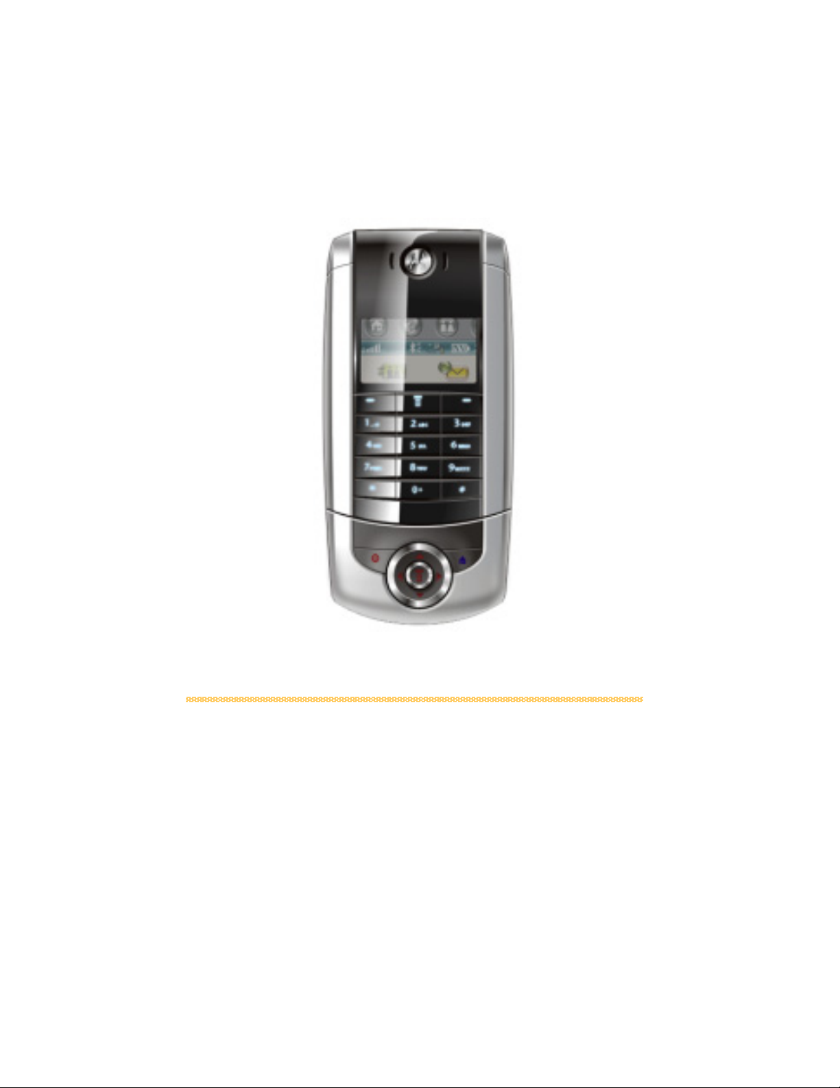
A780 Quad-Band EDGE / GPRS GSM Phone
Hardware INTERFACE DOCUMENT
Motorola, Inc.
Personal Communication Sector
Beijing Design Center
A780 Hardware Team
August 2nd, 2003
08/02/2003 Motorola Confidential Proprietary 1 / 126
Page 2

A780 Quad-Band Phone Hardware Interface Document Rev. 0.1
1. Revision History.......................................................................................................... 12
2. Purpose / Introduction................................................................................................ 13
3. PCAP2 Hardware Overview......................................................................................14
3.1 Power Management.............................................................................................. 15
3.1.1 Switching & Linear Regulators Default Configuration............................. 15
3.1.2 Regulator Usage Description ........................................................................ 16
1) V1 Linear Regulator....................................................................................... 16
2) V2 Linear Regulator....................................................................................... 16
3) V3 Linear Regulator....................................................................................... 16
4) V4 Linear Regulator....................................................................................... 16
5) V5 Linear Regulator....................................................................................... 16
6) V6 Linear Regulator....................................................................................... 17
7) V7 Linear Regulator....................................................................................... 17
8) V8 Linear Regulator....................................................................................... 17
9) V9 Linear Regulator....................................................................................... 17
10) V10 Linear Regulator................................................................................... 17
11) VAUX1 Linear Regulator............................................................................ 17
12) VAUX3 Linear Regulator............................................................................ 18
13) VAUX4 Linear Regulator............................................................................ 18
14) SW1 Switching Regulator............................................................................ 18
15) SW2 Switching Regulator............................................................................ 18
16) SW3 Switching Regulator............................................................................ 18
3.1.3 Power Distribution Tree................................................................................ 19
3.1.4 A780 Power Management Control............................................................... 21
3.2 A780 Audio System and PCAP2 Audio Section................................................. 26
3.2.1 A780 Audio System Architecture Block Diagram ...................................... 26
3.2.2 Audio Input Section....................................................................................... 28
3.2.3 Audio Output Section.................................................................................... 29
3.2.4 A780 Audio Routing and SPI Control ......................................................... 30
3.3 A/D Conversion And Channel Allocations......................................................... 31
3.3.1 Detailed Description Of Each A/D Channel................................................ 34
08/02/2003 Motorola Confidential Proprietary 2 / 126
Page 3

A780 Quad-Band Phone Hardware Interface Document Rev. 0.1
1) Li-Cell Battery A/D (AD1)............................................................................. 34
2) BATT_SENSE A/D (AD2) ............................................................................. 35
3) B+_SENSE A/D (AD3)...................................................................................35
4) MPB_SENSE A/D (AD4) ............................................................................... 35
5) BATT_THERM A/D (AD5)...........................................................................35
6) CHRG_ID (AD6) ............................................................................................ 37
7) Touch Panel AD (AD11 ~ AD14)................................................................... 37
3.3.2 A780 Charge Operation Description............................................................ 37
4. Neptune-LTE Logic Interfaces.................................................................................. 37
4.1 Neptune IC Description........................................................................................38
4.2 Neptune IC Features.............................................................................................38
4.3 Neptune Functional Summary............................................................................. 38
4.3.1 DSP.................................................................................................................. 38
1) DSP Memory................................................................................................... 39
2) SP BIST (DBIT).............................................................................................. 39
3) DSP Program Paging...................................................................................... 39
4) DSP Peripherals..............................................................................................40
5) Baseband Port Module (BBP) ....................................................................... 40
6) Layer1 Encryption Module (LEM)...............................................................40
7) DSP Timer Module (DTIMER).....................................................................40
8) Serial Audio CODEC Port (SAP).................................................................. 40
9) Direct Memory Access Controller (DMA) ................................................... 40
10) Viterbi Accelerator (VIAC)......................................................................... 40
11) DSP Special Interrupt Handler (DSIH)...................................................... 41
12) SP On Chip Emulator Debug Module (OnCE) ......................................... 41
13) DSP Debug Module (PDDM).......................................................................41
14) Voice CODEC (VOCOD)............................................................................. 41
15) DSP Clock Generator (DCLKG)................................................................. 42
16) IC Identification Module (IIM)................................................................... 42
17) Clock Monitor (CMON)............................................................................... 42
18) Power On Reset (POR)................................................................................. 42
08/02/2003 Motorola Confidential Proprietary 3 / 126
Page 4

A780 Quad-Band Phone Hardware Interface Document Rev. 0.1
19) System JTAG Controller (SJC)................................................................... 42
4.3.2 ARM7 MCU ................................................................................................... 43
4.3.2.1 MCU Memory ......................................................................................... 43
4.3.2.2 MCU Peripherals....................................................................................43
1) ARM7 Platform Core Arbiter (CARB).................................................... 43
2) ARM External Interface Module (AEIM)................................................ 43
3) ARM Peripheral Interface Gasket (APIG)..............................................44
4) ARM IPBus Interface (AIPI)..................................................................... 44
5) Alternate Master Arbiter (AMARB)........................................................ 44
6) Multiple Queue Serial Peripheral Interface (MQSPI)............................44
7) ARM7TDMI-S Interrupt Controller (AITC) .......................................... 44
8) SIM Interface Modifications (SIM) .......................................................... 44
9) Universal Asynchronous Receiver Transmitter (UART)........................ 45
10) Deep Sleep Module (DSM).......................................................................45
11) Watchdog Timer (WDOG)...................................................................... 45
12) General Packet Radio Service Encryption Module (GEM).................. 45
13) Keypad Port (KPP)................................................................................... 45
14) Enhanced General Purpose Timer (EGPT)........................................... 45
15) Test Control Module (TCM) ................................................................... 46
16) MCU Watchpoint (AWPT)......................................................................46
17) USB Digital Phase Locked Loop (REFPLL)..........................................46
18) Real Time Reference (RTR) .................................................................... 46
19) Real Time Clock (RTC) ........................................................................... 47
20) Display Memory Access Controller (DMAC)........................................47
21) Clock Control Module (CCM)................................................................. 47
22) External Interrupt Module (INT)........................................................... 47
23) Analog to Digital Interface (A2DIGL)....................................................47
4.3.3 Shared Peripherals......................................................................................... 48
4.3.3.1 Patch RAM (MXRAM) .......................................................................... 48
4.3.3.2 Universal Serial Bus Module (USB)...................................................... 48
4.3.3.3 General Purpose I/O (GPIO)................................................................. 48
08/02/2003 Motorola Confidential Proprietary 4 / 126
Page 5

A780 Quad-Band Phone Hardware Interface Document Rev. 0.1
4.3.3.4 MCU / DSP Interface (MDI)..................................................................48
4.3.3.5 Layer 1 Timer (L1T)............................................................................... 48
4.4 Neptune GPIO Summary..................................................................................... 49
4.5 Neptune-LTE Memory Interface......................................................................... 52
4.5.1 Flash................................................................................................................ 52
4.5.2 SRAM..............................................................................................................54
4.5.3 Neptune-LTE Chip Select Assignments....................................................... 54
4.6 Neptune MQSPI Module......................................................................................56
4.7 SIM Interface ........................................................................................................ 59
5. Neptune-LTE RF Interface........................................................................................62
5.1 RF6003 (Fractional-N RF Synthesizer) Chipset Description............................ 62
5.1.1 RF6003 Functional Description.................................................................... 62
5.1.2 RF6003 Serial Data Interface and Device Control ..................................... 63
5.2 RF2722 (GPRS / EDGE Receiver) Chipset Description.................................... 66
5.2.1 RF2722 Functional Description.................................................................... 66
5.2.2 RF2722 Serial Data Interface and Device Control ..................................... 67
5.3 RF3144 (Quad-Band Power Amplifier Module) Chipset Description............. 68
5.4 A780 RF System Signaling................................................................................... 69
5.4.1 RF System Block Diagram............................................................................ 69
5.4.2 Description of RF Signal and Interface ....................................................... 71
1) Antenna Switching Control........................................................................ 71
2) Digital RX Signal Interface........................................................................ 72
3) Digital TX Signal Interface........................................................................ 72
4) RF SPI Port Interface.................................................................................72
5) RF Control Related Signals........................................................................ 73
6) Neptune-LTE RF Related Signals............................................................. 74
6. AGPS Module Interface.............................................................................................75
6.1 AGPS Functional Block Diagram ....................................................................... 75
6.2 AGPS Interface Descriptions............................................................................... 75
6.2.1 AGPS_NRESET.............................................................................................76
6.2.2 UART Interface.............................................................................................. 76
08/02/2003 Motorola Confidential Proprietary 5 / 126
Page 6

A780 Quad-Band Phone Hardware Interface Document Rev. 0.1
6.2.3 Miscellaneous Signals .................................................................................... 77
6.2.4 AGPS Operation Mode Descriptions........................................................... 77
6.2.4.1 Boot Mode Operation............................................................................. 77
6.2.4.2 Tracking Mode Operation ..................................................................... 78
6.2.4.3 Sleep Mode Operation............................................................................ 78
6.3 AGPS Clock System.............................................................................................. 78
6.3.1 Reference Clock (24.5535MHz TCXO)........................................................ 78
6.3.2 RTC Clock (32.768KHz) ............................................................................... 78
6.4 AGPS Power On / Off Sequence.......................................................................... 78
7. Application Processor (Bulverde).............................................................................. 80
7.1 Bulverde Functional Overview............................................................................ 80
7.2 Bulverde Memory Interface.................................................................................82
7.2.1 Bulverde SDRAM Interface..........................................................................82
7.2.2 Bulverde Flash Interface............................................................................... 84
7.3 Bulverde GPIO Assignment................................................................................. 85
7.3.1 Bulverde GPIO Operation as Application-specific GPIO ......................... 85
7.3.2 Bulverde GPIO Operation as Alternate Function...................................... 87
7.3.3 Bulverde GPIO Operation as A780 Function ............................................. 91
7.4 A780 Keypad And Its Backlight Interface.......................................................... 95
7.4.1 Keypad Interface............................................................................................ 95
7.4.2 Keypad Backlight Interface.......................................................................... 99
7.5 A780 LCD Module Interface.............................................................................. 101
7.6 Bulverde Peripherals Interface.......................................................................... 108
7.6.1 Blue Tooth Module ...................................................................................... 109
7.6.2 Digital Camera............................................................................................. 110
TM
7.6.2.1 OmniVision
7.6.2.2 OmniVision
1.3MegaPixel Module Features................................ 111
TM
1.3MegaPixel Functional Description...................... 112
7.6.2.3 A780 Digital Camera Hardware Architecture................................... 113
7.6.2.4 A780 Digital Camera Operation Mode Description..........................115
7.6.3 Tri-Flash Card ............................................................................................. 116
8. A780 System Architecture Description...................................................................120
08/02/2003 Motorola Confidential Proprietary 6 / 126
Page 7

A780 Quad-Band Phone Hardware Interface Document Rev. 0.1
8.1 A780 System architecture block diagram.........................................................120
8.2 A780 Interconnection Link between Neptune-LTE & Bulverde (ICL).........121
8.3 A780 Clock System Control............................................................................... 123
8.3.1 Neptune-LTE Related Clock Signal........................................................... 123
8.3.2 RFMD Related Clock Signal....................................................................... 124
8.3.3 Bulverde Related Clock Signal................................................................... 124
8.3.4 Bluetooth Related Clock Signal.................................................................. 124
8.3.5 AGPS Related Clock Signal........................................................................ 125
8.3.6 PCAP2 Related Clock Signal...................................................................... 125
9. EMU Bus and A780 Accessories..............................................................................126
10. Reference Documentation List............................................................................... 126
08/02/2003 Motorola Confidential Proprietary 7 / 126
Page 8

A780 Quad-Band Phone Hardware Interface Document Rev. 0.1
List of Tables:
T
ABLE 1 - DEFAULT PCAP2 REGULATOR VOLTAGE AT PGM [1:0] SETTINGS ................. 15
ABLE 2 – PCAP2 SWITCHING MODE REGULATOR STANDBY CONTROL TRUE TABLE ..... 23
T
ABLE 3 – PCAP2 LINEAR MODE REGULATOR STANDBY CONTROL TRUE TABLE ........... 25
T
TABLE 4 –BULVERDE GPIO ASSIGNMENT FOR AUDIO SSP AND SPI ................................ 27
ABLE 5 – A780 A/D CONVERTER ALLOCATION TABLE .................................................. 34
T
ABLE 6 – BATTERY THERMISTOR READINGS OVER TEMPERATURE................................. 36
T
ABLE 7 – NEPTUNE DSP MEMORY REQUIREMENTS ........................................................ 39
T
ABLE 8 – NEPTUNE GPIO USAGE ASSIGNMENT (PA0 ~ PC7) ........................................ 50
T
TABLE 9 – NEPTUNE GPIO USAGE ASSIGNMENT (PC8 ~ PE15)....................................... 51
ABLE 10 – NEPTUNE-LTE CHIP SELECT ASSIGNMENT .................................................... 54
T
ABLE 11 – RF2722 REGISTER MAP ................................................................................. 57
T
ABLE 12 – RF6003 REGISTER MAP ................................................................................. 58
T
ABLE 13 – SIM CARD PRESENCE DETECT MATRIX ......................................................... 60
T
ABLE 14 – RF6003 SERIAL DATA INTERFACE REGISTER MAP ........................................ 65
T
ABLE 15 – RF2722 SERIAL DATA INTERFACE REGISTER MAP ........................................ 68
T
ABLE 16 – A780 ANTENNA SWITCH CONTROL TRUTH TABLE ........................................ 72
T
TABLE 17 – A780 RFMD CONTROL NEPTUNE-LTE GPIO ASSIGNMENT ........................ 74
ABLE 18 – A780 AGPS AND NEPTUNE-LTE CONNECTION ............................................ 76
T
ABLE 19 – MG4100 AGPS CHIPSET MODE SELECTION.................................................. 77
T
ABLE 20 – BULVERDE GPIO ALTERNATIVE FUNCTION (GPIO [0] ~ GPIO [20]) ........... 87
T
ABLE 21 – BULVERDE GPIO ALTERNATIVE FUNCTION (GPIO [21] ~ GPIO [60]) ......... 88
T
ABLE 22 – BULVERDE GPIO ALTERNATIVE FUNCTION (GPIO [61] ~ GPIO [100]) ....... 89
T
ABLE 23 – BULVERDE GPIO ALTERNATIVE FUNCTION (GPIO [101] ~ GPIO [120]) ..... 90
T
TABLE 24 – A780 BULVERDE GPIO ASSIGNMENT (GPIO [0] ~ GPIO [34]).................... 91
ABLE 25 – A780 BULVERDE GPIO ASSIGNMENT (GPIO [35] ~ GPIO [69]) .................. 92
T
ABLE 26 – A780 BULVERDE GPIO ASSIGNMENT (GPIO [70] ~ GPIO [104])................ 93
T
TABLE 27 – A780 BULVERDE GPIO ASSIGNMENT (GPIO [105] ~ GPIO [120]).............. 94
ABLE 28 – A780 MATRIX SCAN KEY ASSIGNMENT ........................................................ 96
T
TABLE 29 – A780 JOYSTICK SWITCH CONNECTION SCHEME ............................................ 97
08/02/2003 Motorola Confidential Proprietary 8 / 126
Page 9

A780 Quad-Band Phone Hardware Interface Document Rev. 0.1
T
ABLE 30 – A780 KEYPAD MATRIX SCAN TABLE ............................................................ 98
ABLE 31 – A780 BULVERDE GPIO ASSIGNMENT OF KEYPAD CONTROLLER .................. 98
T
ABLE 32 – PCAP2 BACKLIGHT DUTY CYCLE CONTROL BIT DEFINITION ..................... 100
T
TABLE 33 – A780 LCD POWER UP TIMING FIGURES....................................................... 103
ABLE 34 – A780 LCD POWER DOWN TIMING FIGURES ................................................ 104
T
ABLE 35 – A780 BULVERDE GPIO ASSIGNMENT OF LCD CONTROLLER ..................... 106
T
ABLE 36 – A780 LCD CONNECTOR PIN-OUT DEFINITION .............................................. 107
T
ABLE 37 – A780 DIGITAL CAMERA SIGNAL FUNCTION DESCRIPTION........................... 114
T
TABLE 38 – A780 DIGITAL CAMERA BULVERDE GPIO ASSIGNMENT ............................ 115
ABLE 39 – TRI-FLASH CARD PIN DEFINITION................................................................ 117
T
ABLE 40 – TRI-FLASH CARD MMC BUS AND SPI BUS COMPARISON ........................... 117
T
ABLE 41 – BULVERDE TRI-FLASH CARD GPIO ASSIGNMENT ....................................... 119
T
ABLE 42 – A780 ICL SIGNALS FUNCTION DESCRIPTION............................................... 122
T
ABLE 43 – BULVERDE 13MHZ CLOCK OUTPUT AT GPIO [9] SETTING BIT................... 124
T
08/02/2003 Motorola Confidential Proprietary 9 / 126
Page 10

A780 Quad-Band Phone Hardware Interface Document Rev. 0.1
List Of Figures
FIGURE 1 – A780 POWER DISTRIBUTION TREE DIAGRAM ............................................................................ 20
IGURE 2 – A780 POWER MANAGEMENT CONTROL DIAGRAM..................................................................... 21
F
F
IGURE 3 – A780 BULVERDE SLEEP AND OPERATION MODE POWER SUPPLY CONTROL.............................. 22
IGURE 4 – PCAP2 SWITCHING MODE REGULATOR STANDBY CONTROL .................................................... 23
F
F
IGURE 5 – PCAP2 LINEAR MODE REGULATOR STANDBY CONTROL .......................................................... 24
IGURE 6 – A780 AUDIO SYSTEM ARCHITECTURE BLOCK DIAGRAM........................................................... 26
F
F
IGURE 7 – PCAP2 AUDIO INPUT SECTION BLOCK DIAGRAM...................................................................... 28
IGURE 8 – PCAP2 AUDIO OUTPUT SECTION BLOCK DIAGRAM .................................................................. 29
F
F
IGURE 9 – A780 AUDIO ROUTING AND SPI CONTROL BLOCK DIAGRAM.................................................... 30
IGURE 10 – PCAP2 A/D CONVERSION TIMING DIAGRAM WITH AD_SEL = 0 ........................................... 31
F
F
IGURE 11 – PCAP2 A/D CONVERSION TIMING DIAGRAM WITH AD_SEL = 1 ........................................... 32
IGURE 12 – BATTERY THERMISTOR CONNECTION BLOCK DIAGRAM.......................................................... 36
F
F
IGURE 13 – A780 BASEBAND 64W18 + 8MB SRAM STACKED-CSP BLOCK DIAGRAM ........................... 52
IGURE 14 – A780 BASEBAND NEPTUNE-LTE AND MEMORY CONNECTION BLOCK DIAGRAM ................... 55
F
IGURE 15 – NEPTUNE MQSPI CONNECTION WITH PCAP2 AND RF6003 BLOCK DIAGRAM ....................... 57
F
IGURE 16 – A780 SIM CONNECTION BLOCK DIAGRAM.............................................................................. 59
F
IGURE 17 – A780 SIM PRESENT DETECTION CIRCUIT LOGIC BLOCK DIAGRAM ........................................ 60
F
IGURE 18 – R6003 FUNCTIONAL BLOCK DIAGRAM .................................................................................... 63
F
IGURE 19 – R6003 SERIAL DATA INTERFACE TIMING DIAGRAM ................................................................ 64
F
IGURE 20 – R6003 SERIAL DATA WRITE SEQUENCE (SINGLE ADDRESS) ................................................... 64
F
IGURE 21 – R6003 SERIAL DATA WRITE SEQUENCE (MULTIPLE ADDRESS)............................................... 64
F
IGURE 22 – R2722 FUNCTIONAL BLOCK DIAGRAM AND PIN OUT.............................................................. 67
F
IGURE 23 – R2722 SERIAL INTERFACE TIMING DIAGRAM .......................................................................... 68
F
F
IGURE 24 – A780 RFMD RF SYSTEM BLOCK DIAGRAM............................................................................ 70
IGURE 25 – A780 QUAD-BAND RF INTERFACE BETWEEN NEPTUNE, RF6003 & RF2722........................... 71
F
IGURE 26 – A780 AGPS FUNCTIONAL BLOCK DIAGRAM........................................................................... 75
F
IGURE 27 – A780 AGPS POWER ON AND OFF SEQUENCE .......................................................................... 79
F
IGURE 28 – BULVERDE PROCESSOR BLOCK DIAGRAM................................................................................ 81
F
IGURE 29 – BULVERDE MEMORY CONNECTION BLOCK DIAGRAM ............................................................. 83
F
IGURE 30 – BULVERDE GPIO PIN FUNCTION BLOCK DIAGRAM ................................................................. 86
F
IGURE 31 – A780 KEYPAD LOCATION DIAGRAM........................................................................................ 95
F
IGURE 32 – A780 KEYPAD INTERFACE BLOCK DIAGRAM........................................................................... 96
F
IGURE 33 – A780 JOYSTICK CONNECTION WITH BULVERDE KEYPAD CONTROL PIN ................................. 97
F
IGURE 34 – A780 JOYSTICK PIN CONNECTION DIAGRAM ........................................................................... 97
F
IGURE 35 – A780 KEYPAD BACKLIGHT CONTROL BLOCK DIAGRAM ......................................................... 99
F
IGURE 36 – A780 LCD MODULE ELECTRICAL BLOCK DIAGRAM ............................................................. 102
F
08/02/2003 Motorola Confidential Proprietary 10 / 126
Page 11

A780 Quad-Band Phone Hardware Interface Document Rev. 0.1
FIGURE 37 – A780 LCD MODULE HORIZONTAL READING / WRITING TIMING DIAGRAM .......................... 102
IGURE 38 – A780 LCD MODULE VERTICAL READING / WRITING TIMING DIAGRAM ............................... 103
F
F
IGURE 39 – A780 LCD POWER UP TIMING DIAGRAM .............................................................................. 103
IGURE 40 – A780 LCD POWER DOWN TIMING DIAGRAM ........................................................................ 104
F
F
IGURE 41 – A780 CONNECTION BLOCK DIAGRAM BETWEEN BULVERDE AND LCD MODULE ................. 105
IGURE 42 – A780 BULVERDE PERIPHERALS CONNECTIONS BLOCK DIAGRAM ......................................... 108
F
IGURE 43 – BCM2035 FUNCTIONAL BLOCK DIAGRAM ............................................................................ 110
F
IGURE 44 – OV9640 FUNCTIONAL BLOCK DIAGRAM ............................................................................... 112
F
IGURE 45 – A780 DIGITAL CAMERA SYSTEM ARCHITECTURE BLOCK DIAGRAM ..................................... 113
F
IGURE 46 – A780 DIGITAL CAMERA DETAILED CONNECTION WITH BULVERDE ...................................... 114
F
F
IGURE 47 – TRI-FLASH CARD OUTLINE DIAGRAM .................................................................................... 116
IGURE 48 – TRI-FLASH WITH MMC AND SPI INTERFACE BLOCK DIAGRAM............................................ 117
F
IGURE 49 – A780 TRI-FLASH CARD CONTROL BLOCK DIAGRAM ............................................................. 118
F
IGURE 50 – A780 QUAD-BAND SYSTEM ARCHITECTURE BLOCK DIAGRAM ............................................... 120
F
F
IGURE 51 – A780 QUAD-BAND INTERCONNECTION LINK BETWEEN NEPTUNE & BULVERDE ................... 121
IGURE 52 – A780 CLOCK SYSTEM CONTROL BLOCK DIAGRAM ............................................................... 123
F
IGURE 53 – PCAP2 CLOCK SELECTION OF VOICE PLL AND STEREO PLL BLOCK DIAGRAM .................. 125
F
08/02/2003 Motorola Confidential Proprietary 11 / 126
Page 12

A780 Quad-Band Phone Hardware Interface Document Rev. 0.1
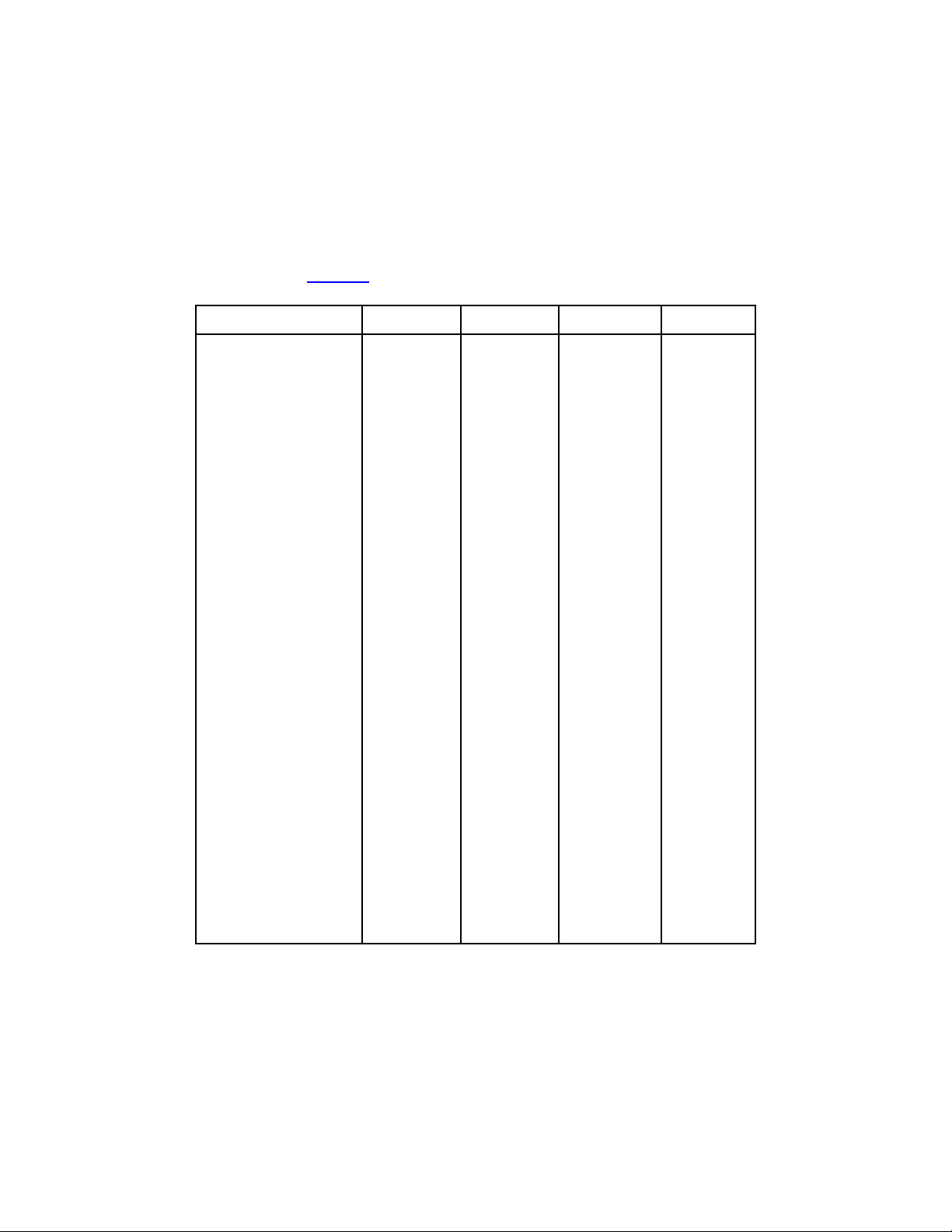
1. Revision History
Revision Date Section Author Reason
5. Neptune-LTE RF Interface
0.1 11/12/2003
6. AGPS Module Interface Cevin Wang
7.6.2 Digital Camera Cai Xiaochuan
Other Colin Li
Erin Geng
Initial Draft
08/02/2003 Motorola Confidential Proprietary 12 / 126
Page 13

A780 Quad-Band Phone Hardware Interface Document Rev. 0.1
2. Purpose / Introduction
The purpose of this document is to list and define the power supplies and interfaces
between base band and adjunct processor, base band and RF chipset etc for
GSM/DCS/CEL/PCS A780 cellular phone. This phone will bring to market with the
Neptune-LTE IC (base band call processor), Bulverde IC (adjunct application processor),
PCAP2 (Platform Audio Interface and Power Control) IC, as well as the air interface
RF6003 IC and RF3144 power amplifier IC. At the time of designing, the base band call
processor Neptune-LTE core will run at 1.8V while other IC will run at 2.775V. The
memory chipsets connected with Neptune-LTE need to run at 1.875V as well.
In this document, the major chipset features and functionality will be introduced as well
as the dedicated usage in A780 phone design. The interconnections between NeptuneLTE and Bulverde will be introduced in detail. The control signals from Neptune-LTE to
RF6003 and RF2722 will also introduced as well.
08/02/2003 Motorola Confidential Proprietary 13 / 126
Page 14

A780 Quad-Band Phone Hardware Interface Document Rev. 0.1
3. PCAP2 Hardware Overview
This section describes the general features of the PCAP2 (Platform
Control/Audio/Power) IC that will be developed for Dakota platform products. The
PCAP2 architecture is derived from previous devices such as GCAP-III and CCAP, with
feature enhancements as needed to support requirements of next-generation mobile
terminals.
The system-level requirements that have created the need for a new PCAP2 device
include the following:
Improved Power Cut/Power Power supply and control for external
Stereo Audio capability for Multimedia support
Dedicated Transceiver power supply
The PCAP2 will also include additional features to improve system efficiency
and reduce external component count such as:
Dual SPI control interface to allow access from two independent base band
processors
Multiple Switch mode power supply controllers for buck and/or boost
conversion
Additional independent, configurable voltage regulators
Enhanced touch screen interface
Improved backlight controller capability
Certain functions that were available on previous devices such as GCAP-II, GCAP-III
will NOT be carried over to the PCAP2 parts due to changes in system requirements or
lack of use on previous products.
These include:
Internal over voltage protection / clamp as implemented in CCAP
Negative voltage generation charge pump
Negative voltage linear regulators
DSC serial communication interface
08/02/2003 Motorola Confidential Proprietary 14 / 126
Page 15
A780 Quad-Band Phone Hardware Interface Document Rev. 0.1
3.1 Power Management
3.1.1 Switching & Linear Regulators Default Configuration
PGM0 & PGM1 along determine the power up default switching & linear
regulators’ voltage of PCAP2. Those two pins are also used to determine the
regulators turn on timing. The default voltage of each regulator at PGM [1:0]
settings is shown in Table 1
. A780 use PGM [1:0] = 0:1 as its default setting.
PGM [1:0] 00 01 10 11
V1
V2
V3
V4
V5
V6
V7
V8
V9
V10
SW1
SW2
SW3
SW4
VAUX1
VAUX2
VAUX3
VAUX4
VHOLD
VUSB
VUSB_MSTR
VSIM
VSIM2
V_VIB
1.600 2.775 1.875
2.775
1.875
2.775
1.275
2.775
1.875
1.875 2.775 1.875
2.775 2.775 2.775
2.775
1.875
1.875
2.475
5.000
2.250
1.600
5.500
2.775
2.775
1.275
1.575
5.000
1.200
1.875
5.500
2.775
1.875
1.875
2.475
5.000
2.250
1.600
5.500
2.775
2.775
1.550
2.775
2.775
2.775
2.775
1.875
1.575
5.000
1.600
1.875
5.500
OFF OFF OFF OFF
2.775
2.775
1.875
2.775
2.775
2.775
2.775
1.875
OFF OFF OFF OFF
OFF 3.0 OFF OFF
1.550
1.550
1.550
1.550
OFF OFF OFF OFF
OFF OFF OFF OFF
1.875
1.875
1.875
OFF
1.875 OFF
1.875 OFF
OFF OFF OFF OFF
Table 1 - Default PCAP2 Regulator Voltage at PGM [1:0] Settings
08/02/2003 Motorola Confidential Proprietary 15 / 126
Page 16

A780 Quad-Band Phone Hardware Interface Document Rev. 0.1
3.1.2 Regulator Usage Description
Regulators of PCAP2 were assigned as dedicated power supplies for Neptune-LTE or
Bulverde side. The functions were listed as below.
1) V1 Linear Regulator
V1 is a programmable linear regulator. It is programmable via the SPI bus to 1.275V ~
2.775V. For A780, V1 is programmed to 2.775V and is supplied directly by B+. This
regulator is on whenever the radio is turned on, and the initial power-up level is 2.775V
as default. V1 supplies Neptune-LTE interface control data pins, test pins and RF6003,
RF2722 SPI port. V1 is also used to provide I/O voltages to Bulverde sub-system. Some
external level shifters power supplies were also provided by V1. V1 was assigned as label
VAB_IO in A780 schematic.
2) V2 Linear Regulator
V2 is a programmable linear regulator. It is programmable via the SPI bus to 2.500V or
2.775V. For A780, V2 is programmed to 2.775V and is supplied directly by B+. This
regulator is on whenever the radio is turned on, and the initial power-up level is 2.775V
as default. V2 supplies Neptune internal CODEC circuitry power supply and PCAP2
internal audio related circuitry such as audio amplifiers, microphone bias etc. V2 was
assigned as label V_AUDIO in A780 schematic.
3) V3 Linear Regulator
V3 is a programmable linear regulator. It is programmable via the SPI bus to 1.075V ~
2.275V. For A780, V3 is programmed to 1.275V and is supplied directly by B+. This
regulator is on whenever the radio is turned on, and the initial power-up level is 1.275V
as default. V3 supplies the power for Bulverde VCC_SRAM power. V3 was assigned as
label VAP_SRAM in A780 schematic. This regulator can be switched off when Bulverde
entering into sleep mode, the control signal for this is PWR_EN of Bulverde.
4) V4 Linear Regulator
V4 is a programmable linear regulator. It is programmable via the SPI bus to 1.275V ~
2.775V. For A780, V4 is programmed to 2.775V as default. V4 supplies the power for
PCAP2 internal circuitry such as SPI module and RF related circuitry etc. V4 was
assigned as VRF_VCO in A780 schematic. During standby mode of Neptune-LTE
system, V4 should be switch off when Standby pin of PCAP2 asserted.
5) V5 Linear Regulator
V5 is a programmable linear regulator. It is programmable via the SPI bus to 1.275V ~
2.775V. For A780, V5 is programmed to 2.775V as default. V5 supplies the power for
PCAP2 internal circuitry such as SPI module and RF related circuitry etc. V5 was
08/02/2003 Motorola Confidential Proprietary 16 / 126
Page 17

A780 Quad-Band Phone Hardware Interface Document Rev. 0.1
assigned as VRF_LNA in A780 schematic. During standby mode of Neptune-LTE
system, V5 should be switch off when Standby pin of PCAP2 asserted.
6) V6 Linear Regulator
V6 is a programmable linear regulator. It is programmable via the SPI bus to 2.475V or
2.775V. For A780, V6 is not used.
7) V7 Linear Regulator
V7 is a programmable linear regulator. It is programmable via the SPI bus to 1.875V or
2.775V. For A780, V7 is programmed to 2.775V and is supplied directly by B+. This
regulator is on whenever the radio is turned on, and the initial power-up level is 2.775V
as default. V7 supplies to Neptune-LTE, RF6003 & RF2722 RF related circuitries. V7
was assigned as label VRF_TXRX in A780 schematic.
8) V8 Linear Regulator
V8 is a programmable linear regulator. It is programmable via the SPI bus to 1.075V ~
2.275V. For A780, V8 is programmed to 1.275V and is supplied directly by B+. This
regulator is on whenever the radio is turned on, and the initial power-up level is 1.275V
as default. V8 supplies the power for Bulverde VCC_PLL power. V8 was assigned as
label VAP_PLL in A780 schematic. This regulator can be switched off when Bulverde
entering into sleep mode, the control signal for this is PWR_EN of Bulverde.
9) V9 Linear Regulator
V9 is a programmable linear regulator. It is programmable via the SPI bus to 1.575V ~
2.775V. For A780, V9 is programmed to 1.575V and is supplied directly by B+. This
regulator is on whenever the radio is turned on, and the initial power-up level is 1.575V
as default. V9 supplies to Neptune LVDD1 as Neptune internal reference voltage. V9
was assigned as label VBB_REF in A780 schematic. This power supply is also connected
with PCAP2 VCC_OUT pin to provide power for PCAP2 internal 32KHz oscillator and
output buffer.
10) V10 Linear Regulator
V10 is an un-programmable linear regulator for its output voltage, but it can be switched
on or off via the SPI port. V10 output at 5.0V and is supplied by SW3. This regulator is
on whenever the radio is turned on, and the initial power-up level is 5.0V as default. V10
is not used in A780 design.
11) VAUX1 Linear Regulator
VAUX1 is a programmable linear regulator. It is programmable via the SPI bus to
1.275V ~ 2.775V. For A780, VAUX1 is programmed to 1.875V and is supplied directly
08/02/2003 Motorola Confidential Proprietary 17 / 126
Page 18

A780 Quad-Band Phone Hardware Interface Document Rev. 0.1
by B+. This regulator is on whenever the radio is turned on, and the initial power-up level
is 1.875V as default. VAUX1 supplies Bluetooth core and RF power. VAUX1 was
assigned as label VBT_RF in A780 schematic.
12) VAUX3 Linear Regulator
VAUX1 is a programmable linear regulator. It is programmable via the SPI bus to
1.275V ~ 2.775V. For A780, VAUX1 is programmed to 2.800V and is supplied directly
by B+. This regulator is off when the radio is turned on, and the initial power-up level is
0V as default. VAUX3 supplies power to Tri-Flash card. VAUX3 was assigned as label
VAP_MMC in A780 schematic.
13) VAUX4 Linear Regulator
VAUX4 is a programmable linear regulator. It is programmable via the SPI bus to
1.800V ~ 5.000V. For A780, VAUX4 is programmed to 3.000V and is supplied directly
by B+. This regulator is on whenever the radio is turned on, and the initial power-up level
is 3.00V as default. VAUX4 supplies power to AGPS RF module. VAUX4 was assigned
as label VAP_GAM_RF in A780 schematic.
14) SW1 Switching Regulator
SW1 is a programmable switching regulator. It is programmable via the SPI bus to
0.900V ~ 2.250V. For A780, SW1 is programmed to 1.2V and is supplied directly by B+.
This regulator is on whenever the radio is turned on, and the initial power-up level is
1.20V as default. SW1 supplies power to Bulverde VCC_CORE domain. SW1 was
assigned as label VAP_CORE in A780 schematic.
15) SW2 Switching Regulator
SW2 is a programmable switching regulator. It is programmable via the SPI bus to
0.900V ~ 2.250V. For A780, SW2 is programmed to 1.875V and is supplied directly by
B+. This regulator is on whenever the radio is turned on, and the initial power-up level is
1.875V as default. SW2 supplies power to Bulverde memory system and Neptune-LTE
memory interface. SW1 was assigned as label VAB_MEM in A780 schematic.
16) SW3 Switching Regulator
SW3 is a programmable switching regulator. It is programmable via the SPI bus to 4.00V
~ 5.50V. For A780, SW3 is programmed to 5.5V as default and is supplied directly by
B+. This regulator is on whenever the radio is turned on, and the initial power-up level is
5.50V as default. SW3 supplies power to PCAP2 VBUS_IN as USB OTG host function.
SW3 was assigned as label V_BOOST in A780 schematic.
08/02/2003 Motorola Confidential Proprietary 18 / 126
Page 19

A780 Quad-Band Phone Hardware Interface Document Rev. 0.1
3.1.3 Power Distribution Tree
For A780 cellular phone, not all the regulators listed in Table 1
A780 power distribution tree in which all the used regulators load were addressed.
PCAP2 provides all the regulated power supplies to Neptune-LTE subsystem, Bulverde
adjunct processor sub-system, Bluetooth system and AGPS system etc.
are used. Figure 1 shows
08/02/2003 Motorola Confidential Proprietary 19 / 126
Page 20
A780 Quad-Band Phone Hardware Interface Document Rev. 0.1
_
_
RF3144
VBATT
PCAP2
V5 (Linear)
VRF_LNA
(2.775V)
RF6003
VDD_RX
RF2722
FLT_VCC
LNA_VCC
Neptune
BVDD
CVDD1
CVDD2
CVDD3
DVDD
EVDD
JVDD
VDDA
Bulverde
VCC_IO
VCC_BB
Hall Effect
Supply
LCD
Module
V
PCAP2
V4 (Linear)
VRF_VCO
(2.775V)
RF6003
VCCV
RF2722
MIX_VCC
LO_VCC
VCO
PCAP2
V1 (Linear)
VAB_IO
(2.775V)
PCAP2
PRISSIVCC
SECSSIVCC
PRISPIVCC
SECSPIVCC
USBDIGVCC
Blue-Tooth
V-I-O
Digital Camera
LCD Module
VDD2
LED
VCC
VCC
VDD1
Single Cell Li-Ion
B+
PCAP2
PCAP2
ALRT_VCC
V9 (Linear)
VBB_REF
(1.575V)
Neptune
LVDD1
PCAP2
SW3 (Boost)
V_BOOST
(5.50V)
PCAP2
IN
VUSB
PCAP2
SW1 (BUCK)
VAP_CORE
(0.9 ~ 1.3V)
Bulverde
VCC_CORE
PCAP2
AGPS
VDD_IO
Other
U602
U604
U605
U606
U401
V7 (Linear)
VRF_TXRX
(2.775V)
Neptune
VDD_TXRX
RF6003
VCC (_PLL)
VDD
RF2722
DIG_VCC
PCAP2
VAUX1 (Linear)
VBT_RF
(1.875V)
Blue-Tooth
BTRF_REG
AGPS
VAP_GAM_RF
PCAP2
VUSB (Linear)
VAP_USB
(3.3V)
Bulverde
VCC_USB
PCAP2
VAUX3 (Linear)
VAP_MMC
(2.80V)
MMC / SD Card
MMC_VCC
PCAP2
VAUX4 (Linear)
VAP_GAM_RF
(3.00V)
AGPS
VGAM_RF
PCAP2
V8
(Linear)
VAP_PLL
(1.275V)
Bulverde
VCC_PLL
PCAP2
SW2 (BUCK)
VAB_MEM
(1.875V)
Neptune
QVDD
Stack-Memory
VCC1
VCC2
VCCQ
S-VCC
VPP
Bulverde
VCC_MEM
PCAP2
V3 (Linear)
VAP_SRAM
(1.275V)
Bulverde
VCC_SRAM
PCAP2
LEDG
LEDR
PCAP2
(Linear)
SIM_VCC
(1.875V/3.0V)
Neptune
SIM Card
RRight Amplifier
VSIM
FVDD
VCC
PCAP2
V2 (Linear)
V_AUDIO
(2.775V)
Neptune
VDD_CODEC
PCAP2
A1 Amplifier
A4 Amplifier
Left PGA
Right PGA
ALeft Amplifier
Phone DAC
Stereo DAC
A3 Amplifier
A5 Amplifier
MIC_BIAS1
MIC_BIAS2
PCAP2
V_VIB
(Linear)
VVIBB
(1.30V)
Vibrator
POS
Figure 1 – A780 Power Distribution Tree Diagram
08/02/2003 Motorola Confidential Proprietary 20 / 126
Page 21

A780 Quad-Band Phone Hardware Interface Document Rev. 0.1
T
I/Q
VCO1
VCO2
3.1.4 A780 Power Management Control
Figure 2
shows the detailed control signal connection for power management in A780.
Bulverde
VCC_CORE
VCC_MEM
VCC_PLL
USB Host Port3
GPIO [89]
PWR_EN
VCC_IO etc
VCC_SRAM
GPIO [1]
ICL
TC_MM_EN
nPWR_EN
USB
INT3
INT0
BVDD
Neptune
VDD_CODEC
STANDBY
SPI_CS3
BB_SPI
LVDD1
QVDD
BB_TX
BB_RX
L1_Timer
RF_SPI
RF_SPI
VBB_IO
VA
VAP_PLL
VAP_SRAM
VAB_MEM
P_CO
RE
VAB_IO
PCAP2_SEC_IN
SEC_SPI
PRI_SPI
PCAP2_PRI_IN
STANDBY
V_AUDIO
VBB_REF
VBB_CORE
BT
DC
INT
V1
V3
V8
SW1
SW2
SEC_SPI
Controllable
VAUX1
VAUX4
STANDBY2
V1
INTPRI
STANDBY
PRI_SPI
PCAP2
V2
SW2
CHAGC
V9
V10_IN
MAIN_FE
VCC_OUT
SW3
Boost
B+
Hall-Effect
USB
AGPS
EMU Support
EXT_B+
Mini-USB Connector
RAW_EXT_B+
LCD Module
Figure 2 – A780 Power Management Control Diagram
In Figure 2
, A780 power management block diagram, the power saving mode of
operation for both Neptune-LTE baseband and Bulverde adjunct processor need to be
described as below.
RF6003
RF2722
SAW
RF Switch
BATT+
V
V
Range
RAMP
RF3144
GSM/DCS
CEL/PCS
08/02/2003 Motorola Confidential Proprietary 21 / 126
Page 22
A780 Quad-Band Phone Hardware Interface Document Rev. 0.1
There are two standby control signals with PCAP2 in which is different from PCAP2
design. In A780 power management design, one standby control pin of PCAP2 is
connected with Neptune-LTE standby pin and another standby control pin is connected
with Bulverde PWR_EN pin (need to be inverted as PCAP2 required).
During the period of Neptune-LTE in standby mode, Neptune-LTE asserts it’s
STANDBY pin and PCAP2 shutdown the power supplies to Neptune-LTE subsystem
needed to be for power saving purpose. The power supplies need to be switched off for
Neptune-LTE standby mode is V7, V4 & V5.
In A780 adjunct processor power saving mode, Bulverde needs to enter into Sleep mode
for achieving minimum power consumption. That needs the power supplies provided to
Bulverde Core, PLL and internal SRAM power domain to be switched off after Bulverde
entered into sleep mode. The pin PWR_EN of Bulverde will be changed from logic
HIGH to logic LOW after Bulverde entering into Sleep mode. The inverted PWR_EN
(nPWR_EN) was connected with PCAP2 STANDBY2 pin in A780, so when
STANDBY2 of PCAP2 was changed from logic LOW to logic HIGH, the power supplies
to Bulverde Core, PLL and internal SRAM can be shutdown. Two types of power
supplies involved into Bulverde sleep mode operation, one is a linear regulator and
another one is switching mode regulator.
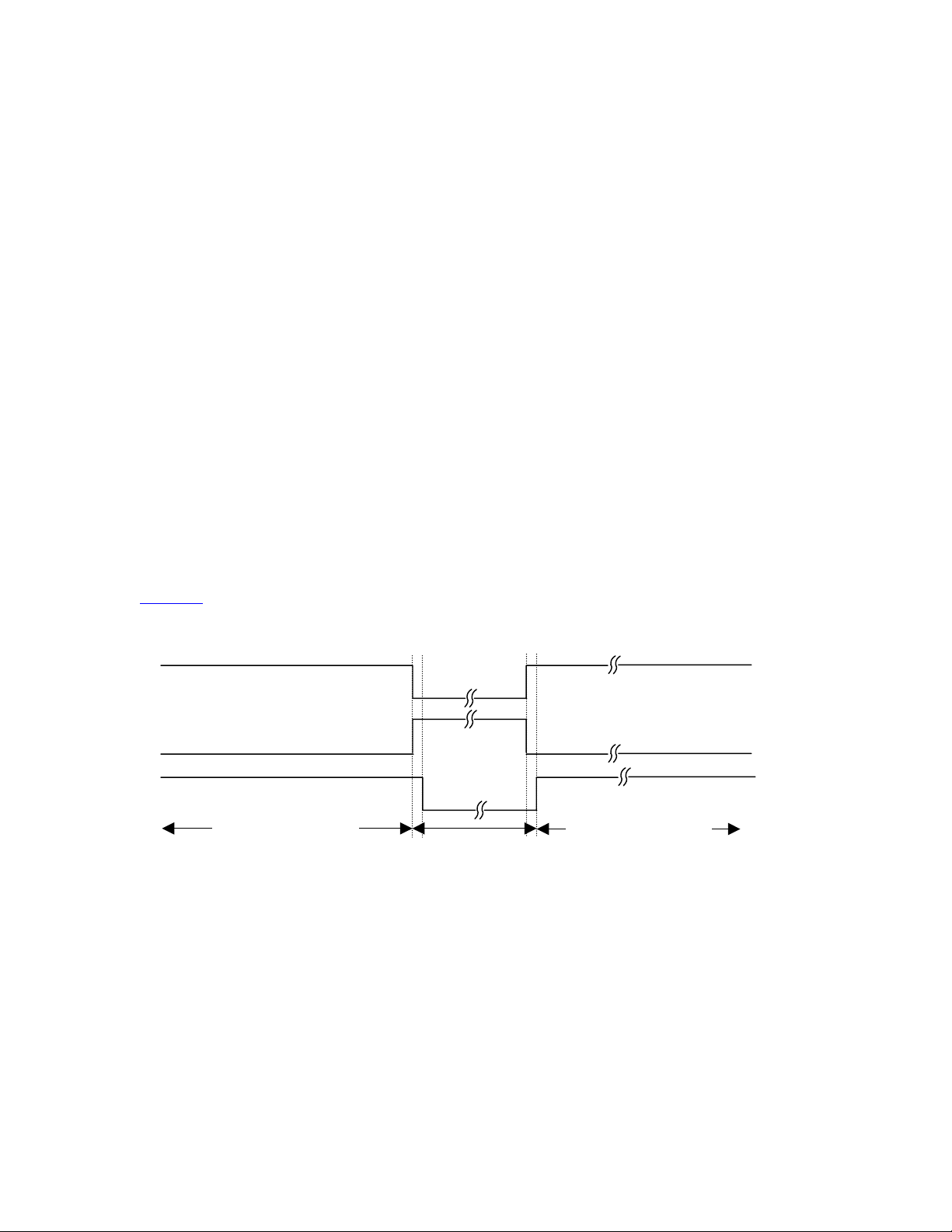
Figure 3
illustrates the waveform of control sequence for VCC_SRAM, VCC_PLL, and
VCC_CORE with PWR_EN.
PWR_EN
STANDBY2 (nPWR_EN)
SW1, V3, V8 (CORE, SRAM, PLL)
Running Mode Period
Sleep Mode Period
Running Mode Period
Figure 3 – A780 Bulverde Sleep and Operation Mode Power Supply Control
The state of PWR_EN signal of Bulverde will change from high to low automatically
after software entering into sleep mode and can automatically change back to high from
low while triggered by wakeup events settled by software. There is a small delay for
SW1, V3 and V8 to setup after STANDBY2 pin changed from high to low. But that is
within the timing requirement of Bulverde.
08/02/2003 Motorola Confidential Proprietary 22 / 126
Page 23
A780 Quad-Band Phone Hardware Interface Document Rev. 0.1
)
])
)
[
])
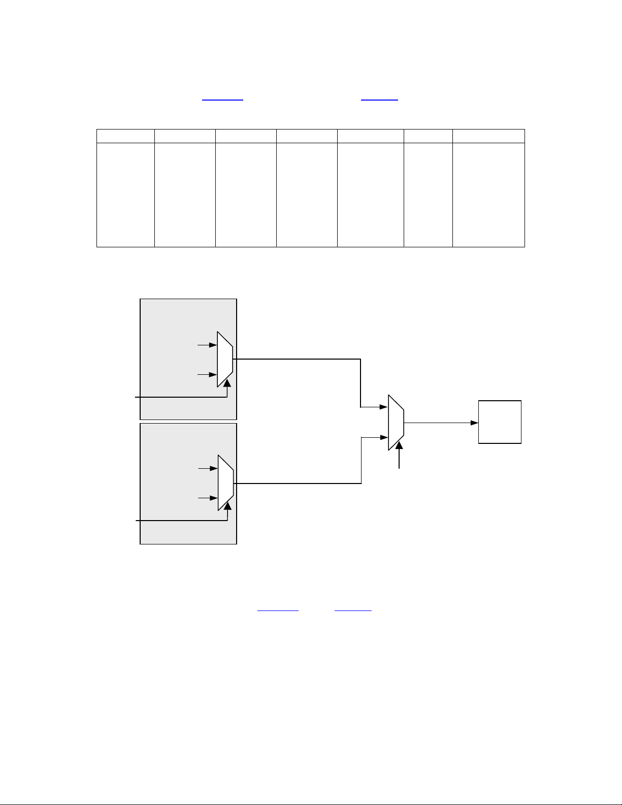
For switching mode regulator standby operation in PCAP2 (SW1 was used in A780), the
control block diagram Figure 4
and control True Table Table 2 can be applied for this
kind of operation.
SWx_MODE11 SWx_MODE10 SWx_MODE01 SWx_MODE00 STANDBYy Pin Mode Voltage
X X 0 0 0 OFF 0
X X 0 1 0 Sync SWx [3:0]
X X 1 0 0 Nonsync SWx [3:0]
X X 1 1 0 Low Power
0 0 X X 1 OFF 0
0 1 X X 1 Sync SWx_DVS [3:0]
1 0 X X 1 Nonsync SWx_DVS [3:0]
1 1 X X 1 Low Power SWx_DVS [3:0]
Table 2 – PCAP2 Switching Mode Regulator Standby Control True Table
Primary SPI
STANDBY1
SWx_MODE1 [1:0]
SWx [3:0]_DVS
SWx_MODE0 [1:0]
SWx [3:0
Secondary SPI
(SWx_MODE_PRI [1:0], SWx_PRI [3:0])
(SWx_MODE [1:0],
SWx_VOLTSEL [3:0])
SWx
Switching
Regulator
STANDBY2
SWx_MODE1 [1:0]
SWx [3:0]_DVS
SWx_MODE0 [1:0]
SWx
3:0
(SWx_MODE_PRI [1:0], SWx_SEC [3:0])
(In Primary VREG_MASK Register)
SWx_SEL
Figure 4 – PCAP2 Switching Mode Regulator Standby Control
There are several items of note in Figure 4
and in Table 2. First is the fact that either SW1
or SW2 can be controlled by either the primary or secondary SPI. For switching mode
regulators control, no OR gate was put into PCAP2 control. This is controlled by the
SW1_SEL and SW2_SEL bits in the VREG_MASK register. Furthermore, either
switcher can be placed in any of the four possible switcher modes arbitrarily, based on
the state of the STANDBY pins (the STANDBY1 pin controls the primary SPI
regulator(s), where as the STANDBY2 pin controls the secondary SPI regulator(s).
Finally, the switching regulator mode control design allows the system to dynamically
change the output voltage of each switcher based on the STANDBY pins.
08/02/2003 Motorola Confidential Proprietary 23 / 126
Page 24
A780 Quad-Band Phone Hardware Interface Document Rev. 0.1
Bulverde internal SRAM and PLL power domain, VCC_SRAM and VCC_PLL
respectively, are linear regulators provided by PCAP2. VCC_SRAM power supply is
provided by PCAP2 V3 and VCC_PLL power supply is provided by PCAP2 V8 in A780
power management design. During sleep mode of Bulverde, V3 and V8 needs to be
shutdown for achieving minimum power consumption.
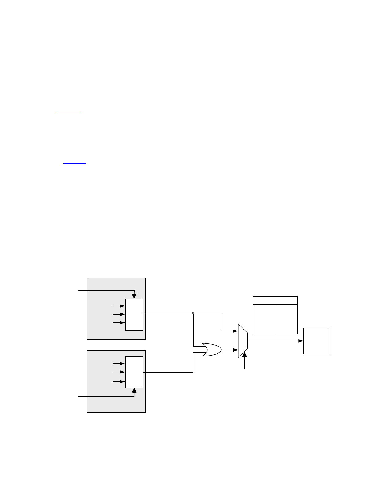
Figure 5
shows a block diagram of standby control for those linear regulators (includes
V3 and V8, but not limited to them in PCAP2) that have standby controllability. Each
linear regulator is controlled via SPI bits in both the primary and secondary SPIs. Mode
decoder logic in each SPI block combines these SPI bits with the STANDBY pins
(STANDBY1 for primary, STANDBY2 for secondary), and outputs Vx_MODE_PRI
[1:0] and Vx_MODE_SEC [1:0]. The truth table for the mode decoder logic is shown
in Table 3
. Note that not all regulators have corresponding EN bits in the secondary SPI.
In these cases, the secondary EN bit is assumed to be a logic 1. when interpreting the
truth table. The regulators that cannot be controlled via STANDBY1 or STANDBY2
are: VSIM, VSIM2, TS_REF, VHOLD, V_VIB, and VFLASH. Some of these regulators
can be placed in a low power mode (VSIM, VSIM2, TS_REF, and VHOLD), but the low
power feature is independent of standby control in that case.
One noteworthy feature of the linear regulator standby control scheme is the mode
OR.ing function. This function simply selects the highest power mode between
Vx_MODE_PRI [1:0] and Vx_MODE_SEC [1:0]. This function can be disabled via the
Vx_SEL bits in the VREG_MASK register. This register is only accessible by the
primary SPI port, and is used by the primary SPI to allow or disallow control from the
secondary SPI port of any set of individual regulators.
STA
NDBY1
Primary SPI
Vx_EN
Vx_LOWPWR
Vx_STDY
Mode
Encoder
Vx_MODE_PRI [1:0]
MODE [1:0] Mode
00 OFF
01 Not Used
10 Low Power
11 ON
Vx_MODE[1:0]
Vx
Regulator
Vx_EN
Vx_LOWPWR
Vx_STDY
Mode
Encoder
Vx_MODE_SEC [1:0]
(In Primary VREG_MASK Register)
Vx_SEL
NDBY2
STA
Secondary SPI
Figure 5 – PCAP2 Linear Mode Regulator Standby Control
08/02/2003 Motorola Confidential Proprietary 24 / 126
Page 25

A780 Quad-Band Phone Hardware Interface Document Rev. 0.1
EN bit STBY bit LOWPWR bit STANDBYy Pin Mode Vx_MODE_PRI/SEC [1:0]
0 X X X OFF 00
1 0 0 0 ON 11
1 0 0 1 ON 11
1 0 1 0 Low Power 10
1 0 1 1 Low Power 10
1 1 0 0 ON 11
1 1 0 1 OFF 00
1 1 1 0 ON 11
1 1 1 1 Low Power 10
Table 3 – PCAP2 Linear Mode Regulator Standby Control True Table
To switch off V3 (VCC_SRAM) and V8 (VCC_PLL) when STANDBY2 asserted,
V3_EN and V8_EN need to be clear by primary SPI since those two bits are accessible
only by primary SPI. In A780 design, the primary SPI port of PCAP2 is connected with
Neptune-LTE. So Neptune-LTE software should clear V3_EN and V8_EN after booting
up.
08/02/2003 Motorola Confidential Proprietary 25 / 126
Page 26

A780 Quad-Band Phone Hardware Interface Document Rev. 0.1
K
K
SSP
2
K
t
K
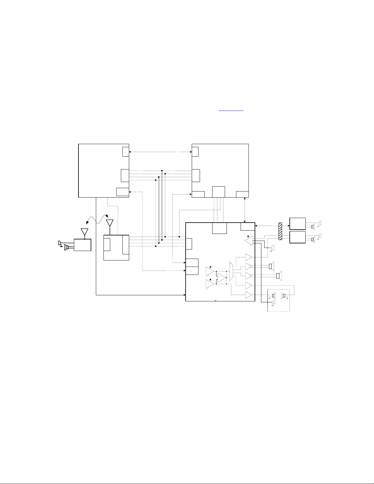
3.2 A780 Audio System and PCAP2 Audio Section
3.2.1 A780 Audio System Architecture Block Diagram
A780 phone design supports the voice audio, stereo audio and Bluetooth audio in its
audio system architecture illustrated in Figure 6
illustrated in Figure 6
.
. The SPI port to PCAP2 control is also
Bulverde
-
GPIO [88]
GPIO [38]
GPIO [37]
GPIO [22]
SAP_TXD
SAP_RXD
SAP_FRM
SAP_CLK
SAP_TXD
SAP_RXD
SAP_FRM
SAP_CL
STDA
Neptune-LTE
SRDA
SC2A
SCKA
GPIO [29]
SSP-1
GPIO [25]
GPIO [24]
GPIO [26]
GPIO [52]
SSP-3
GPIO [89]
GPIO [81]
GPIO [83]
AP_SPI_FRM
AP_SPI_CLK
AP_SPI_TXD
AP_SPI_RXD
AP_SPI_CS
AP_AUD_CLK
AP_AUD_TXD
AP_AUD_FRM
SAP_CL
SAP_TXD
SAP_FRM
SAP TXD
SAP FRM
SAP CL
SAP RXD
SEC_MOSI
SEC_CE
SEC_MISO
TX
BITCLK1
RX1
FSYNC1
RX0
FSYNC0
BITCLK0
SEC_SPI_CLK
ASAP TXD
ASAP FS
ASAP CL
ASAP RXD
PCAP2-II
Blue-Tooth
Figure 6 – A780 Audio System Architecture Block Diagram
The alternate functions of Bulverde GPIO assignment for audio and SPI settings shows in
Table 4
.
BT
Headse
08/02/2003 Motorola Confidential Proprietary 26 / 126
Page 27

A780 Quad-Band Phone Hardware Interface Document Rev. 0.1
A780 Function
AP SPI - AP_SPI_CLK GPIO[29]
AP SPI - AP_SPI_FRM GPIO[24]
AP SPI - AP_SPI_RXD GPIO[26]
AP SPI - AP_SPI_TXD GPIO[25]
SAP Codec - SAP_CLK GPIO[22]
SAP Codec - SAP_FRM GPIO[37]
SAP Codec - SAP_RXD GPIO[38]
SAP Codec - SAP_TXD GPIO[88]
Stereo Codec - AP_AUD_CLK GPIO[52]
Stereo Codec - AP_AUD_FRM GPIO[83]
Stereo Codec - AP_AUD_RXD GPIO[89]
Stereo Codec - AP_AUD_TXD GPIO[81]
GPIO
Table 4 –Bulverde GPIO Assignment for Audio SSP and SPI
Alternative Input Alternative Output
[ 01 ] [ 10 ] [ 11 ] [ 01 ] [ 10 ] [ 11 ]
AC97_SDATA_IN_0 I2S_SDATA_IN SSPSCLK SSPRXD2 SSPSCLK
CIF_FV SSPSFRM CIF_FV SSPSFRM
SSPRXD CIF_PCLK
CIF_LV CIF_LV SSPTXD
SSPEXTCLK2 SSPSCLK2EN SSPSCLK2 KP_MKOUT[7] SSPSYSCLK2 SSPSCLK2
FFDSR SSPSFRM2 KP_MKIN[3] USB_P2_8 SSPSFRM2 FFTXD
FFRI KP_MKIN[4] USB_P2_3 SSPTXD3 SSPTXD2 PWM_OUT[1]
USBHPWR[0] SSPRXD2 SSPSFRM2 SSPSFRM2
CIF_DD[4] SSPSCLK3 BB_OB_CLK SSPSCLK3
SSPSFRM3 BB_IB_CLK CIF_DD[4] SSPSFRM3
SSPRXD3 AC97_SYSCLK USBHPEN[0] SSPTXD2
CIF_DD[0] SSPTXD3 BB_OB_DAT[0]
08/02/2003 Motorola Confidential Proprietary 27 / 126
Page 28
A780 Quad-Band Phone Hardware Interface Document Rev. 0.1
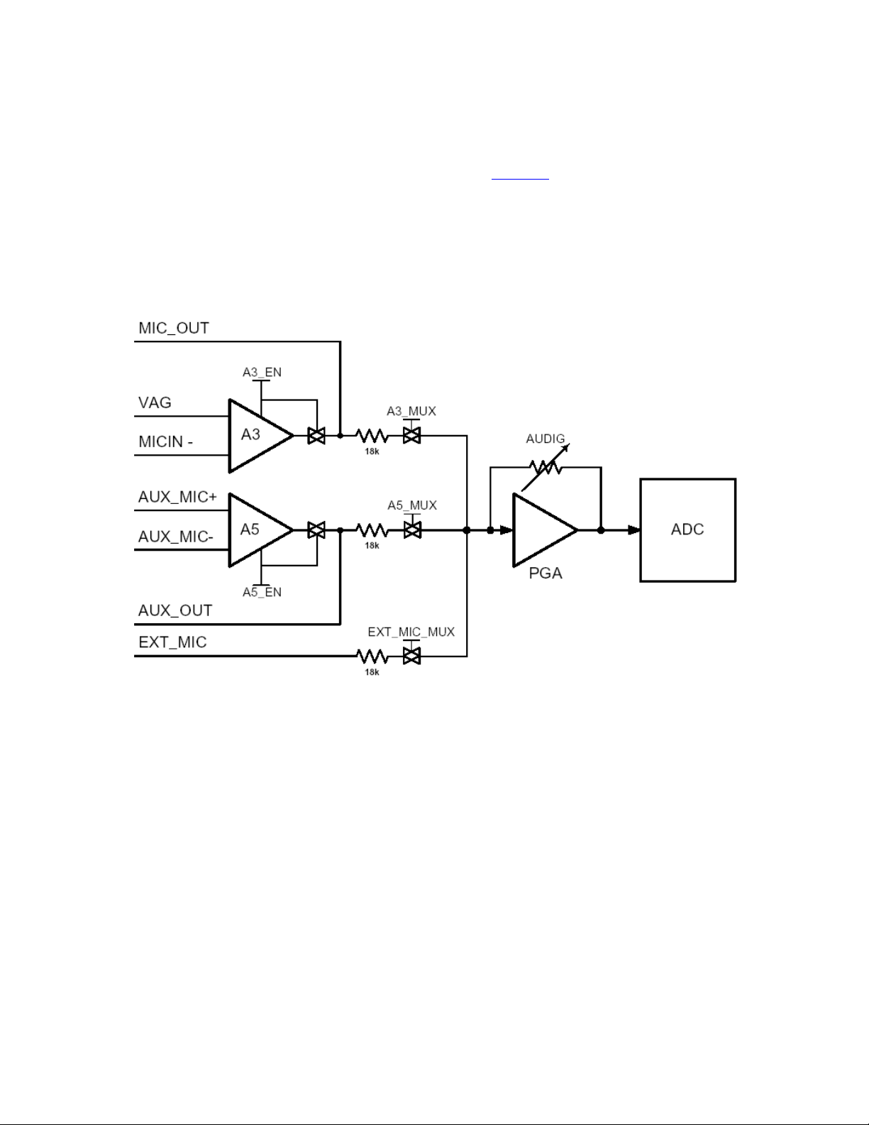
3.2.2 Audio Input Section
PCAP2 Audio Input Section block diagram shows in Figure 7
. Any one of three
equivalent microphone inputs can be selected. These inputs are EXT_MIC, the output of
the differential input microphone amplifier A3 or the output of the differential auxiliary
microphone amplifier, A5. These three inputs are single ended with respect to VAG
(Note: AUX_MIC+ should be DC connected to VAG to avoid an offset relative to the
A/D input). MIC_BIAS is derived from VAG for best noise performance. MB_CAP
bypasses the gain from VAG to MIC_BIAS to keep the noise balanced.
Figure 7 – PCAP2 Audio Input Section Block Diagram
Following the input stage and multiplexer is a selectable gain stage and 30kHz low-pass
anti-aliasing filter. This low-pass filter may be designed to whatever order is needed to
insure that aliased components are not present in the output. The gain of the selectable
gain stage can be selected in 1dB steps from 0dB to +31dB.
Depending on the design of the A/D converter the output of the anti-aliasing filter may be
clamped to keep from overdriving the A/D converter.
The audio input bits control the configuration of the input. These bits select the gain,
enable or disable the input, select between the EXT_MIC, A5 amplifier output, or A3
amplifier output, and select or deselect the CODEC’s high pass input filter. Also, these
bits can select a loop-back mode that takes the digital output of the input A/D converter,
and loops it directly back to the D/A output section for testing.
08/02/2003 Motorola Confidential Proprietary 28 / 126
Page 29
A780 Quad-Band Phone Hardware Interface Document Rev. 0.1
The switch shown between A3 output and MIC_OUT and the switch shown between A5
output and AUX_OUT are conceptual. It is possible that the amplifier will be high
impedance when in its powered down state.
3.2.3 Audio Output Section
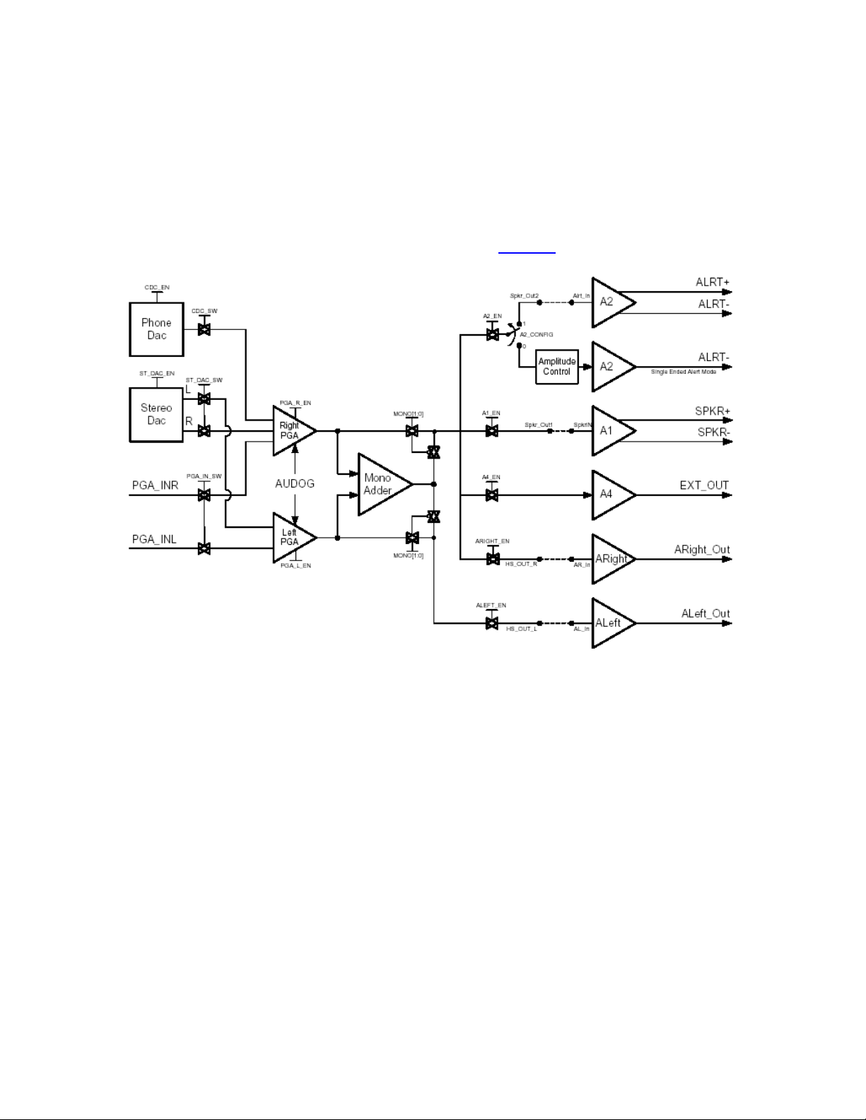
PCAP2 Audio Output section block diagram shows in Figure 8
.
Figure 8 – PCAP2 Audio Output Section Block Diagram
It shows that the audio out of the telephone CODEC or the right channel of the stereo
DAC can be routed via the right PGA to any one of four outputs. These outputs are: the
internal earpiece speaker amplifier, A1, the alert amplifier, A2, the external speaker
amplifier, A4, or the dedicated headset right channel speaker amplifier, ARight. All of
these outputs can be simultaneously connected to the right PGA so care should be taken
not enable multiple amplifiers at the same time if this is not desired.
The Mono adder can be used to sum the left and right channels of the stereo DAC or
signals supplied to the left and right PGA inputs. The Mono adder can then attenuate the
summed signals by 0dB, 3dB or 6dB and an identical monophonic signal to any of output
amplifiers mentioned above.
SPKR_OUT1, SPKR_OUT2, HS_OUT_R and HS_OUT_L should maintain their DC
levels even when not selected or if the audio is off.
08/02/2003 Motorola Confidential Proprietary 29 / 126
Page 30
A780 Quad-Band Phone Hardware Interface Document Rev. 0.1
SPKR_OUT1, SPKR_OUT2, HS_OUT_R, HS_OUT_L, PGA_INR, and PGA_INL are
all capacitor coupled.
3.2.4 A780 Audio Routing and SPI Control
The audio system of A780 composed of Neptune, Bulverde and PCAP2. Neptune and
Bulverde control the PCAP2 audio portion through the SPI port. A780 audio routing
and SPI control connection block diagram shows in Figure 9
.
Neptune
CKO
TRK
OSC
S
A
P
U
A
R
T
MQ
SPI
SckA
Sc2A
U
Bulverd
A
R
T
Tx
Rx
Rx/Tx
Tx/Rx
BitClk
Fsync
SSP/SSI
SPI
N
S
S
P
ASSP
B
S
c
y
l
n
x
k
c
USB
TxR
R
F
B
c
x
Bluetooth
Headset
CLKIN
S
U
S
S
I
B
Bluetooth
Tx
Rx
Clk
Fs
Tx
S
Rx
S
Bclk
I
Fs
0
SEC
SPI
PRI
SPI
CLKIN
s
l
k
C
O
D
E
C
SSI1
STDAC
R
PGA
Mono
L
PGA
PCAP
XCVR
USB
Audio_In
PGA
A4
A2
A1
AR
AL
Audio_Out
Headset
Handset
Microphone
Loud
Speaker
Earpiece
DIGITAL
(USB)
DHFA
ANALOG
DHFA or
EIHF
Figure 9 – A780 Audio Routing and SPI Control Block Diagram
For detailed A780 audio system architecture description, please refer to ASE document
“Audio Design Document for Adjunct Processor-based Neptune Platform”.
08/02/2003 Motorola Confidential Proprietary 30 / 126
Page 31

A780 Quad-Band Phone Hardware Interface Document Rev. 0.1
3.3 A/D Conversion And Channel Allocations
The A/D conversion functions are performed by PCAP2 chipset through the connections
between PCAP2 and Neptune-LTE, PCAP2 and Bulverde via read & write accessing SPI
port. The A/D converter of PCAP2 is a 14-Channel, 10-bit converter with a state machine
to control the various modes of operation. That 14-channel input is split into two groups
and each one with 7-channel.
AD_SEL selects between two groups of 7 input signals. If set to Zero then LiCell,
BATSENSE, B+SENSE, MPBSENSE, AD4, AD5, and AD6 are read and stored into the
PCAP2 registers when the conversion finished. If AD_SEL is set to One then AD7, AD8,
AD9, TSX1, TSX2, TSY1, and TSY2 are read and stored. This is done to shorten the
total read time and to reduce the required storage of converted values.
The ADC will have the ability to execute a conversion in three ways:
1) Enable the conversion with the Start Convert (ASC) bit.
2) Enable the conversion with the rising edge of the ADTRIG signal.
3) MTR standby conversion mode.
In all of the above cases the conversion will begin after a delay set by the ATO register.
This register will be 4-Bit long and will be driven by ADCCLK/256.
Once conversion is initiated all 7 channels will be sequentially converted and stored in
registers if RAND is set to 0.
This is shown in the Figure 10
for AD_SEL = 0.
Figure 10 – PCAP2 A/D Conversion Timing Diagram with AD_SEL = 0
08/02/2003 Motorola Confidential Proprietary 31 / 126
Page 32

A780 Quad-Band Phone Hardware Interface Document Rev. 0.1
If AD_SEL = 1 then the channels converted are as shown in Figure 11
Figure 11 – PCAP2 A/D Conversion Timing Diagram with AD_SEL = 1
To convert multiple channels starting the conversion with the ASC bit, the following
steps are executed:
1) Enable A/D (ADEN=1). Set RAND to 0.
2) Start conversion at channel 0 by writing a 1 to the start conversion bit (ASC). The
conversion will begin once ATO counts down to zero.
3) Wait for completion (ASC will reset to zero and ADCDONEI will be set when
complete).
4) Write the result address (ADA [2:0]) while writing a 1 to ADEN (so that SPI
doesn’t write to result registers) and 0 to ASC (so that ADC doesn’t restart new
conversions).
5) Read conversion values.
6) Repeat steps 4 and 5 for all channel results.
To convert multiple channels starting the conversion with the rising edge of ADTRIG,
the following steps are executed:
1) Enable A/D (ADEN=1). Sets RAND to 0. Note that ASC will go high with the
rising edge of ADTRIG.
2) The conversion will automatically start at channel 0 once ATO counts down to
zero.
3) Wait for completion (ASC will reset to zero and ADCDONEI will be set when
complete).
4) Write the result address (ADA [2:0]) while writing a 1 to ADEN (so that SPI
doesn’t write to result register) and 0 to ASC (so that ADC doesn’t restart new
conversion).
.
08/02/2003 Motorola Confidential Proprietary 32 / 126
Page 33

A780 Quad-Band Phone Hardware Interface Document Rev. 0.1
5) Read conversion values.
6) Repeat steps 4 and 5 for all channel results.
To convert a single channel starting the conversion with the ASC bit, the following steps
are executed:
1) Enable A/D (ADEN=1). Set RAND to 1. Set ADA [2:0] to the desired channel.
2) Start conversion by writing a 1 to the start conversion bit (ASC). The conversion
will begin once ATO counts down to zero.
3) Wait for completion. (ASC will reset to zero and ADCDONEI will be set when
complete). In this mode the A/D will perform 7 conversions of the selected
channel and save the results in ADA [2:0].
4) Write the conversion number 0-6 (ADA [2:0]) while writing a 1 to ADEN (so that
SPI doesn’t write to result registers) and 0 to ASC (so that ADC doesn’t restart
new conversions).
5) Read conversion values.
6) Repeat steps 4 and 5 for all 7 results.
To convert a single channel starting the conversion with the rising edge of ADTRIG, the
following steps are executed:
1) Enable A/D (ADEN = 1). Sets RAND to 1. Set ADA [2:0] to the desired channel.
Note that ASC will go high with the rising edge of ADTRIG.
2) The conversion will automatically start once ATO counts down to zero.
3) Wait for completion. (ASC will reset to zero and ADCDONEI will be set when
complete). In this mode the A/D will perform 7 conversions of the selected
channel save the results in ADA [2:0].
4) Write the conversion number 0 – 6 (ADA [2:0]) while writing a 1 to ADEN (so
that SPI doesn’t write to result registers) and 0 to ASC (so that ADC doesn’t
restart new conversions).
5) Read conversion values.
6) Repeat steps 4 and 5 for all 7 results.
A780 A/D converter allocation listed in Table 5
.
08/02/2003 Motorola Confidential Proprietary 33 / 126
Page 34

A780 Quad-Band Phone Hardware Interface Document Rev. 0.1
Address
Internal /
Input
External
AD1 Internal 0 000 Li-Cell Backup cell voltage monitoring 1.5V ~ 4.5V 0.4V ~ 2.3V B2H ~ 3FFH
AD2 Internal 0 001
AD_SEL ADA[2:0] Signal Purpose Condition
BATT_SENSE
Battery terminal voltage monitor
for charge & discharge control
2.0V ~ 5.5V 0.4V ~ 2.3V B2H ~ 3FFH
A/D
Voltage
A/D Count
AD3 Internal 0 010 B+_SENSE
AD4 Internal 0 011 MPBSENSE
AD5 External 0 100 BATT_THERM
AD7 External 0 101 / Not used in A780 design N/A
AD6 External 0 110 CHRG_ID
AD9 External 1 000 / Not used in A780 design N/A N/A N/A
AD8 External 1 001 / Not used in A780 design N/A N/A N/A
AD10 External 1 010 / Not used in A780 design N/A N/A N/A
AD11 External 1 011 TSX1
AD12 External 1 100 TSX2
AD13 External 1 101 TSY1
AD14 External 1 110 TSY2
B+ terminal voltage monitor for
charge & discharge control
EXT_B_ terminal voltage
monitor for charger type
identification and charge control
Connect with battery thermo
voltage for battery pack
temperature monitor during
charge and discharge
Connect with Mini-USB
connector and functions as
accessory ID identify
Connect with resistive touch
panel for X - position reading
Connect with resistive touch
panel for X - position reading
Connect with resistive touch
panel for Y - position reading
Connect with resistive touch
panel for Y - position reading
2.5V ~ 6.5V 0.4V ~ 2.3V B2H ~ 3FFH
2.7V ~ 6.5V 0.4V ~ 2.3V B2H ~ 3FFH
25°C 1.28V 23AH
Mid-Rate 1.254V 22EH
Full-Rate 1.955V 366H
Position dependence
Position dependence
Position dependence
Position dependence
0.4V ~ 2.3V B2H ~ 3FFH
0.4V ~ 2.3V B2H ~ 3FFH
0.4V ~ 2.3V B2H ~ 3FFH
0.4V ~ 2.3V B2H ~ 3FFH
Table 5 – A780 A/D Converter Allocation Table
3.3.1 Detailed Description Of Each A/D Channel
1) Li-Cell Battery A/D (AD1)
The coin cell battery voltage can be monitored at this channel of A/D
converter. This can be used to do the decision for power cut, user off etc
functions. This channel A/D can measure an input voltage in the range of
1.5V minimum to 4.5V maximum. The equation below can be used to scale
08/02/2003 Motorola Confidential Proprietary 34 / 126
Page 35

A780 Quad-Band Phone Hardware Interface Document Rev. 0.1
the desired external voltage input range to correspond to the A/D input range
of 0.4V to 2.3V.
V
LI_SENSE
= ((LiCELL) – 0.8625) x 0.62609
2) BATT_SENSE A/D (AD2)
This A/D converter input directly is connected with battery positive pin for
terminal voltage monitoring for both charge & discharge battery gas-gauge
display. This A/D input comes from PCAP2 pin BATTP with which battery
positive pin internally connected. The equation below is calculated to fit the
desired input range from 0.4V to 2.3V.
V
BATT_SENSE
= ((V
BATTERY
) – 1.2862) x 0.5598
3) B+_SENSE A/D (AD3)
This A/D converter input is connected with B+ and is used to do the voltage
monitoring during discharge. Software can use this A/D channel to do the
software shutdown when the battery voltage is too low to provide the power to
the whole phone. The threshold of shutdown is stored in the battery EPROM
and was read back during the phone power up. The equation below is
calculated to fit the desired input range from 0.4V to 2.3V. And the transfer
function for this can be described as below.
V
B+_SENSE
= ((B+) – 1.6361) x 0.47151
4) MPB_SENSE A/D (AD4)
This channel A/D connected internally with EXT_B+. This A/D can be used
to monitor the charger’s type prior to charging. The equation below is
calculated to fit the desired input range from 0.4V to 2.3V.
V
MPB_SENSE
= ((V_MOBPORTB) – 1.8849) x 0.4911
5) BATT_THERM A/D (AD5)
This A/D channel is used to do the monitoring of battery pack temperature.
There is a thermo-resistor built into the battery pack, which can be used to do
the temperature measurement for battery charge and discharge safety use
purpose. This A/D channel is internally connected with AD5 of PCAP2 with
which battery pack thermo-resistor connected. The connection block diagram
shown in Figure 12
.During standby mode operation period, the Standby signal
will disconnect the V2 from the thermo-resistor for power saving. The voltage
input to AD5 should be within 0.4V ~ 2.3V.
08/02/2003 Motorola Confidential Proprietary 35 / 126
Page 36

A780 Quad-Band Phone Hardware Interface Document Rev. 0.1
V2
The characteristic of the thermo-resistor
is in Table 6
.
THERM_BIAS
Standby
There is a capacitor connected at AD5
RT
R916
10K
10K
R921
20K
AD5
R920
300K
A/D
PCAP2
with ground for interference proof.
At room temperature, the nominal
resistance of RT is 10KΩ. And the
voltage at AD5 is 1.28V.
When the battery pack is removed from
the board, the voltage at AD5 is 2.70V
roughly.
Figure 12 – Battery Thermistor Connection Block Diagram
Temperature R
°C
No Battery Infinity 2.52 1023 3FF
-40 336.60 2.45 1023 3FF
-35 242.80 2.43 1023 3FF
-30 177.00 2.39 1023 3FF
-25 130.40 2.35 1023 3FF
-20 97.12 2.29 1020 3FC
-15 92.98 2.28 1016 3F8
-10 55.34 2.15 955 3BB
-5 42.34 2.05 913 391
0 32.66 1.95 865 361
5 25.40 1.83 812 32C
10 19.90 1.7 754 2F2
15 15.71 1.56 694 2B6
20 12.49 1.42 632 278
25 10.00 1.28 570 23A
30 8.06 1.15 509 1FD
35 6.53 1.02 452 1C4
40 5.33 0.89 398 18E
45 4.37 0.78 349 15D
50 3.60 0.68 304 130
55 2.99 0.59 264 108
60 2.49 0.52 229 0E5
65 2.08 0.45 198 0C6
70 1.75 0.39 172 0AC
75 1.48 0.33 149 095
80 1.26 0.29 129 081
Thermistor
Voltage A/D Value Hex Value
Ω
K
V (DEC) (HEX)
Table 6 – Battery Thermistor Readings Over Temperature
08/02/2003 Motorola Confidential Proprietary 36 / 126
Page 37

A780 Quad-Band Phone Hardware Interface Document Rev. 0.1
6) CHRG_ID (AD6)
AD6 is used to identify the accessories type when an accessory attached with
Mini-USB connector.
<Need to be finished when EMU bus design lockdown>
7) Touch Panel AD (AD11 ~ AD14)
Those four AD channels are used to measure the position of the touch panel
pressed point. The input voltage was scaled within 0.4V ~ 2.3V according to the
pressed position.
3.3.2 A780 Charge Operation Description
<Need to be finished when EMU bus design lockdown>
4. Neptune-LTE Logic Interfaces
A780 Quad-band design decided to use Neptune-LTE 257-PIN as its base band call
processor chipset IC. Neptune-LTE IC is a digital base band processor for the 2.5 / 2.75G
GSM market. It is a dual-core processor that contains a Synthesizable Onyx DSP core
(566xx), an ARM7TDMI-S micro-controller, and custom peripherals.
Neptune-LTE is available in two packages; 257-Pin Neptune-LTE chipset is used in
A780 Quad-band final design.
For detail Neptune-LTE information, please refer to “Neptune LTE Baseband IC
Specification” document.
Neptune-LTE connects with Bulverde, PCAP2, RF6003 and RF2722 etc to build the
A780 system architecture.
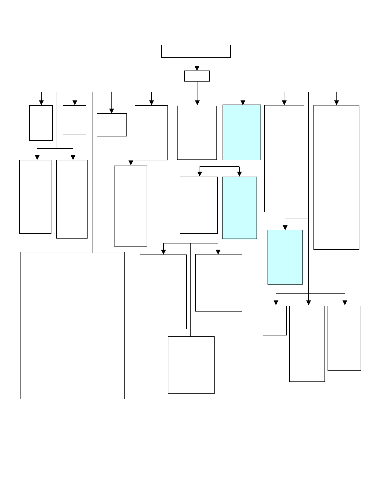
A780 system architecture block diagram shows in Figure 50
PCAP2, RF6003 & RF2722 as a RF modem. And Bulverde controls Blue-tooth, digital
camera etc to be an application processor.
. Neptune-LTE works with
08/02/2003 Motorola Confidential Proprietary 37 / 126
Page 38

A780 Quad-Band Phone Hardware Interface Document Rev. 0.1
4.1 Neptune IC Description
The Neptune IC is a digital baseband processor for the 2 + 2.5G GSM Market. It is a
dual-core processor that contains a Synthesizable Onyx DSP core (566xx), an
ARM7TDMI-S micro controller, and custom peripherals. The Neptune IC is optimized
for 2.5G GSM based applications. The Neptune IC will be ROM-based using mainly
internal memory and an external flash. Also included are mixed signal modules from
MagicLV, Tomahawk, and GCAP3 with a few modifications and additions. The Neptune
IC is optimized for GSM based applications. The Neptune IC is intended to maximize
software re-use from the Patriot family. However, it is expected that software changes
will be necessary to make use of new features.
4.2 Neptune IC Features
Supports only GSM/GPRS.
Integrate 109Kx32 RAM and 792Kx32 ROM accessible by the ARM7TDMI-S
onto Neptune IC. Access to external memories is accessible through external
interface module.
By running most of the application code internally, external bus activity is
minimized reducing radio desense mechanisms.
Digital Modules
a. All memory other than an external flash chip will be included on-chip.
Program storage will be in ROM. This requires a much larger MCU ROM
and MCU RAM.
b. Reference PLL to provide 13MHz clock, the DSP clock and the MCU
clock, that is compensated to the GSM system clock.
c. Real-Time Clock
d. MCU Watchpoint Module that allows for a more efficient patching
method and 64 unique traps.
e. MCU Patch RAM added internally. This patch RAM can be used as DSP
program space in development mode.
f. DMAC DMA and SPI based display port
4.3 Neptune Functional Summary
4.3.1 DSP
The DSP56600 S-ONYXU core in Neptune operates at a maximum output frequency of
104 MHz. This performance will be utilized to support General Packet Radio Service
(GPRS), High Speed Circuit Switched Data (HSCSD), extended Voice Annotation (VA),
Voice Recognition (VR), and other features.
08/02/2003 Motorola Confidential Proprietary 38 / 126
Page 39

A780 Quad-Band Phone Hardware Interface Document Rev. 0.1
1) DSP Memory
The Table 7 below summarizes the DSP memory requirements for the Neptune IC.
Table 7 – Neptune DSP Memory Requirements
2) SP BIST (DBIT)
DBIST is a module to perform self-test on DSP memories. This testing is for both RAM
and ROM’s. RAM built-in self test (BIST) will test the memory arrays, address and data
paths, and control logic around the memory arrays. The fault model is based on IFA-13
which covers all single simple faults: stuck-at, stuck open, transition, coupling, address
decode, data paths, and control logic.
For ROM DBIST makes use of the MISR (Multiple input shift register). The memory is
read and a signature is generated. This signature can be shifted out and compared with
expected signature.
3) DSP Program Paging
The Synthesizable DSP56600 core can only address 64Kx24 of program space at a given
time. Since the Neptune memory requirements exceed this limit, a paging scheme is
necessary to expand the program memory. The paging scheme involves defining a
common block of 32K x 24 shared across all pages from address 0 to address 0x7FFF.
The remaining 32K x 24 of address space are broken into 8K x 24 blocks. Each 8K x 24
08/02/2003 Motorola Confidential Proprietary 39 / 126
Page 40

A780 Quad-Band Phone Hardware Interface Document Rev. 0.1
block can have up to four pages. A page configuration register is required to select which
of the
8K x 24 blocks is in the DSP56600 memory map at a given time. The additional pages
are used for access to the shared Patch RAM (MXRAM).
4) DSP Peripherals
The functions of the DSP peripherals required for the Neptune IC are summarized below.
5) Baseband Port Module (BBP)
The BBP module is a full-duplex (56602 SSI) serial port that interfaces to the on-chip TX
and RxCPROC modules. Capability has been built into the module to allow for multiple
time slots receive and transmit sequences. The Base Band Port (BBP) provides a fullduplex serial port for serial communication with integrated analog baseband modules.
The BBP consists of independent transmitter and receiver sections, receiver and
transmitter counters and a common BBP clock generator
6) Layer1 Encryption Module (LEM)
The Layer1 Encryption module is GSM-specific module that performs the generation of
the A5 receive and transmit ciphering sequences. Additionally, it provides acceleration
for GSM FIRE code decoding and encoding.
7) DSP Timer Module (DTIMER)
The DSP DTIMER module is a general-purpose timer with three separate timing
channels with the associated triggers and interrupt enables.
8) Serial Audio CODEC Port (SAP)
The SAP module, like the BBP, is based on a standard SSI (DSP56602 SSI) port, and is
included for DAI testing, or, for development, communication with external serial audio
CODEC. A programmable BRM is provided to divide down the reference clock to the
desired frequency when the module itself is required to source the serial clock.
9) Direct Memory Access Controller (DMA)
One DMA channel is provided to support bi-directional transfers for the BBP and SAP
modules. Several packing and unpacking modes are supported.
10) Viterbi Accelerator (VIAC)
The VIAC is a Viterbi decoder accelerator that supports the GSM full and half rate
channel coding schemes, that is, constraint length codes 5 and 7, and 1/2, 1/3, and special
08/02/2003 Motorola Confidential Proprietary 40 / 126
Page 41

A780 Quad-Band Phone Hardware Interface Document Rev. 0.1
1/6 rate codes. Additionally, it provides acceleration for adaptive channel equalization,
also utilizing Viterbi methods.
11) DSP Special Interrupt Handler (DSIH)
Since the DSP56600 core is limited to eight peripheral interrupt signals, and Neptune has
more than eight DSP peripheral interrupt sources, some of the interrupt signals must be
OR’ed together. This function is handled by the DSP Special Interrupt Handler module.
In cases when more than one of the OR’ed interrupts occurs at the same time, a fixed,
hardware priority scheme is used by DSIH.
12) SP On Chip Emulator Debug Module (OnCE)
The DSP on-chip emulation (OnCE) module provides a means of interacting with the
DSP core and its peripherals non-intrusively so that a user may set breakpoints, examine
registers, memory, or on-chip peripherals facilitating hardware/software development.
The OnCE controller functionality is accessed through the JTAG port.
13) DSP Debug Module (PDDM)
The DSP Debug supplies watchpoint and externally visible trace as defined below.
X/Y Data Watchpoints:
• The data watchpoints provide one set of comparators for each of the X and Y address
and data buses. The data watchpoints provide the capability to match any combination of
partial data and data address range and R/W. Data watchpoint events are observable
through a s/w selectable GPIO pin, a DSP interrupt, or a DSP debug event.
Program Address Watchpoints:
• The program address watchpoints provide one comparator for the DSP Program address
and page select bits. The ability to match a program address range is not required.
Program Address watchpoint events are observable through a s/w selectable GPIO pin, a
DSP interrupt, or a DSP debug event.
Program Address Trace (PAT):
• The DSP program address bus, page select bits, and a valid strobe are available on the
development package part through a set of GPIO pins.
14) Voice CODEC (VOCOD)
Voice CODEC consists of voice coding and voice decoding. The voice coding function
takes human speech signal in voltage format then converts it to 8 KHz digital signals. The
voice decoding function takes 8 kilo-samples per second digital signal then converts it to
an audible voice signal in voltage format.
08/02/2003 Motorola Confidential Proprietary 41 / 126
Page 42

A780 Quad-Band Phone Hardware Interface Document Rev. 0.1
15) DSP Clock Generator (DCLKG)
The DSP Clock Generator module provides clocks for the DSP Core, the DSP Memories,
and the DSP Peripherals. The control of this module is supported by the registers in the
CCM module.
16) IC Identification Module (IIM)
The IIM consists of two functions: the Unique Identifier (UID) and the Hardware
Revision Register (REV).
The Unique Identifier cell is a laser programmed register that is programmed to a unique
value for each die produced. The Unique Identifier is a 128 bit wide value that is
accessible from the PIG bus interface to the MCU.
The Hardware revision register is simply a 16-bit read-only register that is fixed in value.
The value is changed in layout whenever a silicon change is performed. This provides the
software with a knowledge of what hardware features are available in the current
revision. The value in the REV register must be programmable in metal only to allow for
metal mask changes to be detected in software. The register is readable only by the MCU.
17) Clock Monitor (CMON)
The Clock monitor module contains a custom cell that detects when the system clock has
not transitioned for a given period of time. The Clock Monitor will signal the Watchdog
module to generate a Watchdog event when a clock edge is not detected for 150ns to
620ns at its input. The clock monitor operates on the output of the crystal oscillator
module, not the REFPLL. The clock monitor will be disabled automatically in hardware
when entering deep sleep (crystal oscillator shut off). The clock monitor will provide
software the ability to disable it.
18) Power On Reset (POR)
The POR circuit will provide a reset upon Power Up to be used in certain circuits in the
chip that need to be working during RESET. The output of this circuit will also be OR’ed
in the chip Reset circuit to activate the chip reset during power up.
This circuit will have three main elements:
• POR - Power On Reset System that recognizes the power up.
• A ring oscillator to generate clocks during the POR period.
• A Counter to count ring oscillator cycles.
19) System JTAG Controller (SJC)
The Neptune IC has an integrated S-ONYXU DSP and ARM7TDMI-S MCU on the
same die and includes two JTAG TAP controllers. The ARM MCU ICEBreaker TAP
08/02/2003 Motorola Confidential Proprietary 42 / 126
Page 43

A780 Quad-Band Phone Hardware Interface Document Rev. 0.1
controller, the ONYXU DSP OnCE™ TAP controller, and the Neptune System JTAG
TAP controller.
The external JTAG pins are connected to the Neptune System JTAG TAP controller and
through JTAG instructions the user may select one of three emulation modules for
programming. The user may activate each of the three emulation modules separately or
any combination of them simultaneously.
The System JTAG Controller (SJC) will support modes that allow stand-alone ARM and
ONYXU tools to work separately or simultaneously, if desired.
4.3.2 ARM7 MCU
The ARM7TDMI-S is a member of the ARM family of general-purpose 32-bit
microprocessors. The ARM family offers high performance for very low power
consumption and gate count.
The ARM7 MCU core in Neptune operates at a frequency up to 52 MHz. The increase in
processor frequency will increase performance of critical routines located in internal
memory. Examples of these routines include: Virtual DMA, V.42bis compression, GPRS
support, and the RTOS executive.
4.3.2.1 MCU Memory
Neptune has 901Kx32 of internal memory accessible by the MCU. A 792Kx32 block of
internal memory will be implemented as ROM, while the remaining 109Kx32 block will
be implemented as RAM.
4.3.2.2 MCU Peripherals
The functions of the MCU peripherals for the Neptune IC are summarized below. Each
peripheral provides the ability to disable the clock at the input to the module. Each
peripheral provides a software reset capability. The software reset must reset the
peripheral in the same way as a system reset. Neptune includes some clock control logic
outside of the peripheral blocks. The Clock Control Module handles this supplemental
clock control.
1) ARM7 Platform Core Arbiter (CARB)
The ARM7 core does not support alternate bus masters. The CARB module is added to
support alternate masters. In Neptune, it interfaces exclusively to the AMARB, the
Alternate Master Arbiter. All modules that require bus access interface to the AMARB.
2) ARM External Interface Module (AEIM)
The External Interface Module (EIM) handles the interface to external devices, including
generation of chip selects for external peripherals and memory. It contains the following
features:
08/02/2003 Motorola Confidential Proprietary 43 / 126
Page 44

A780 Quad-Band Phone Hardware Interface Document Rev. 0.1
• Six Chip Selects for external devices, each covering a range of 16Mbytes
• Programmable Wait-State generator for each Chip Select
• Selectable Protection for each Chip Select
• Programmable Data Port Size for each Chip Select
• Control for external/internal Boot ROM device selection
• MCU Bus Monitor counter for all bus cycles
• Programmable general output capability for unused Chip Select outputs
• Show cycles to allow internal bus cycles to be externally monitored
• 20 dedicated General Purpose Outputs
• Synchronous Burst-mode support for most industry standards flash device
3) ARM Peripheral Interface Gasket (APIG)
The APIG module interfaces the R-AHB to the external 3-cycle PIG bus. The Neptune
contains two of these modules.
4) ARM IPBus Interface (AIPI)
The AIPI module interfaces the R-AHB to the internal IPBus.
5) Alternate Master Arbiter (AMARB)
The alternate master arbiter allows multiple alternate masters, such as the DMAC, GEM,
or TCM, to gain control of the ARM7TDMI-S platform bus. The alternate master arbiter
is also used during low power modes to gate the clock to the ARM7TDMI-S core.
6) Multiple Queue Serial Peripheral Interface (MQSPI)
The MQSPI provides two (2) independent QSPI channels which performs the serial
programming operations to configure the RF subsystem and selected peripherals. It is
designed to minimize the amount of MCU interaction by automating multiple and
repetitive serial data transfers. The module has multiple queues to hold these transfers.
Module transfers can be triggered by the Layer 1 Timer.
7) ARM7TDMI-S Interrupt Controller (AITC)
The ARM7TDMI-S Interrupt Controller collects interrupt requests from up to 64 multiple
sources and provides an interface to the ARM7TDMI-S core for normal and fast
interrupts. The AITC includes hardware acceleration of normal interrupt to quickly jump
to the highest priority interrupt service routine, effectively providing a vectored interrupt
mechanism.
8) SIM Interface Modifications (SIM)
08/02/2003 Motorola Confidential Proprietary 44 / 126
Page 45

A780 Quad-Band Phone Hardware Interface Document Rev. 0.1
The SIM module is a customized UART with additional features allowing for
communication with SmartCards and conforming to the ISO 7816 specification. The
module has a transmit buffer of 16 bytes. The receive buffer is 32 bytes.
9) Universal Asynchronous Receiver Transmitter (UART)
A UART module performs all normal operations associated with “start-stop”
asynchronous communications. The UART transmit and receive buffer sizes are 32 bytes
each. The UART modules will operate at 115.2Kbps, 460Kbps, and 920Kbps based on a
13MHz input reference clock.
10) Deep Sleep Module (DSM)
The Deep Sleep Module allows for optimal power savings in idle modes by allowing the
Neptune IC to synchronize to the frame timing automatically even though the timing
reference has been removed from the part during the idle time.
11) Watchdog Timer (WDOG)
The Watchdog Timer is used to protect against system failures by providing a means to
escape from unexpected events or application errors. Once started, the timer must be
serviced by the core on a periodic basis. If servicing does not occur, the module times out
and asserts the reset signal.
12) General Packet Radio Service Encryption Module (GEM)
The GPRS Encryption Module (GEM) is a hardware accelerator designed to assist in the
encryption/decryption of General Packet Radio Service (GPRS) data packets and
generation/verification of
Frame Check Sequence (FCS) information contained in GPRS data packets. The GEM is
required to arbitrate with the MCU for direct access to memory (DMA). This allows the
GEM access to any internal or external memory space, but interrupts all MCU activity
until the GEM relinquishes the bus.
13) Keypad Port (KPP)
The Keypad port is a module that is used for keypad matrix scanning.
14) Enhanced General Purpose Timer (EGPT)
The EGPT provides 3 output compare, 2 input capture, and one PWM channel. An
Enhanced Periodic Interrupt Timer (EPIT) is included in the EGPT. The EPIT contains a
24-bit down-counter with programmable modulus that can generate an interrupt when the
counter reaches zero.
08/02/2003 Motorola Confidential Proprietary 45 / 126
Page 46

A780 Quad-Band Phone Hardware Interface Document Rev. 0.1
15) Test Control Module (TCM)
The TCM module contains the logic that controls the various test features for the Neptune
IC. Any feature that is not useful for debug in functional mode will be conditioned with
the Neptune TEST [2:0] input pins.
The following functions are provided by the TCM module:
• Test Mode Definitions
• MCU/DSP Peripheral Scan Test
• MCU/DSP Scan Test
• AMT Mode
• Analog Signal observability
• Non Scan Test
• Analog module output selection and configuration
• Memory bit mapping and functional testing at speed
• Memory BIST for DSP and ARM7 Memories
• IDDQ
• Scan Divergence
• DSP Scan Test
16) MCU Watchpoint (AWPT)
The Watch Point Module is a 32-bit peripheral which can be used to either patch source
code routines or fix data tables in the Read-Only Memory (ROM). The AWPT supports
up to 64 addresses which can be patched where 4 are any location within memory and 60
are dedicated to ROM patching. Alternatively, 16 of the 64 locations can be used as a 1word data fix. Alternatively, the 4 generic locations can be used to generate a break point
event to the ARM7TDMI-S.
17) USB Digital Phase Locked Loop (REFPLL)
The USB Digital Phase Locked Loop (REFDPLL) is used to generate the 48Mhz
frequency required for the USB module. Lock times on the DPLL module will be less
than 50us. The DPLL must not require the use of an external capacitor.
18) Real Time Reference (RTR)
The RTR module is a simple 47-bit up counter that runs at the always present 32.768Khz
input frequency.
The counter is read-only, and is intended to provide software with a time reference to the
last system reset event. The module is capable of generating a periodic interrupt
whenever one of the lower 16 bits of the counter is set. This is intended to provide the
ability to profile the operation of the system software.
08/02/2003 Motorola Confidential Proprietary 46 / 126
Page 47

A780 Quad-Band Phone Hardware Interface Document Rev. 0.1
19) Real Time Clock (RTC)
The real time clock (RTC) module consists of counters and registers used to maintain the
day, time of day and alarm values. The RTC operates even when the phone is powered
down and the alarm function can turn it on and alert the processor. If the phone is already
on, the processor is interrupted. The RTC uses a frequency reference generated on the
PCAP2 using a low-cost crystal and inaccuracies in the frequency may be compensated
for by trimming the modulus register value. The RTC module also provides power cut
logic, and keep-alive memory that activates when a low battery condition is detected.
20) Display Memory Access Controller (DMAC)
The DMAC (display memory access controller) module is designed to transfer data from
the display frame buffer in system memory to an external LCD display device. The
DMAC can support 4-bit serial, 3-bit serial, and 8 bit parallel transfers. The DMAC acts
as a master on the system bus and transfers the data transparently, with minimal software
intervention. Bus utilization of the DMAC is deterministic and controllable via the
programmability of the DMAC and alternate master arbiter.
21) Clock Control Module (CCM)
The Clock Control Module handles all intermodule clock routing, the selection of
multiple input clock sources for the cores and various peripherals, manage MCU low
power modes (DOZE, STOP and WAIT) by disabling peripheral clocks and other clock
related features. This module also includes the control logic for asserting soft and hard
chip-level system resets.
22) External Interrupt Module (INT)
This module provides control for five of the eight external interrupt sources. Each pin is
individually configurable as a level-sensitive interrupt, an edge-detecting (rising, falling,
or both) interrupt, or a general purpose I/O. Each pin has a dedicated interrupt line.
23) Analog to Digital Interface (A2DIGL)
This module provides control for eight external interrupt sources. Each pin is individually
configurable as a level-sensitive interrupt, an edge-detecting (rising, falling, or both)
interrupt, or a general purpose I/O.
The A2DIGL is a digital module intended for control of mixed signal modules. The
A2DIGL is divided into two parts: One part contains SPI Interface control; while the
other part contains the MCU-based GPADC digital control. The mixed-signal new
modules are: REGUL, GPADC, TOSW, and TUNEC. The mixed-signal re-used modules
(from MAGIC-LV, GCAP, and Tomahawk) are: PAC, TX, TRSYNT, DCADAPT,
RxSDG, RxAFE, and RXCPROC. The re-used logic ensures a high degree of backward
compatibility with the Patriot program software.
08/02/2003 Motorola Confidential Proprietary 47 / 126
Page 48

A780 Quad-Band Phone Hardware Interface Document Rev. 0.1
4.3.3 Shared Peripherals
Shared peripherals are peripherals that can be accessed by both the DSP and MCU cores.
The functionality of these peripherals is detailed below.
4.3.3.1 Patch RAM (MXRAM)
The Patch RAM will be used by the DSP for development and then reconfigured to MCU
Patch RAM for production. Therefore, MCU code will be developed in external flash and
then internal ROM for production and DSP code will be developed in internal RAM (no
external DSP bus) and ROM for production. The memory will be organized 32bits wide,
therefore for DSP development one byte of each location will be unused. The core to
which the MXRAM is connected is controlled by a selector bit in the TCM.
4.3.3.2 Universal Serial Bus Module (USB)
The USB module provides the required buffering and protocol to communicate on the
Universal Serial Bus. The module is provided with an access port for the DSP and for the
MCU. The module will act as a USB device only. Host functionality will not be
supported. All four types of USB data transfers are supported: control, isochronous,
interrupt, and bulk. Endpoint 0 always functions as a bidirectional control endpoint with
an eight (8) byte buffer.
4.3.3.3 General Purpose I/O (GPIO)
The GPIO module is a stand alone module that serves as the all-in-one communication
link between the outside world, the MCU module, and the DSP module. The GPIO
module will be implemented as a stand-alone module. The GPIO module will provide the
following functionality:
• Standard GPIO functionality
• Multiplexed output functionality
• Alternate input functionality
• Shared Access for DSP and MCU
• MCU, DSP interrupt capability
• Interrupt visibility
4.3.3.4 MCU / DSP Interface (MDI)
The MDI is the communication interface between the DSP and MCU cores. Through this
module, each core can access shared memory, messaging registers, and flags. This
module also allows each core to interrupt the other, monitor the low power state of the
other core, and other useful functions.
4.3.3.5 Layer 1 Timer (L1T)
08/02/2003 Motorola Confidential Proprietary 48 / 126
Page 49

A780 Quad-Band Phone Hardware Interface Document Rev. 0.1
The Layer 1 Timer module allows for control of all the radio channel timings. Its main
function is to unload the MCU from having to schedule events associated with the radio
air interface. The timer provides the user a great deal of flexibility in scheduling and
executing events using the programmable event tables and macros.
4.4 Neptune GPIO Summary
Neptune GPIO module is a stand alone module that serves as the all-in-one
communication link between the outside world, the MCU module and the DSP module.
The GPIO communicates with the MCU through the IP Bus and to the DSP through the
DSP Peripheral Bus. The GPIO module houses five 16 pin bi-directional Ports.
Neptune GPIO has the following features:
Five 16 pin bi-directional Ports (A- E)
Alternate output function to select 1 of up to 8 output paths for each GPIO pin
Alternate input function to select 1 of up to four input paths for each GPIO pin
Shared Port Data Access for DSP and MCU
MCU, DSP interrupt capability with selectable rise/fall edge triggered or high/low
level sensitive interrupts for MCU interrupt
Interrupt status register with “write-one-to-clear” for MCU interrupt
Internal interrupt visibility of any of 64 interrupts
Bus Master Mode functionality
MuxDFF SCAN mode functionality
DSP Address Trace Mode and DSP Master Mode I/O
Scan Divergence Mode functionality
Bist Mode functionality
The usage of Neptune GPIO in A780 is listed in Table 8
and Table 9.
08/02/2003 Motorola Confidential Proprietary 49 / 126
Page 50

A780 Quad-Band Phone Hardware Interface Document Rev. 0.1
GPIO Module Name A780 Label Description
PA0 TRACE CKO NC /
PA1 A2DIGL RX_EN_OUT NC /
PA2 L1T TOUT5 OW_DATA Battery EPROM data line
PA3 A2DIGL GSM*_DCS NC /
PA4 L1T TOUT7 TXST Transmit enable
PA5 L1T TOUT8 ENR RFMD control.
PA6 L1T TOUT9 EXT_BP_EN EMU Bus Support
PA7 L1T TOUT10 TX_EN_B RFMD control.
PA8 L1T TOUT11 RX_EN RFMD control.
PA9 INT INT0 nPWR_EN Bulverde sleep indicator signal.
PA10 INT INT1 PCAP_PRI_INT PCAP SPI interrupt
PA11 USB USB_SUSPEND NC /
PA12 INT INT3 TP_MM_EN Bulverde multimedia application indicator.
PA13 INT INT4 NC /
PA14 WDOG WDOG* BB_WDI Neptune Watchd og signal.
PA15 SAP SC0A CLKR A780 used as RFMD control.
PB0 SAP SC1A FSR A780 used as RFMD control.
PB1 SAP SCKA SAP_CLK SAP clock signal.
PB2 SAP STDA SAP_TXD SAP transmitting signal.
PB3 SAP SC2A SAP_FRM SAP frame signal.
PB4 SAP SRDA SAP_RXD SAP receiver signal.
PB5 UART2 TXD2 NEP_UTXD2 A780 used as AGPS control.
PB6 UART2 RXD2 NEP_URXD2 A780 used as AGPS control.
PB7 SIM SIM_RST SIM_RST SIM card reset control.
PB8 SIM SIM_PD BATT_DETB SIM card presence detection.
PB9 SIM SIM_CLK SIM_CLK SIM card clock signal.
PB10 SIM SIM_DIO SIM_DIO SIM card data I/O signal.
PB11 SIM SIM_VCCEN VSIM_EN SIM card power supply enable signal.
PB12 DMAC SDATA (LCD_DATA[7]) NC /
PB13 DMAC LCD_CLK (LCD_DATA[6]) NC /
PB14 DMAC LCD_CS NC /
PB15 DMAC LCD_RS NC /
PC0 UART1 CTS1 NC /
PC1 JTAG RTCK NC /
PC2 GPADC ADC_SYNC CLK_13MHz PCAP 13MHz clock Input
PC3 KPP COLUMN0 FLIP_SW A780 used as Flip status indicator.
PC4 KPP COLUMN1 NC /
PC5 KPP ROW0 BB_WDI2 Hand-shake signal between Neptune & Bulverde.
PC6 KPP ROW1 NC /
PC7 KPP ROW4 BP_RDY Hand-shake signal between Neptune & Bulverde.
Table 8 – Neptune GPIO Usage Assignment (PA0 ~ PC7)
08/02/2003 Motorola Confidential Proprietary 50 / 126
Page 51

A780 Quad-Band Phone Hardware Interface Document Rev. 0.1
GPIO Module Name A780 Label Description
PC8 KPP ROW5 BP_ROW5 Neptune used this signal to shutdown PCAP (WDI)
PC9 INT INT6 NC /
PC10 KPP ROW6 MCU_INT_SW Hand-shake signal between Neptune & Bulverde.
PC11 KPP ROW7 NC /
PC12 GPIO PC12 NC /
PC13 JTAG SJC_MOD NC /
PC14 GPIO PC14 NC /
PC15 MQSPI SPI_CS6 NC /
PD0 A2DIGL RF_CLK RF_CLK RF MQSPI clock signal.
PD1 A2DIGL RF_DATA RF_DATA RF MQSPI MOSI signal.
PD2 A2DIGL RF_CS RF_CS RF MQSPI frame signal.
PD3 MQSPI QSCKA BB_SPI_CLK SPI clock signal to PCAP2.
PD4 MQSPI MISOA BB_SPI_MISO SPI MISO signal to PCAP2.
PD5 MQSPI MOSIA BB_SPI_MOSI SPI MOSI signal to PCAP2.
PD6 MQSPI SPI_CS0 NC /
PD7 MQSPI SPI_CS1 NC /
PD8 MQSPI SPI_CS2 NC /
PD9 MQSPI SPI_CS3 PCAP_CS SPI chip select signal to PCAP2.
PD10 USB USB_TXENB ICL_TXENB A780 USB ICL signal.
PD11 USB USB_VPIN ICL_VPIN A780 USB ICL signal.
PD12 USB USB_VMIN ICL_VMIN A780 USB ICL signal.
PD13 USB USB_XRXD ICL_XRXD A780 USB ICL signal.
PD14 USB USB_VPOUT ICL_VPOUT A780 USB ICL signal.
PD15 USB USB_VMOUT ICL_VMOUT A780 USB ICL signal.
PE0 UART1 URTS1 NC /
PE1 L1T TOUT12 nGAM_RESET AGPS reset signal in A780.
PE2 MQSPI SPI_CS8 DRI A780 used this as RFMD control.
PE3 AEIM EBW* NC /
PE4 DMAC LCD_DATA[0] NC /
PE5 DMAC LCD_DATA[1] NC /
PE6 DMAC LCD_DATA[2] NC /
PE7 DMAC LCD_DATA[3] NC /
PE8 DMAC LCD_DATA[4] NC /
PE9 DMAC LCD_DATA[5] NC /
PE10 GPIO PE10 NC /
PE11 GPIO PE11 NC /
PE12 GPIO PE12 NC /
PE13 UART2 CTS2 NEP_UCTS2 A780 used as AGPS control.
PE14 MQSPI MISOB NC /
PE15 UART2 RTS2 NEP_URTS2 A780 used as AGPS control.
Table 9 – Neptune GPIO Usage Assignment (PC8 ~ PE15)
08/02/2003 Motorola Confidential Proprietary 51 / 126
Page 52

A780 Quad-Band Phone Hardware Interface Document Rev. 0.1
T
[
[
]
]
4.5 Neptune-LTE Memory Interface
Although Neptune has internal ROM and RAM, it still needs external memory chipsets
for its operation. One 32Mbit Flash and one 4Mbit SRAM can access by Neptune via the
16-bit parallel data bus. Each of these devices is assigned a specific chip enable(s) from
the Neptune-LTE. Within the Neptune chip select control register; the wait states are
defined for each device. Each wait state is the equivalent of one clock cycle, i.e. 1 /
13MHz = 77 ns. The memory chip selected for A780 Neptune-LTE baseband system is a
stack-memory by which both Flash and (P)SRAM are embedded into one single 8.0mm
by 10mm Stacked-MSP (Chip Scale Package) for PCB space saving. Figure 13
shows
this stack-memory block diagram in which both Flash and SRAM devices are included.
ADV#
A
VCC
OE#1
CE#1
CLK
WP#
RST#
20:19
28F640W18
FLASH
(64Mbits)
VCCQ
WE#
VPP
WAI
VSS
A [18:0
D
15:0]
S-VCC
S-CS1
S-CS2
R-OE#
SRAM
(16Mbits)
R-WE#
R-UB#
R-LB#
Figure 13 – A780 Baseband 64W18 + 8MB SRAM Stacked-CSP Block Diagram
The detailed information of Flash and SRAM is described as following.
4.5.1 Flash
The Flash used in A780 phone design is Intel W18 series Flash product. The 1.8 Volt
Intel® Wireless Flash memory provides RWW/RWE capability with high performance
synchronous and asynchronous reads on package-compatible densities with a 16-bit data
bus. Individually erasable memory blocks are optimally sized for code and data storage.
Eight 4-Kword parameter blocks are located in the parameter partition at either the top or
08/02/2003 Motorola Confidential Proprietary 52 / 126
Page 53

A780 Quad-Band Phone Hardware Interface Document Rev. 0.1
bottom of the memory map. The rest of the memory array is grouped into 32-Kword main
blocks.
The memory architecture for the 1.8 V Intel Wireless Flash memory consists of multiple
4-Mbit partitions, the exact number depending on device density. By dividing the
memory array into partitions, program or erase operations can take place simultaneously
during read operations. Burst reads can traverse partition boundaries, but user application
code is responsible for ensuring that they don’t extend into a partition that is actively
programming or erasing. Although each partition has burst-read, write, and erase
capabilities, simultaneous operation is limited to write or erase in one partition while
other partitions are in a read mode.
Augmented erase suspend functionality further enhances the RWW capabilities of this
device. An erase can be suspended to perform a program or read operation within any
block, except that which is erase-suspended. A program operation nested within a
suspended erase can subsequently be suspended to read yet another memory location.
After device power-up or reset, the 1.8 Volt Intel Wireless Flash memory defaults to
asynchronous read configuration. Writing to the device’s configuration register enables
synchronous burst-mode read operation. In synchronous mode, the CLK input increments
an internal burst address generator. CLK also synchronizes the flash memory with the
host CPU and outputs data on every, or on every other, CLK cycle after initial latency. A
programmable WAIT output signal provides easy CPU-to-flash memory synchronization.
In addition to its enhanced architecture and interface, the 1.8 Volt Intel Wireless Flash
memory incorporates technology that enables fast factory programming and low-power
designs. The EFP option renders the fastest available program performance, which can
increase a factory’s manufacturing throughput.
The device supports read operations at 1.8 V VCC and erase and program operations at
1.8 V or 12V VPP. With the 1.8 V VPP option, VCC and VPP can be tied together for a
simple, ultra-low power design. In addition to voltage flexibility, the dedicated VPP input
provides complete data protection when VPP ≤ VPPLK.
A 128-bit protection register enhances the user’s ability to implement new security
techniques and data protection schemes. Unique flash device identification and fraud-,
cloning-, or content- protection schemes are possible via a combination of Intelprogrammed and user-OTP data cells.
Zero-latency locking/unlocking on any memory block provides instant and complete
protection for critical system code and data. An additional block lock-down capability
provides hardware protection where software commands alone cannot change the block’s
protection status.
The device’s CUI is the system processor’s link to internal flash memory operation. A
valid command sequence written to the CUI initiates device WSM operation that
automatically executes the algorithms, timings, and verifications necessary to manage
flash memory program and erase.
An internal status register provides ready/busy indication results of the operation
(success, fail, etc.).
08/02/2003 Motorola Confidential Proprietary 53 / 126
Page 54

A780 Quad-Band Phone Hardware Interface Document Rev. 0.1
Three power-savings features, APS, standby, and RST#, can significantly reduce power
consumption. The device automatically enters APS mode following read cycle
completion.
Standby mode begins when the system deselects the flash memory by de-asserting CE#.
Driving RST# low produces power savings similar to standby mode. It also resets the part
to read array mode (important for system-level reset), clears internal status registers, and
provides an additional level of flash write protection.
4.5.2 SRAM
The memory size used in A780 phone design is 16 Mega bits (2 Mega bytes).
4.5.3 Neptune-LTE Chip Select Assignments
The ARM External Interface Module (AEIM) handles the interface to devices external to
an ARM architecture based chip, including generation of chip selects for external
peripherals and memory.
It contains the following features:
Six Chip Selects for external devices, each covering an unrestricted address range
Programmable Wait-State generator for each Chip Select
Selectable Protection for each Chip Select
Programmable Data Port Size for each Chip Select
Bus Watchdog counter for all bus cycles
Programmable general output capability for unused Chip Select outputs
Show cycles to allow internal bus cycles to be externally monitored
Synchronous Burst Mode support for industry standard flash devices
20 dedicated General Purpose Outputs
Address suppression during burst mode operations
The six Chip Selects assigned as in Table 10
.
Pin Name Pin # Type Active H/L Description
CS0 P15 O L Flash Chip Selection
CS1 R15 O L SRAM Chip Selection
Table 10 – Neptune-LTE Chip Select Assignment
EB0 * and EB1 * are assignment as the Byte selection for SRAM access. EB0 * is for
SRAM lower byte and EB1 * is for SRAM upper byte access.
08/02/2003 Motorola Confidential Proprietary 54 / 126
Page 55

A780 Quad-Band Phone Hardware Interface Document Rev. 0.1
K
T
_
[
]
[
]
[
[
[
The memory connection with Neptune-LTE shows in Figure 14
.
Neptune-LTE
BURSTCL
ECB
CS0
LBA
R_W
D
15:0
OE
Data Bus (D [15:0])
CLK
WAI
CE
ADV
WE
OE
D [15:0]
FLASH
(64Mb)
A
Add. Bus (A [23:0])
23:1
A
21:0]
D
EB1
EB0
CS1 R_CS
15:0]
A
19:0]
R_OE
R_WE
R_UB
R
LB
SRAM
(16Mb)
Figure 14 – A780 Baseband Neptune-LTE and Memory Connection Block Diagram
08/02/2003 Motorola Confidential Proprietary 55 / 126
Page 56

A780 Quad-Band Phone Hardware Interface Document Rev. 0.1
4.6 Neptune MQSPI Module
The MQSPI (Multiple Queue Serial Peripheral Interface) performs the serial
programming operations to configure radio subsystems and selected peripherals. In this
dual SPI configuration, the system is typically partitioned into RF and baseband
functions. This peripheral is designed to minimize the amount of MCU interaction
necessary for multiple serial data transfers. The MQSPI module in Neptune has the
following features:
Full-Duplex, Three-Wire Synchronous Transfers
Half-Duplex, Two-Wire Synchronous Transfers
Programmable Bit Rates
Programmable Inactive Clock Polarity
Programmable Chip Select Polarity
Ten Chip Select Pins
256 X 16 bit of RAM for Data I/O Storages sharable by both SPIs
Programmable Transfer Length - from 1 to 32 Bytes
Programmable Multiple Message - from 1 to 64 Messages
Each SPI functions only as a master SPI
Dual Independently Functioning SPIs
32 Configurable Control Queues/Triggers
64 Programmable Control Data Registers (32 Mode and 32 Pointer Registers)
Four FIFO Queues - a High and Low Priority Queue for Each SPI
32 One-Cold Trigger Signals From the Layer 1 Timer
MCU Controlled Trigger Register
Two Interrupt Lines - One for Each SPI
Programmable Data Change on Rising/Falling Clock Edge
Programmable Data Latch on Rising/Falling Clock Edge
Separate Read/Write Data I/O Storage Pointers
Burst and multiple message transfers
Programmable 128 Clock Delay Before First Clock Edge
Programmable 128 Clock Delay After Transfer
Transmit and receive Data is LSB/MSB Selectable
DOZE Mode Capability
Serial Display Interface
A780 quad-band EDGE / GPRS GSM uses a dedicated RF SPI port for RF6003 and
RF2772 data writing. And one MQSPI port is used to access with PCAP2 and the chip
selection is SPI_CS3. The connection between Neptune-LTE and PCAP2, RF6003,
RF2722 shows in Figure 15
.
08/02/2003 Motorola Confidential Proprietary 56 / 126
Page 57

A780 Quad-Band Phone Hardware Interface Document Rev. 0.1
A
K
SDI
SCLK
SSB
SDI
SCLK
SSB
RF_DATA
RF_CLK
RF_CS
RF_DATA
RF_CLK
RF_CS
Neptune-LTE
SPI_CS3
QSCKA
MOSIA
MISO
PCAP_CS
BB_SPI_MOSI
BB_SPI_CL
BB_SPI_MISO
RF2722
RF6003
PRICE
PRISPICLK
PRIMOSI
PRIMISO
PCAP2
Figure 15 – Neptune MQSPI Connection with PCAP2 and RF6003 Block Diagram
The MQSPI of Neptune-LTE to RF6003 and RF2722 shares one chip-select signal, that
due to the fact that RF6003 and RF2722 registers mapped to different memory locations.
RF6003 SPI controlled registers address and descriptions illustrated in Table 12
.
RF2722 SPI controlled registers address and descriptions illustrated in Table 11
.
Register Address Description
CRX1 100000 AGC, Standby modes and test output select
CRX2 100001 DCOC and GPO
CRX3 100010 DCOC
CRX4 100011 DCOC
CRX5 100100 TX buffer, LNA, VCO, Mixer current settings
CF2 100101 Gain settings for the polyphase filters and LNA's
Reserved 100110 Reserved for future use
Reserved 100111 Reserved for future use
Reset 011111 Writing this address resets all SDI bits to their default states
Table 11 – RF2722 Register Map
08/02/2003 Motorola Confidential Proprietary 57 / 126
Page 58

A780 Quad-Band Phone Hardware Interface Document Rev. 0.1
Register Address Description
CFG1 000000 Configuration 1
CFG2 000001 Configuration 2
CFG3 000010 Configuration 3
OFFS 000011 Frequency Offset
AFCD 000100 Digital AFC Offset
PLLx0 000101 PLL 0
PLLx1 000110 PLL 1
PLLx2 000111 PLL 2
TXMOD 001000 TX Modulator Register
PARMP1 001001 PA Ramp 1
PARMP2 001010 PA Ramp 2
PARMP3 001011 PA Ramp 3
PARMP4 001100 PA Ramp 4
PARMP5 001101 PA Ramp 5
PARMP6 001110 PA Ramp 6
PARMP7 001111 PA Ramp 7
PARMP8 010000 PA Ramp 8
PARMP9 010001 PA Ramp 9
PARMP10 010010 PA Ramp 10
PARMP11 010011 PA Ramp 11
DAC1 010100 DAC 1 Control
DAC2 010101 DAC 2 Control
CAL 010110 Calibration
TRSW 010111 Transmit Switch Control
PGAIN 011000 PMod Phase Path Gain
AMPM1 011001 AM to PM Correction 1
AMPM2 011010 AM to PM Correction 2
AMAM1 011011 AM to AM Correction 1
AMAM2 011100 AM to AM Correction 2
AGAIN 011101 Amplitude Path Gain
TEST 011110 Test
CAL2 110000 Calibration 2
SSI 110001 SSI Configuration
AEDGE 110010 Analog EDGE
BLANK 110011 BLANK
DELAY 110100 DELAY
Table 12 – RF6003 Register Map
08/02/2003 Motorola Confidential Proprietary 58 / 126
Page 59

A780 Quad-Band Phone Hardware Interface Document Rev. 0.1
K
K
K
N
4.7 SIM Interface
The SIM Interface Module (SIM) is designed to facilitate communication to SIM cards or
Eurochip pre-paid phone cards. The SIM module has two ports that can be used to
interface with the various cards. The SIM connection in A780 shows in Figure 16
diagram.
Neptune-LTE
SPI_CS3
QSCKA
MOSIA
MISOA
SIM_RST
SIM_CLK
SIM_VCCEN
SIM_DIO
SIM_PD
SIM_VCC
SIM_RST
SIM_CL
SIM_DIO
C1
C2
C3
R802
5.6
C5
C6
C7
PCAP2_CS
BB_SPI_MOSI
BB_SPI_CL
BB_SPI_MISO
VSIM_EN
BATT_DETB
SIM_VCC
PRICE
PRISPICLK
PRIMOSI
PRIMISO
PCAP2
VSIM_E
(SPI Bit)
VSIM
B+
Figure 16 – A780 SIM Connection Block Diagram
A780 doesn’t use PCAP2 internal level shifters for 5V SIM card support due to the fact
that Neptune-LTE multiplexed the SIM data input and output together. A780 can only
support 3V SIM card and no 1.8V & 5V SIM support.
The SIM detect circuit is actually a battery detection circuit in A780 design. When one of
the following conditions occurs, the BATT_DETB output asserted logic 0 to indicate
battery presence.
A thermistor (with effective resistance < 38K approx) is connected to the AD4
input
The BATT+ (battery) voltage exceeds REF2 threshold
MOBPORTB is present AND the BATT_DET_IN signal is grounded
08/02/2003 Motorola Confidential Proprietary 59 / 126
Page 60

A780 Quad-Band Phone Hardware Interface Document Rev. 0.1
The PCAP2 battery detection circuit block diagram shows in Figure 17
.
Figure 17 – A780 SIM Present Detection Circuit Logic Block Diagram
A battery must be inserted to pull the BATT_DETB (Neptune pin name is SIM_PD) line
low. Software shall check to see if this line is low. If it is not low then that indicates that a
battery is not present and software shall write “Insert Battery” to the display. When a
battery is not present, BATT_DETB is pulled high with V2 (2.775 V). If a battery is
present, then BATT_DETB is pulled low and software shall then attempt to read from the
SIM card. If it does not read any data from the SIM on the SIM_I/O line then that
indicates that a card is not present and software writes “Check Card” to the display.
Battery Present SIM Card Present Display Message Comment
No No "Insert Battery" Phone may be powere d via EXT_B+
No Yes "Insert Battery" Phone may be powered via EXT_B+
Yes No "Check Card" Phone may be powered via battery or EXT_B+
Yes Yes Allow fulll phone functionality to user
Table 13 – SIM Card Presence Detect Matrix
Table 13 shows the SIM card presence detection matrix.
08/02/2003 Motorola Confidential Proprietary 60 / 126
Page 61

A780 Quad-Band Phone Hardware Interface Document Rev. 0.1
A battery, whether it is good (above software voltage threshold for shutdown) or bad
(below software voltage threshold for power up), must be inserted to the phone to pull
BATT_DETB low. If the user cannot power the phone up with the battery alone, then he
or she must insert the AC Adapter as well a battery with internal thermistor to use the
phone. In all the above cases, EMERGENCY CALLS are allowed.
08/02/2003 Motorola Confidential Proprietary 61 / 126
Page 62

A780 Quad-Band Phone Hardware Interface Document Rev. 0.1
5. Neptune-LTE RF Interface
A780 RF interface includes three separate ICs.
This section describes the interface between the Neptune LTE and the RF section (RFMD
Polaris 2 chipset). There are three chipsets for RFMD GPRS / EDGE solutions. A brief
descriptions for those chips functions etc are introduced below.
5.1 RF6003 (Fractional-N RF Synthesizer) Chipset Description
The RF6003 is a combination Fractional-N synthesizer and signal processing IC, which
along with the RF2716VLIF/DC receive IC, constitutes RFMD's low-cost quad-band
GSM/EDGE transceiver solution. In GSM mode, the RF6003 offers a fully digital GMSK
modulator for extremely low current consumption. In EDGE mode, the RF6003 uses a
polar modulator approach, drastically reducing the transmit current by using the same
saturated PA (RF3144) as the GSM path. The signal processor section provides a digital
receive filter path designed to complement the RF2716. The IF inputs are digitized,
filtered and down converted to baseband I & Q signals. The flexible baseband interface
can be configured for either analog or digital operation. Chip functionality is controlled
through a three-wire SDI bus.
5.1.1 RF6003 Functional Description
The RF6003 is a highly integrated receiver and transmit processor intended for quadband GSM/GPRS/EDGE applications. It contains the following functionality: a high
performance fractional-N PLL; baseband digital filtering with A/D's and D/A's for
GSM/EDGE VLIF reception; an EDGE polar modulator; two power transmit VCO's; a
GMSK modulator; and, PA ramp control DAC.
The fractional-N synthesizer section is multiplexed between transmit and receive
functions, creating two sets of PLL parameters. PLLx0 register determines which state
the PLL is working in. Each PLL configuration has a fully-integrated loop filter.
The internal power VCO's are designed for use in the following frequency ranges; VCO1
has a frequency range of 824MHz to 915MHz and VCO2 has a frequency range of
1710MHz to 1910MHz. Each VCO has a +3dBm minimum output power.
Downconversion from VLIF to baseband and all necessary baseband filtering for
GSM/GPRS/EDGE reception is implemented digitally, with programmable bandwidths
ranging from 80kHz to 135kHz.
The polar modulator used for EDGE transmit is shown below. In EDGE mode, both
digital and analog interfaces are available. The RF6003 performs all of the necessary
pulse shaping, and maps the data bits into amplitude and phase components for the
required modulation. The phase component is predistorted to account for the PLL loop
08/02/2003 Motorola Confidential Proprietary 62 / 126
Page 63

A780 Quad-Band Phone Hardware Interface Document Rev. 0.1
filter roll off and then combined with the channel selection word of the Fractional-N (FN)
synthesizer, which is directly modulated onto the internal VCO. The amplitude
components are scaled according to the PA ramping control signal and directly
applied to the PA collector voltage control system (in the RF3144). The amplitude
component is directly modulated onto the PA output. Figure 18
function block diagram.
shows the RF6003
Figure 18 – R6003 Functional Block Diagram
The GSM receive and transmit baseband interfaces can be configured to work with
standard analog differential I/Q signals or fully digital signals depending on SDI
programming. The GMSK modulator necessary for GSM signaling is also provided and
feeds into the transmit Fractional-N synthesizer for direct modulation of the VCO's.
There are two D/As (DAC1/DAC2) provided; DAC1 is configured to provide
programmable ramp control for the PA, and DAC2 for general-purpose DC tuning
voltage applications. An automatic PA ramp control function is provided, which has
programmable ramp shaping and timing and is the same for both GSM and EDGE
modulation types.
5.1.2 RF6003 Serial Data Interface and Device Control
A three wire serial data interface allows user programming of the internal control
registers in the RF6003. The serial data interface consists of the serial select (SSB), serial
data in (SDI) and serial clock (SCLK) pins. The lock detect/test out (LDTO) pin is by
default configured as an output from the serial interface, but may be used to monitor
various internal PLL signals, as well. The serial interface contains a set of 32 18-bit
registers that are individually accessed by 6-bit addresses.
Figure 19
interface. Refer to the Electrical Specifications for the timing margin requirements. The
below shows a timing diagram for a serial transfer to the RF6003 serial data
08/02/2003 Motorola Confidential Proprietary 63 / 126
Page 64

A780 Quad-Band Phone Hardware Interface Document Rev. 0.1
Figure 19 – R6003 Serial Data Interface Timing Diagram
serial select (SSB) pin is normally high. A serial transfer is initiated by taking SSB low.
The address and data bits on the serial data in (SDI) pin are shifted in on rising edges of
the serial clock (SCK) pin, MSB first. The data is latched and changes take effect on the
falling edge of the clock pulse corresponding to the last (18th) data bit in the addressed
register. If the transfer is interrupted, such that the 18th data bit clock pulse does not
occur, then no data is written to the register.
Figure 20 – R6003 Serial Data Write Sequence (Single Address)
Data may be written to the registers in two ways: one register per serial transfer, or several sequential
(adjacent) registers per serial transfer. These actions are illustrated in Figure 20 and Figure 21.
Figure 21 – R6003 Serial Data Write Sequence (Multiple Address)
08/02/2003 Motorola Confidential Proprietary 64 / 126
Page 65

A780 Quad-Band Phone Hardware Interface Document Rev. 0.1
The serial interface provides the capability of reading from the registers. If a register is
written while the TEN SDI bit is set, then the previous contents of that register will be
serially shifted out on the LDTO pin.
Serial Transfer
Bit Numbers
Description Register Address Data
Configuration 1 CFG1 000000 CFG1 (17:0)
Configuration 2 CFG2 000001 CFG2 (17:0)
Configuration 3 CFG3 000010 CFG3 (17:0)
Frequency Offset OFFS 000011 OFFS (17:0)
Digital AFC Offset AFCD 000100 AFCD (17:0)
PLL 0 PLLx0 000101 PLLx0 (17:0)
PLL 1 PLLx1 000110 PLLx1 (17:0)
PLL 2 PLLx2 000111 PLLx2 (17:0)
TX Modulator Register TXMOD 001000 TXMOD (17:0)
PA Ramp 1 PARMP1 001001 PARMP1 (17:0)
PA Ramp 2 PARMP2 001010 PARMP2 (17:0)
PA Ramp 3 PARMP3 001011 PARMP3 (17:0)
PA Ramp 4 PARMP4 001100 PARMP4 (17:0)
PA Ramp 5 PARMP5 001101 PARMP5 (17:0)
PA Ramp 6 PARMP6 001110 PARMP6 (17:0)
PA Ramp 7 PARMP7 001111 PARMP7 (17:0)
PA Ramp 8 PARMP8 010000 PARMP8 (17:0)
PA Ramp 9 PARMP9 010001 PARMP9 (17:0)
PA Ramp 10 PARMP10 010010 PARMP10 (17:0)
PA Ramp 11 PARMP11 010011 PARMP11 (17:0)
DAC 1 Control DAC1 010100 DAC1 (17:0)
DAC 2 Control DAC2 010101 DAC2 (17:0)
Calibration CAL 010110 CAL (17:0)
Transmit Switch Control TRSW 010111 TRSW (17:0)
PMod Phase Path Gain PGAIN 011000 PGAIN (17:0)
AM to PM Correction 1 AMPM1 011001 AMPM1 (17:0)
AM to PM Correction 2 AMPM2 011010 AMPM2 (17:0)
AM to AM Correction 1 AMAM1 011011 AMAM1 (17:0)
AM to AM Correction 2 AMAM2 011100 AMAM2 (17:0)
Amplitude Path Gain AGAIN 011101 AGAIN (17:0)
Test TEST 011110 TEST (17:0)
Calibration 2 CAL2 110000 CAL2 (17:0)
SSI Configuration SSI 110001 SSI (17:0)
Analog EDGE AEDGE 110010 AEDGE (17:0)
BLANK BLANK 110011 BLANK (17:0)
DELAY DELAY 110100 DELAY (17:0)
MSB
LSB
23 22 21 20 19 18 17 16 15 14 13 12 11 10 09 08 07 06 05 04 03 02 01 00
Table 14 – RF6003 Serial Data Interface Register Map
08/02/2003 Motorola Confidential Proprietary 65 / 126
Page 66

A780 Quad-Band Phone Hardware Interface Document Rev. 0.1
RF6003 Register Map illustrates in Table 14
edge of SSB, and serial data is shifted in MSB first, starting with the register address and
then the data. The RMPSEL bit in register CFG3 determines which set of PA ramp
registers (PARMP 3-11) is accessed for both serial transfers and PA ramping.
5.2 RF2722 (GPRS / EDGE Receiver) Chipset Description
The RF2722 is a highly integrated receiver IC supporting GSM, GPRS, and EDGE
cellular standards in the GSM850, EGSM, DCS, and PCS bands. The RF2722 supports
both very-low intermediate frequency (VLIF) as well as direct conversion receive
architectures, reducing external component count and eliminating the need for IF SAW
and RF inter-stage filters without compromising performance.
The IC includes: four LNA’s for multi-band support; an integrated voltage controlled
oscillator (VCO); automatic gain control (AGC); and, a quadrature down-converting
mixer. Chip functionality, including IF AGC setting, is controlled through a three-wire
serial data interface (SDI).
5.2.1 RF2722 Functional Description
The RF2722 receiver IC will support GSM and EDGE cellular standards.
Four Low Noise Amplifiers (LNA’s) are provided to accommodate various combinations
of up to four bands. The four LNA’s share a common quadrature mixer. The active LNA
is selected and may be bypassed through the Serial Data Interface (SDI).
An RX Local Oscillator (VCO) is provided. The VCO is fully integrated including an
internal resonator and is band-selectable to cover the GSM850, EGSM, DCS, and PCS
bands.
The desired signal is converted to either a VLIF of 100kHz (1/2 the channel spacing) or
directly to DC, as determined by the setting of bit 1 in SDI register CF.
Once down-converted, the signal is filtered by an active RC Polyphase bandpass filter.
The purpose of this filter is to provide some rejection to interfering signals such that the
dynamic range of the A/D converters will not be compromised.
The RF2722 also includes two reverse isolation dual-band buffer amplifiers. These
buffers are suitable for use in the transmit path between the VCO output and the PA input
to improve transmit performance. The RF2722 accepts single ended inputs from the
RF600X and provides single-ended outputs to the PA.
The pin-out and functional blocks are shown in Figure 22
. A serial transfer is initiated on the falling
.
08/02/2003 Motorola Confidential Proprietary 66 / 126
Page 67

A780 Quad-Band Phone Hardware Interface Document Rev. 0.1
Figure 22 – R2722 Functional Block Diagram And Pin Out
5.2.2 RF2722 Serial Data Interface and Device Control
The Polaris RF2722 VLIF/DCR IC provides a serial interface for programming the
control settings. The interface consists of eight registers that are accessed individually via
a six-bit address word. (Two registers are unused at this time and are included for future
expansion.) The register map is shown below. Each register plus the six address bits
requires an 18-bit transfer. Additional 'padding' bits can be added between the address
bits and the data bits, if longer transfer lengths are needed. Since the RF2722 will be most
likely used with the RF6003 then it is expected that six such padding bits will be used in
each transfer to bring the total number of bits up to 24. This will then match the
programming width of the RF6003.
At power up the SDI address 011111 should be written to set up the default reset states of
all registers. Note that programmed settings will be lost if power to the part is removed.
08/02/2003 Motorola Confidential Proprietary 67 / 126
Page 68

A780 Quad-Band Phone Hardware Interface Document Rev. 0.1
Figure 23 – R2722 Serial Interface Timing Diagram
Figure 23
shows a timing diagram for the serial interface. The slave select (SS) pin is
normally high. A serial transfer is initiated by taking SS low. The address and data bits on
the serial data in (SDI) pin are shifted in on rising edges of the serial clock (SCLK) pin.
Twelve data bits follow the four address bits. The data is latched and changes take effect
on the rising edge of SS. Refer to the Electrical Specifications for the timing
requirements.
Serial Transfer MSB LSB
Bit Numbers
Description Register Address Data
AGC, Standby modes and test output select
DCOC and GPO
DCOC
DCOC
TX buffer, LNA, VCO, mixer current settings
Gain settings for the polyphase filters and LNA's
Reserved for future use
Reserved for future use
Reset all SDI bits to their default states
Table 15 – RF2722 Serial Data Interface Register Map
RF2722 SPI Control Register Map shows in Table 15
5.3 RF3144 (Quad-Band Power Amplifier Module) Chipset Description
The RF3144 is a high-power, high-efficiency power amplifier module with integrated
power control. The device is self-contained with 50-Ohm input and output terminals. The
23 22 21 20 19 18 17 16 15 14 13 12 11 10 09 08 07 06 05 04 03 02 01 00
CRX1 100000 CRX1 (6:0)
CRX2 100001 CRX2 (11:0)
CRX3 100010 CRX3 (7:0)
CRX4 100011 CRX4 (9:0)
CRX5 100100 CRX5 (7:0)
CF2 100101 CR2 (17:0)
Reserved 100110 N/A
Reserved 100111 N/A
Reset 011111 N/A
.
08/02/2003 Motorola Confidential Proprietary 68 / 126
Page 69

A780 Quad-Band Phone Hardware Interface Document Rev. 0.1
power control function is also incorporated, eliminating the need for directional couplers,
detector diodes, power control ASICs and other power control circuitry; this allows the
module to be driven directly from the DAC output. The device is designed for use as the
final RF amplifier in GSM850, EGSM900, DCS and PCS handheld digital cellular
equipment and other applications in the 824MHz to 849MHz, 880MHz to 915MHz,
1710MHz to 1785MHz and 1850MHz to 1910MHz bands. On-board power control
provides over 50dB of control range with an analog voltage input; and, power down with
a logic “low” for standby operation.
N o serial interface needs to provide control to this chipset during its operation
Devices Confidential
5.4 A780 RF System Signaling
5.4.1 RF System Block Diagram
The signaling diagram, Figure 24
, shows a general view of the interfaces involved
between the chips on the RF portion of the radio. The arrows represent interfaces
and the arrowheads indicate the direction of signal flow.
08/02/2003 Motorola Confidential Proprietary 69 / 126
Page 70

A780 Quad-Band Phone Hardware Interface Document Rev. 0.1
A
TX_EN_B
PA_BAND_SEL
GPO2
31
V
RANGE
30
GPO1
CNTRL_2
CNTRL_1
CNTRL_3
CEL/GSM
12 13
TX_IN_HB
TX_IN_LB
17
18
19
TX_EN
SCLK
27
SDI
26
MCKO
MDI
25
SSB
IIN
23
IBIN
22
QBIN
21
QIN
20
14
13
12
TX_OUT_LB
TX_OUT_HB
15
VTC
VT
CNTRL_1
CNTRL_3
IIN
1
IBIN
2
3
QBIN
QIN
4
TXST
5
6
GPO1
GPO2
7
MS
44
42 43
SDI
SSB
41
SCLK
39
40
RXEN
37
ENR
CLKR
FSR
DRI
GPO3
RF_CLK
RF_DAT
36
35
34
33
32
TXST
MS
MDI
MCLK
RF_CS
RX_EN
ENR
CLKR
FSR
DRI
CNTRL_2
TOUT10
TOUT7
SC2B
STDB
SCKB
RF_CLK
RF_DATA
RF_CS
TOUT11
TOUT8
SC0A
SC1A
SPI_CS8
Neptune-LTE
DCS/PCS
CEL_GSM_IN
PA_BAND_SEL
TXEN
DAC1 TXEN
TXEN
16 17
VTC
DAC1
14
VTC VT
FIN
VT
20
19
FIN
VCO2
VCO1
23
22
TX_IN_HB
TX_IN_LB
Legend
RF Analog Signals
Digital Signals
V
RANGE
V
RAMP
DCS_PCS_IN
Figure 24 – A780 RFMD RF System Block Diagram
08/02/2003 Motorola Confidential Proprietary 70 / 126
Page 71

A780 Quad-Band Phone Hardware Interface Document Rev. 0.1
Figure 25
RF6003 and RF3144.
Figure 25 – A780 Quad-band RF interface between Neptune, RF6003 & RF2722
5.4.2 Description of RF Signal and Interface
An external antenna switch is used in this design. The antenna switch routes band
transmit or receive signal between the antenna and respective IC. It is controlled
by three control lines, GPO1, GPO2, and GPO3, coming from the RF6003. The
three lines are programmed through the SPI CFG3. Table 16
table for EPCOS antenna switch. This switch will not be used in the long term.
A switch from Fujitsu will be used in the long term, but this switch’s truth table is
different, as show later.
illustrates the detailed signal connections between Neptune-LTE,
1) Antenna Switching Control
shows the truth
08/02/2003 Motorola Confidential Proprietary 71 / 126
Page 72

A780 Quad-Band Phone Hardware Interface Document Rev. 0.1
GPO1 GPO2 GPO3 Radio Mode
0 0 0 Not Valid
0 0 1 GSM 1800 RX
0 1 0 GSM 1900 RX
0 1 1 GSM 900 RX
1 0 0 GSM 850 RX
1 0 1 GSM 1800 / 1900 TX
1 1 0 GSM 850 / 900 TX
1 1 1 Not Valid
Table 16 – A780 Antenna Switch Control Truth Table
2) Digital RX Signal Interface
DRI, FSR and CLKR signals are RX related.
DRI - is the digital serial RX data output from the RF6003. The data format on
this line is programmed by RXMODE & DBL in the CFG1 register. Data is
output on the rising edge of CLKR.
FSR - is the digital serial RX data interface frame sync. FSR is configured to be
an output by the RXFSB bit in the SSI register.
CLKR - is the digital serial RX data interface clock. CLKR is configured to be
an output by the RXCKB bit in the SSI register.
3) Digital TX Signal Interface
MDI, MS and MCLK signals are TX related.
MDI - is the digital modulation data input to the RF6003. The data format on this
line is programmed by TX_DE and TXINV in the TXMOD register,
TXD_MODE and TXF in the SSI register, and EGS in the CFG3 register.
MS - is the digital serial TX modulation sync. MS is configured to be an output
by the TXD_MODE bit in the SSI register.
MCLK - is the digital serial modulation clock. MCLK is configured to be an
output by the TXD_MODE bit in the SSI register. Data will be clocked out on
the rising edge of MCLK by programming bit TXCKINV in the SSI register.
4) RF SPI Port Interface
08/02/2003 Motorola Confidential Proprietary 72 / 126
Page 73

A780 Quad-Band Phone Hardware Interface Document Rev. 0.1
The RF SPI is a dedicated three-wire bus to program and control the RF6003 and
RF2722. The three lines are RF_DATA, RF_CLK, and RF_CS. Both of the ICs
use the same RF_CS. Data is written to the proper register in the appropriate IC
according to a 6 bit address that in the 6 most significant bits of the data stream.
The RF6003 contains 36 18-bit registers. 24 bits must be written to the RF6003 (6
address + 18 data). The RF2722 contains 6 registers; the first 5 registers are 12
bits long, while the last register is 18 bits long. For consistency, 18 bits will be
written to the RF2722 (6 address + 12 data). 6 dummy bits can be placed between
the address and data bits for RF2722 writes to its 12 bit data registers to make
data writes for both RF6003 and RF2722 the same length.
RF_CS is normally high. A serial transfer is initiated by taking RF_CS low. The
bits on RF_DATA are shifted in on rising edges of RF_CLK, MSB first. The data
is latched and changes take effect on the falling edge of the clock pulse
corresponding to the last data bit in the addressed register. If the transfer is
interrupted before the last data bit clock pulse doesn’t occur, then no data is
written to the register.
Data may be written to the registers in two ways: one register per serial transfer;
or several sequentially addressed registers per serial transfer. If the latter option is
used, only the 6 address bits of the first register written to needs to be sent.
Sequential registers do not need to be addressed.
5) RF Control Related Signals
There are several control signals for RF related control purpose.
TXST - Transmit Start, initiates the ramp and modulation sequence. This signal
raises 140µsec prior to the start of valid TX data. This signal allows the VCO to
acquire lock.
TX_EN - Transmit Enable. This signal is an output from the RF6003, and turns
on the PA. TX_EN rises after TX_START by a time set in TXENU.
ENR - Receive SSI bus enable pin. With FSR & CLKR configured as outputs
from the 6003, When ENR is set high; FSR & CLKR will rise together.
RXEN - Receive Path Enable. This signal activates receiver circuitry in both
RF6003 and RF2722, and the VCO in the RF2722. The DC correction circuitry
in both ICs is also activated by RXEN. RXEN rises 140µsec prior to valid data.
PA_BAND_SEL - logic high selects the appropriate antenna match for the Cell
band, and a logic low selects the appropriate antenna match for the other
frequency bands. It is connected to GPO1 of the RF2722 and is programmed
through register CRX2.
08/02/2003 Motorola Confidential Proprietary 73 / 126
Page 74

A780 Quad-Band Phone Hardware Interface Document Rev. 0.1
VMODE - PA Gain Mode control. This signal selects the low gain or high gain
mode of the RF3144. VMODE is connected to GPO2 of the RF2722 and is
programmed through register CRX2.
6) Neptune-LTE RF Related Signals
Neptune-LTE RF related signals GPIO assignment is listed in Table 17
.
Signal Neptune-LTE Name GPIO
TXST TOUT7 PA4
TX_EN_B TOUT10 PA7
MS SC2B /
MCLK SCKB /
MDI STDB /
DRI SRDX PE2
FSR SC1B PB0
CLKR SC0B PA15
ENR TOUT8 PA5
RX_EN TOUT11 PA8
RF_CLK RF_CLK PD0
RF_DATA RF_DATA PD1
RF_CS RF_CS PD2
Table 17 – A780 RFMD Control Neptune-LTE GPIO Assignment
08/02/2003 Motorola Confidential Proprietary 74 / 126
Page 75

A780 Quad-Band Phone Hardware Interface Document Rev. 0.1
(
(
)
6. AGPS Module Interface
The purpose of this section is to describe the implementation of AGPS circuitry for
A780. The AGPS section is based on Motorola Telematics group’s MG4100 single chip
GPS receiver IC, commonly known as “Phoenix-GAM GPS” solution. It will work in
conjunction with Neptune LTE and run OneTrack firmware.
6.1 AGPS Functional Block Diagram
Figure 26
shows A780 AGPS functional block diagram. The control signals (UART) of
AGPS MG4100 chipset are connected with Neptune-LTE UART2 port. One TCXO
provides 24.5535MHz clock signal to AGPS and one 32KHz low frequency signal
provided by PCAP2.
Saw
Filter
LNA_IN
LNA_OUT
VGA_INP/M
MG4100
AGPS Chip)
Reference Clock
24.5535MHz
UART
4 wire
AGPS_NRESET
TCXO
Neptune LTE
CLK_32.768kHz
PCAP2
Figure 26 – A780 AGPS Functional Block Diagram
6.2 AGPS Interface Descriptions
AGPS will be connected to Neptune-LTE UART Port2 as shown in Table 18
.
08/02/2003 Motorola Confidential Proprietary 75 / 126
Page 76

A780 Quad-Band Phone Hardware Interface Document Rev. 0.1
Interface function
AGPS_TXD
AGPS_RXD
AGPS_RTS
AGPS_CTS
AGPS_NRESET
AGPS_TXD - This is the UART transmit to the Neptune LTE.
AGPS_RXD - This is the UART receive from the Neptune LTE.
AGPS_RTS - This is the ready to send line to the Neptune LTE.
AGPS_CTS - This is the clear to send line from the Neptune LTE.
AGPS_NRESET - When this signal is driven low, it resets the AGPS circuitry.
The functionality of those signals described as below.
AGPS_NRESET is a low active reset signal. While AGPS_NRESET is low, AGPS_TX
will be tri-stated. When AGPS_NRESET is de-asserted, MG4100 enters Discovery Mode
and stays in this mode until it receives the three bytes O, K, and <cr>, in order via either
the SPI port or the UART0 port. If it is the SPI, npcs_rxd1 must be low while sck_txd1
clocks data on the AGPS_TX signal. If it is the UART, AGPS_TX will be sending out
the Discovery Mode message “AT+MODE=7”, and the OK<cr> must be received on the
AGPS_RX signal. Once the OK<cr> signal is received, MG4100 automatically sets the
control bits spi_duart_fcn, and duart_sel to reflect DUART Mode or SPI Mode. MG4100
stays in this mode throughout the remainder of Boot Mode.
The MG4100 communicates with the host (Neptune-LTE) via a UART 4 wire port. The
associated software configurable serial IO controller defaults as a 2 wire UART at
19.2Kbps. The UART interface supports baud rates from 4800bps up to 134.4Kbps. The
serial communications format is permanently 8 bits, no parity and one stop bit. The
UART buffer has a one byte transmit queue and 3 bytes receive queue. The UART
interface levels are 2.775V, active low.
Phoenix-GAM pin
name / type
MISO_TXD0 / out B6 RXD2 / in N17 2.775V
MOSI_RXD0 / in C6 TXD2 / out N13 2.775V
SCK_TXD1 / out D7 RTS2 / in V16 2.775V
CPCS_RXD1 / in B5 CTS2 / out D16 2.775V
NRESET / in F8 TOUT12 / out U10 2.775V
Phoenix-GAM Pin Ball
Neptune-LTE pin
name / type
Neptune-LTE Pin Ball Voltage
Table 18 – A780 AGPS and Neptune-LTE Connection
6.2.1 AGPS_NRESET
6.2.2 UART Interface
08/02/2003 Motorola Confidential Proprietary 76 / 126
Page 77

A780 Quad-Band Phone Hardware Interface Document Rev. 0.1
The MG4100 will always execute from the Boot ROM when AGPS_RESET is de-
asserted. At this point all of the RF/Analog modules are off. The DLL selects low_ref_clk
as the clock reference, and creates a GAM_clk of 65MHz, which gets divided by 5 for a
mclk of 13MHz. The MG4100 first enters Discovery Mode. Then it will need to establish
communication with a host processor over the UART or SPI interface in order to
download program code to the RAM. Two assumptions are made to help the ARM
determine whether the UART or the SPI is the communication tool. First, the MG4100
SPI will be assumed to be in slave mode if the SPI is the communication tool. Second,
UART0 will be assumed to be the UART that the host is connected to if the UART is the
communication tool. The Boot code will be able to detect data received over the UART
or SPI. Once communication is established then program code can be downloaded to
RAM and code can be executed from RAM.
6.2.3 Miscellaneous Signals
MG4100 boot mode selections as listed in Table 19
Signal Level Description
1
Mod_arm
Mod_boot
Mod_mclk
Table 19 – MG4100 AGPS Chipset Mode Selection
6.2.4 AGPS Operation Mode Descriptions
There are three types of operation mode for MG4100 AGPS chipset.
6.2.4.1 Boot Mode Operation
Upon reset is de-asserted, Phoenix-GAM will enter into Peripheral Discovery mode. In
this mode, UART defaults as a 2-wire configuration at 19.2kbps. AGPS_TX will be
sending out “AT+MODE=7” until a “OK<cr> “ message is received on the AGPS_RX
signal. After acknowledge to the response message, Phoenix-GAM will immediately
enter into Bootstrap mode. Now the host processor can change the baud rate to
134.4kbps. At this baud rate, the entire 2Mb code can be transferred in 9 seconds. Once
the operational mode starts, Phoenix-GAM IC will be ready to acquire a location fix.
ARM disabled, parallel bus driven externally.
0
ARM enabled, parallel bus driven internally.
MG4100 Boots to external ROM connected
1
to ncs0.
0
MG4100 Boots from internal Boot ROM.
1
Mclk input; externally generated
0
Mclk output; internally generated
.
08/02/2003 Motorola Confidential Proprietary 77 / 126
Page 78

A780 Quad-Band Phone Hardware Interface Document Rev. 0.1
6.2.4.2 Tracking Mode Operation
A geo-location request can acquire when host sends out a @Oa message to PhoenixGAM IC. It can either be an autonomous fix or an assisted fix if assisted data is available.
6.2.4.3 Sleep Mode Operation
Host processor should put Phoenix-GAM IC into sleep mode whenever AGPS function is
not required. It draws approximately 10uA during this mode. There is no need to remove
power from it. It can wake up from sleep mode when RTC (Real-Time-Clock) reaches
the RT Compare Register or when an edge is detected on the serial I/O signals
AGPS_RX, AGPS_CTS, or the external interrupt, ext_nirq (unused on A780).
6.3 AGPS Clock System
6.3.1 Reference Clock (24.5535MHz TCXO)
Phoenix-GAM GPS receiver requires an accurate input reference clock rating from 12 to
28MHz to acquire GPS fix at weak signal environment and faster TTFF. A TCXO with
accuracy of 0.5ppm over temperature is needed in order to meet the performance stated in
Phoenix-GAM SOW. On A780, a dedicated 24.5535MHz TCXO is used for reference
clock input.
6.3.2 RTC Clock (32.768KHz)
32.768kHz clock from PCAP2 is used to provide RTC clock for Phoenix-GAM. Phoenix-
GAM switches to run from the RTC during CPU and low power mode for power saving.
6.4 AGPS Power On / Off Sequence
All power supplies for Phoenix-GAM IC come from PCAP2. The core supply is powered
by VGAM_CORE (1.875V). The RF supply is powered by VGAM_RF (2.775V). The
I/O supply is powered by VGAM_IO (2.775V). Two 2.775V supply inputs, VGAM_RF
and VGAM_IO, must power up together. It is recommended that the 2.775V
(VGAM_RF or VGAM_IO) and 1.875V (VGAM_CORE) supply power up and down
within 100ms of each other. The reset (AGPS_NRESET) signal must be activated upon
power up for a minimum of 2 low_ref_clk
this signal is also 2 low_ref_clk
(RTC) cycles.
(RTC) cycles, and the minimum pulse width of
Figure 27 illustrated the power on / off sequence for AGPS chipset.
08/02/2003 Motorola Confidential Proprietary 78 / 126
Page 79

A780 Quad-Band Phone Hardware Interface Document Rev. 0.1
Figure 27 – A780 AGPS Power On and Off Sequence
08/02/2003 Motorola Confidential Proprietary 79 / 126
Page 80

A780 Quad-Band Phone Hardware Interface Document Rev. 0.1
7. Application Processor (Bulverde)
7.1 Bulverde Functional Overview
The Bulverde processor is an integrated system-on-a-chip microprocessor for high
performance, dynamic, low-power portable handheld and handset devices. It incorporates
the Intel® XScale™ microarchitecture with voltage and frequency scaling and
sophisticated power management to provide excellent MIPs/mW performance. The
processor complies with the ARM* version 5TE instruction set (excluding floating-point
instructions) and follows the ARM* programmer’s model. The Bulverde processor also
provides Intel® Wireless MMX™ media enhancement technology, which supports
integer instructions to accelerate audio and video processing.
The Bulverde processor provides a scalable, bi-directional data interface to a cellular
baseband processor,
Bulverde processor block diagram shows in Figure 28
.
08/02/2003 Motorola Confidential Proprietary 80 / 126
Page 81

A780 Quad-Band Phone Hardware Interface Document Rev. 0.1
Figure 28 – Bulverde Processor Block Diagram
Bulverde has the following features:
Core frequencies supported
200 MHz for the PXA261 processor
200 - 300 MHz for the PXA262 processor
System memory interface
100MHz SDRAM
4 MB to 256 MB of SDRAM memory
Support for 16, 64, 128, or 256Mbit DRAM technologies
4 Banks of SDRAM, each supporting 64 MB of memory
Clock enable (CKE) – provides 1 CKE pin to put the entire SDRAM
interface into self refresh
08/02/2003 Motorola Confidential Proprietary 81 / 126
Page 82

A780 Quad-Band Phone Hardware Interface Document Rev. 0.1
Supports as many as 5 external static memory devices (SRAM, flash, or
VLIO) and 1 internal flash device
PCMCIA/Compact Flash card control pins
LCD Controller pins
Full-function UART
Bluetooth UART
Hardware UART
MMC Controller pins
SSP pins
Network SSP
Audio SSP
USB Client pins
AC’97 Controller pins
Standard UART pins
I2C Controller pins
PWM pins
20 dedicated GPIOs pins
Integrated JTAG support
Single-Ended USB client
7.2 Bulverde Memory Interface
A780 use Bulverde build-in Flash as its program and user data memory, and the size is
256 Mega-bit. One 256 Mega-bit SDRAM is also embedded into Bulverde package.
The connection of Bulverde and memory shows in Figure 29
7.2.1 Bulverde SDRAM Interface
The processor supports an SDRAM interface at a maximum frequency of 100 MHz. The
SDRAM interface supports four 16-bit or 32-bit wide SDRAM partitions. Each partition
is allocated 64 MBytes of the internal memory map. However, the actual size of each
partition is dependent on the particular SDRAM configuration used. The four partitions
are divided into two partition pairs: the 0/1 pair and the 2/3 pair. Both partitions within a
pair (for example, partition 0 and partition 1) must be identical in size and configuration;
however, the two pairs can be different. For example, the 0/1 pair can be 100 MHz
SDRAM on a 32-bit data bus, while the 2/3 pair can be 50 MHz SDRAM on a 16-bit data
bus.
.
08/02/2003 Motorola Confidential Proprietary 82 / 126
Page 83

A780 Quad-Band Phone Hardware Interface Document Rev. 0.1
_
[
]
]
T
_
_
_
_
_
_
T
nSDCS [1]
Bulverde
SDCLK [1]
SDCKE [1]
MD [15:0]
MA [25:0]
MA [24]
MA [23]
nSDRAS
DQM [0]
DQM [1]
nWE
nSDCAS
S_ADD [24]
S
ADD [23]
SDRAM
SDRAM
SDRAM
SDRAM
SDRAM
S
RAS
nSDCS1
CLK1
CKE1
CAS
S_DATA [15:0]
ADD [25:0]
MA [13:1]
D-BA1
D-BA0
D-RAS
D1-CS
D-DM [1]
D-DM [0]
D-CLK
D-CKE
WE
D-CAS
D [15:0]
A [12:0]
SDRAM
(256Mbit)
MA [24:1]
A [23:0]
SDCLK [3
???
nCS [0
nOE
WE#
ADV#
F-CLK
WAI
F1-CE#
OE#
D
15:0]
WE
ADV
F-CLK
WAI
F1-CE
OE
FLASH
(32MB)
Figure 29 – Bulverde Memory Connection Block Diagram
In this diagram, each SDRAM signal functions as below:
• S_DATA [15:0] – Data Input / Output pins.
• S_ADD [12:0] – During a Bank Activate command cycle, those signals define the
row address (RA0 – RA12) when sampled at the rising clock edge. During a Read
or Write command cycle, S_ADD [0] – S_ADD [n] define the column address
(CA0 – CAn) when sampled at the rising clock edge. CAn depends from the
SDRAM organization. In addition to the column address, S_ADD [10] (=AP) is
used to invoke autoprecharge operation at the end of the burst read or write cycle.
If S_ADD [10] is high, autoprecharge is selected and BA0, BA1 defines the bank
to be precharged. If S_ADD [10] is low, autoprecharge is disabled. During a
Precharge command cycle, S_ADD [10] (= AP) is used in conjunction with BA0
and BA1 to control which bank(s) to precharge. If A10 is high, all four banks will
be precharged regardless of the state of BA0 and BA1. If A10 is low, then BA0
and BA1 are used to define which bank to precharge.
08/02/2003 Motorola Confidential Proprietary 83 / 126
Page 84

A780 Quad-Band Phone Hardware Interface Document Rev. 0.1
• S_ADD [23] & S_ADD [24] – Bank Select Inputs. Selects which bank is to be
active.
• SDRAM_RAS & SDRAM_CAS – When sampled at the positive rising edge of
the clock, those two signals and SDRAM_nWE define the command to be
executed by the SDRAM. SDRAM_LDQM & SDRAM_UDQM – The Data
Input / Output mask places the DQ buffers in a high impedance state when
sampled high. In Read mode, DQM has a latency of two clock cycles and controls
the output buffers like an output enable. In Write mode, DQMx has a latency of
zero and operates as a word mask by allowing input data to be written if it is low
but blocks the write operation if DQM is high. LDQM and UDQM control the
lower and upper bytes in x16 SDRAM.
• SDRAM_CLK1 – The system clock input. All of the SDRAM inputs are samples
on the rising edge of the clock.
• SDRAM_CKE1 – Activates the clock signal when high and deactivates the CLK
signal when low, thereby initiates either the Power Down mode, Suspend mode,
or the Self Refresh mode.
• SDRAM_nSDCS1 – This signal enables the command decoder when low and
disables the command decoder when high. When the command decoder is
disabled, new commands are ignored but previous operations continue.
7.2.2 Bulverde Flash Interface
The embedded 256 Mega-bit Flash in Bulverde is Intel
TM
1.8V StrataFlash
L18 flash memory. The Flash related signals function illustrated in Figure 29 are
described as below.
• A [23:0] – Address signal. It’s a global device signals. Share inputs for all
memory die address during read and write operations with SDRAM.
• D [15:0] – Data Input / Output signals. Inputs data and commands during write
cycles, outputs data during read cycle. Flash data signals are high-Z when chip
selection and / or output enable signals are de-asserted.
• ADV# – Address Valid. Low true input. It indicates valid address presence on
address inputs of the selected Flash die. During synchronous read operations,
addresses are latched on the rising edge of ADV#, or on the next valid CLK edge,
whichever occurs first. Flash asynchronous mode, addresses are latched on the
rising edge ADV#, or are continuously flow-through when ADV# is kept
asserted.
• F1-CE# – Flash Chip Enable. Low true input. When it becomes low, it enable
Flash write / read operation.
• F-CLK – Flash Clock. Synchronizes the selected memory die to the system’s bus
clock in synchronous operations.
08/02/2003 Motorola Confidential Proprietary 84 / 126
Page 85

A780 Quad-Band Phone Hardware Interface Document Rev. 0.1
• OE# – Output Enable. OE# low enables the output driver of the Flash. OE# high
places the output drivers of the selected Flash in high-Z.
• WAIT – Device wait. WAIT indicates invalid data (asserted) in synchronous read
mode. WAIT is active (driven) when F1-CE# is asserted and is high-Z when F1CE# or OE# is deasserted.
• WE# – Write Enable. Low true input. WE# low selects the associated memory for
write operation. WE# high deselect the associated memory and data are placed in
high-Z state.
7.3 Bulverde GPIO Assignment
The Bulverde processor provides 121 highly-multiplexed general-purpose I/O (GPIO)
pins for use in generating and capturing application-specific input and output signals.
Each pin may be programmed as an output, an input, or as bi-directional for certain
alternate functions (which override the value programmed in the GPIO direction
registers). When programmed as an input, a GPIO can also serve as an interrupt source.
All GPIO pins are configured as inputs during the assertion of all resets, and they remain
inputs until configured otherwise. In addition, select special function GPIO pins serve as
bi-directional pins where the I/O direction is driven from the respective unit (overriding
the GPIO direction register).
7.3.1 Bulverde GPIO Operation as Application-specific GPIO
Use the GPIO Pin Direction Register GPDR0/1/2/3 to program the GPIO pins as inputs
or outputs. For a pin configured as an output, write to the GPIO Pin Output Set Register
GPSR0/1/2/3 to set the pin high; write to the GPIO Pin Output Clear Register
GPCR0/1/2/3 to clear the pin to a low-level. Writes to GPDRx and GPSRx may take
place whether the pin if configured as an input or an output. If a pin is configured as an
input, the programmed output state occurs when the pin is reconfigured as an output.
To validate the state of a GPIO pin, read the GPIO Pin Level Register GPLR0/1/2/3.
Software may read this register at any time to confirm the state of a pin, even if the pin is
configured as an output.
To detect either a rising or a falling edge on each GPIO pin, use the GPIO Rising Edge
Detect Enable registers GRER0/1/2/3 and GPIO Falling Edge Detect Enable registers
GFER0/1/2/3. Use the GPIO Edge Detect Status Register GEDR0/1/2/3 to read edge
state.
GPIO [35], GPIO [15:0], GPIO [4:3] and GPIO [1:0] can generate wake-up events to
bring the processor out of sleep and deep-sleep modes, in addition to the keypad, USB
and MSL wakeup events.
08/02/2003 Motorola Confidential Proprietary 85 / 126
Page 86

A780 Quad-Band Phone Hardware Interface Document Rev. 0.1
g
(
)
(Inp
)
t
When the processor enters sleep mode, the contents of the Power Manager Sleep State
registers PGSR0/1/2/3 are loaded into the output data registers. If the particular pin is
programmed as an output, then the value in the PGSR is driven onto the pin before
entering sleep mode. When the Bulverde processor exits sleep mode, these values remain
driven until the GPIO pins are reprogrammed by writing to the GPDR, GPSR or GPCR,
and setting the GPIO bit in the Power Manager Sleep Status Register PSSR to indicate
that the GPIO registers have been re-initialized after sleep mode. This is necessary since
the GPIO logic loses power during sleep mode.
Most GPIO pins are multiplexed with alternate-functions of the Bulverde processor.
Certain modes within the serial controllers and LCD controller require extra pins. These
functions are externally available through specific GPIO pins, and their use is described
in the following paragraphs. Even though a GPIO pin is used for an alternate function,
the proper direction of that pin must still be programmed through the GPDR.
Figure 30
shows a block diagram of a single GPIO pin.
Pin Direction
Register
GPIO Pin
0
1
2
3
Alternate Function
Register
Pin Set and
Clear Register
Alternate
Functions
Outputs
3
2
1
0
Alternate
Functions
uts
Edge
Detec
Edge-Detect
Status Re
Rising-Edge Detect
Enable Register
ister
Power Manager
Sleep Wake-up Logic
Falling-Edge Detect
Enable Register
Pin-Level
Register
Figure 30 – Bulverde GPIO Pin Function Block Diagram
08/02/2003 Motorola Confidential Proprietary 86 / 126
Page 87

GPIO
GPIO[0]
GPIO[1]
GPIO[2]
GPIO[3]
GPIO[4]
GPIO[5]
GPIO[6]
GPIO[7]
GPIO[8]
GPIO[9]
GPIO[10]
GPIO[11]
GPIO[12]
GPIO[13]
GPIO[14]
GPIO[15]
GPIO[16]
GPIO[17]
GPIO[18]
GPIO[19]
GPIO[20]
A780 Quad-Band Phone Hardware Interface Document Rev. 0.1
7.3.2 Bulverde GPIO Operation as Alternate Function
GPIO pins may have as many as three alternate input and three alternate output functions.
If a GPIO is used for an alternate function, then it cannot be used as a GPIO at the same
time. When using an alternate function of a GPIO signal, first configure the alternate
function and then enable the corresponding unit. Also, disable the unit prior to changing
the alternate function signals in the GPIO control registers.
GPIO [0] is reserved because of its special use during sleep mode and is not available for
alternate functions. GPIO [15:9], GPIO [4:3], and GPIO [1:0] are used for wake-up from
sleep mode. GPIO [3] and GPIO [1:0] can be used exclusively for wake-up from deepsleep mode; if BATT-FAULT or nVCC-FAULT is asserted, GPIO [1:0] are used for
wake-up.
Table 20
~ Table 23 shows each GPIO pin and its corresponding alternate functions.
Alternative Input Alternative Output
Input - 1 [01] Input - 2 [10] Input - 3 [11] Output - 1 [01] Output - 2 [10] Output - 3 [11]
FFCTS HZ_CLK CHOUT[0]
FFDCD USB_P3_5 (USB_VP3) HZ_CLK CHOUT[1]
EXT_SYNC[0] SSPRXD2 USB_P3_1 (USB_RCV3) CHOUT[0] PWM_OUT[2] CLK_48M
EXT_SYNC[1] CIF_DD[7] CHOUT[1] PWM_OUT[3] CLK_48M
CLK_EXT KP_DKIN[7] KP_MKIN[7] SSPTXD2???
L_VSYNC SSPSFRM2 SSPSFRM2 USIM_UCLK
PCMCIA_nPCE[1] nCS[1]
KP_MKIN[5] PWM_OUT[0] FFCTS
KP_MKIN[6] CIF_DD[6] PWM_OUT[1]
RDY
SSPSCLK2 FFRXD SSPSCLK2 L_CS USIM_nURST
DREQ[0] MBREQ nSDCS[2]
Table 20 – Bulverde GPIO Alternative Function (GPIO [0] ~ GPIO [20])
08/02/2003 Motorola Confidential Proprietary 87 / 126
Page 88

A780 Quad-Band Phone Hardware Interface Document Rev. 0.1
GPIO
GPIO[21]
GPIO[22]
GPIO[23]
GPIO[24]
GPIO[25]
GPIO[26]
GPIO[27]
GPIO[28]
GPIO[29]
GPIO[30]
GPIO[31]
GPIO[32]
GPIO[33]
GPIO[34]
GPIO[35]
GPIO[36]
GPIO[37]
GPIO[38]
GPIO[39]
GPIO[40]
GPIO[41]
GPIO[42]
GPIO[43]
GPIO[44]
GPIO[45]
GPIO[46]
GPIO[47]
GPIO[48]
GPIO[49]
GPIO[50]
GPIO[51]
GPIO[52]
GPIO[53]
GPIO[54]
GPIO[55]
GPIO[56]
GPIO[57]
GPIO[58]
GPIO[59]
GPIO[60]
Alternative Input Alternative Output
Input - 1 [01] Input - 2 [10] Input - 3 [11] Output - 1 [01] Output - 2 [10] Output - 3 [11]
nSDCS[3] DVAL[0] MBGNT
SSPEXTCLK2 SSPSCLK2EN SSPSCLK2 KP_MKOUT[7] SSPSYSCLK2 SSPSCLK2
SSPSCLK CIF_MCLK SSPSCLK
CIF_FV SSPSFRM CIF_FV SSPSFRM
CIF_LV CIF_LV SSPTXD
SSPRXD CIF_PCLK FFCTS
SSPEXTCLK SSPSCLKEN CIF_DD[0] SSPSYSCLK FFRTS
AC97_BITCLK I2S_BITCLK SSPSFRM I2S_BITCLK AC97_BITCLK SSPSFRM
AC97_SDATA_IN_0 I2S_SDATA_IN SSPSCLK SSPRXD2 SSPSCLK
I2S_SDATA_OUT AC97_SDATA_OUT USB_P3_2
I2S_SYNC AC97_SYNC USB_P3_6
MSSCLK MMCLK
FFRXD FFDSR DVAL[1] nCS[5] MBGNT
FFRXD KP_MKIN[3] SSPSCLK3 USB_P2_2 SSPSCLK3
FFCTS USB_P2_1 SSPSFRM3 KP_MKOUT[6] SSPTXD3
FFDCD SSPSCLK2 KP_MKIN[7] USB_P2_4 SSPSCLK2
FFDSR SSPSFRM2 KP_MKIN[3] USB_P2_8 SSPSFRM2 FFTXD
FFRI KP_MKIN[4] USB_P2_3 SSPTXD3 SSPTXD2 PWM_OUT[1]
KP_MKIN[4] SSPSFRM3 USB_P2_6 FFTXD SSPSFRM3
SSPRXD2 USB_P2_5 KP_MKOUT[6] FFDTR SSPSCLK3
FFRXD USB_P2_7 SSPSRXD3 KP_MKOUT[7] FFRTS
BTRXD ICP_RXD CIF_MCLK
CIF_FV ICP_TXD BTTXD CIF_FV
BTCTS CIF_LV CIF_LV
CIF_PCLK AC97_SYSCLK BTRTS SSPSYSCLK3
ICP_RXD STD_RXD
CIF_DD[0] STD_TXD ICP_TXD PWM_OUT[3]
CIF_DD[5] BB_OB_DAT[1] PCMCIA_nPOE
nPWE
CIF_DD[3] SSPSCLK2 BB_OB_DAT[2] PCMCIA_nPIOR SSPSCLK2
CIF_DD[2] BB_OB_DAT[3] PCMCIA_nPIOW
CIF_DD[4] SSPSCLK3 BB_OB_CLK SSPSCLK3
FFRXD USB_P2_3 BB_OB_STB CIF_MCLK SSPSYSCLK
BB_OB_WAIT CIF_PCLK PCMCIA_nPCE[2] PCMCIA_nPCE[2]
CIF_DD[1] BB_IB_DAT[1] PCMCIA_nPREG
PCMCIA_nPWAIT BB_IB_DAT[2] USB_P3_4
PCMCIA_nIOIS16 BB_IB_DAT[3] SSPTXD
L_DD[0] L_DD[0]
L_DD[1] L_DD[1]
L_DD[2] L_DD[2]
PWM_OUT[2]
Table 21 – Bulverde GPIO Alternative Function (GPIO [21] ~ GPIO [60])
08/02/2003 Motorola Confidential Proprietary 88 / 126
Page 89

A780 Quad-Band Phone Hardware Interface Document Rev. 0.1
GPIO
GPIO[61]
GPIO[62]
GPIO[63]]
GPIO[64]
GPIO[65]
GPIO[66]
GPIO[67]
GPIO[68]
GPIO[69]
GPIO[70]
GPIO[71]
GPIO[72]
GPIO[73]
GPIO[74]
GPIO[75]
GPIO[76]
GPIO[77]
GPIO[78]
GPIO[79]
GPIO[80]
GPIO[81]
GPIO[82]
GPIO[83]
GPIO[84]
GPIO[85]
GPIO[86]
GPIO[87]
GPIO[88]
GPIO[89]
GPIO[90]
GPIO[91]
GPIO[92]
GPIO[93]
GPIO[94]
GPIO[95]
GPIO[96]
GPIO[97]
GPIO[98]
GPIO[99]
GPIO[100]
Alternative Input Alternative Output
Input - 1 [01] Input - 2 [10] Input - 3 [11] Output - 1 [01] Output - 2 [10]
L_DD[3] L_DD[3]
L_DD[4] L_DD[4]
L_DD[5] L_DD[5]
L_DD[6] L_DD[6]
L_DD[7] L_DD[7]
L_DD[8] L_DD[8]
L_DD[9] L_DD[9]
L_DD[10] L_DD[10]
L_DD[11] L_DD[11]
L_DD[12] L_DD[12]
L_DD[13] L_DD[13]
L_DD[14] L_DD[14]
L_DD[15] L_DD[15]
L_FCLK_RD
L_LCLK_A0
L_PCLK_WR
L_BIAS
PCMCIA_nPCE[2] nCS[2]
PCMCIA_PSKTSEL nCS[3] PWM_OUT[2]
DREQ[1] MBREQ nCS[4] PWM_OUT[3]
CIF_DD[0] SSPTXD3 BB_OB_DAT[0]
SSPRXD3 BB_IB_DAT[0] CIF_DD[5] FFDTR
SSPSFRM3 BB_IB_CLK CIF_DD[4] SSPSFRM3 FFTXD FFRTS
SSPSCLK3 BB_IB_STB CIF_FV SSPSCLK3 CIF_FV
FFRXD DREQ[2] CIF_LV PCMCIA_nPCE[1] BB_IB_WAIT CIF_LV
SSPRXD2 L_DD[16] USB_P3_5 PCMCIA_nPCE[1] L_DD[16]
PCMCIA_nPCE[2] L_DD[17] USB_P3_1 SSPTXD2 L_DD[17] SSPSFRM2
USBHPWR[0] SSPRXD2 SSPSFRM2 SSPSFRM2
SSPRXD3 FFRI AC97_SYSCLK USBHPEN[0] SSPTXD2
KP_MKIN[5] USB_P3_5 CIF_DD[4] nURST
KP_MKIN[6] USB_P3_1 CIF_DD[5] UCLK
MMDAT[0] MMDAT[0] MSBS
KP_DKIN[0] CIF_DD[6] AC97_SDATA_OUT
KP_DKIN[1] CIF_DD[5] AC97_SYNC
KP_DKIN[2] CIF_DD[4] KP_MKIN[6] AC97_RESET_n
KP_DKIN[3] MBREQ FFRXD DVAL[1] DVAL[1] KP_MKOUT[6]
KP_DKIN[4] DREQ[1] KP_MKIN[3] MBGNT
KP_DKIN[5] CIF_DD[0] KP_MKIN[4] AC97_SYSCLK FFRTS
KP_DKIN[6] AC97_SDATA_IN_1 KP_MKIN[5] FFTXD
KP_MKIN[0] DREQ<2> FFCTS
Output - 3 [11]
Table 22 – Bulverde GPIO Alternative Function (GPIO [61] ~ GPIO [100])
08/02/2003 Motorola Confidential Proprietary 89 / 126
Page 90

A780 Quad-Band Phone Hardware Interface Document Rev. 0.1
GPIO
GPIO[101]
GPIO[102]
GPIO[103]
GPIO[104]
GPIO[105]
GPIO[106]
GPIO[107]
GPIO[108]
GPIO[109]
GPIO[110]
GPIO[111]
GPIO[112]
GPIO[113]
GPIO[114]
GPIO[115]
GPIO[116]
GPIO[117]
GPIO[118]
GPIO[119]
GPIO[120]
Alternative Input Alternative Output
Input - 1 [01] Input - 2 [10] Input - 3 [11] Output - 1 [01] Output - 2 [10] Output - 3 [11]
KP_MKIN[1]
KP_MKIN[2] FFRXD PCMCIA_nPCE[1]
CIF_DD[3] KP_MKOUT[0]
CIF_DD[2] PCMCIA_PSKTSEL KP_MKOUT[1]
CIF_DD[1] PCMCIA_nPCE[2] KP_MKOUT[2]
CIF_DD[9] KP_MKOUT[3]
CIF_DD[8] KP_MKOUT[4]
CIF_DD[7] CHOUT[0] KP_MKOUT[5]
MMDAT[1] MSSDIO MMDAT[1] MSSDIO
MMDAT[2] MMDAT[2] reserved
MMDAT[3] MMDAT[3] reserved
MMCMD MSINS MMCMD reserved
USB_P3_3 I2S_SYSCLK AC97_RESET_n
CIF_DD[1] AC97_BITCLK UVS0
DREQ[0] CIF_DD[3] MREQ PWM_OUT[1]
CIF_DD[2] U_DET nUVS2 AC97_SDATA_IN_0 DVAL[0] MBGNT
SCL SCL
SDA SDA
USBHPWR[1]
USBHPEN[1]
U_EN nUVS1
Table 23 – Bulverde GPIO Alternative Function (GPIO [101] ~ GPIO [120])
08/02/2003 Motorola Confidential Proprietary 90 / 126
Page 91

A780 Quad-Band Phone Hardware Interface Document Rev. 0.1
7.3.3 Bulverde GPIO Operation as A780 Function
A780 Bulverde GPIO assignment listed in Table 24
~ Table 27.
Bulverde GPIO A780 Usage (From GPIO [0] to GPIO [34])
GPIO Name Function Description Input / Output From / To
GPIO[0] GPIO[0] BP_RDY
GPIO[1] GPIO[1] AP_SEC_INT
GPIO[2] GPIO[2] NC
GPIO[3] PWR_SCL ICL - BB_WDI2
GPIO[4] PWR_SDA ICL - AP_WDI
GPIO[5] PWR_CAP0
GPIO[6] PWR_CAP1
GPIO[7] PWR_CAP2
GPIO[8] PWR_CAP3
GPIO[9] CLK_PIO ICL - BUL_13MHz
GPIO[10] CLK_TOUT NC
GPIO[11] EXT_SYNC0 NC
GPIO[12] EXT_SYNC1 ICL - FLIP_SW
GPIO[13] CLK_EXT ICL - BB_WDI
GPIO[14] L_VSYNC BT - BT_HOST_WAKEUP
GPIO[15] nCS1 NC
GPIO[16] PWM_OUT0 LCD - LCD_FL
GPIO[17] PWM_OUT1 Digital Camera - CIF_DATA_6
GPIO[18] RDY NC
GPIO[19] L_CS Digital Camera - CAMERA_RESET
GPIO[20] GPIO[20] ICL - OPTION1
GPIO[21] GPIO[21] ICL - OPTION2
GPIO[22] SSPEXTCLK2 SAP Codec - SAP_CLK
GPIO[23] SSPSCLK Digital Camera - CIF_MCLK
GPIO[24] SSPSFRM
GPIO[25] SSPTXD AP SPI - AP_SPI_TXD
GPIO[26] SSPRXD
GPIO[27] SSPEXTCLK
GPIO[28] BITCLK
GPIO[29] SDATA_IN
GPIO[30] SDATA_OUT USB ICL - ICL_TXENB
GPIO[31] SYNC USB ICL - ICL_VPOUT
GPIO[32] MMCLK Tri-Flash - MMC_CLK
GPIO[33] nCS5 NC
GPIO[34] FFRXD CE_BUS - BUL_TXENB
0.1uF Cap
0.1uF Cap
AP SPI - AP_SPI_FRM
AP SPI - AP_SPI_RXD
Digital Camera - CIF_DATA_0
BT - BT_WAKEUP
AP SPI - AP_SPI_CLK
Input Neptune
Input PCAP2
/ /
Input Neptune
Output PCAP2 (Through AND gate)
/ /
/ /
/ /
/ /
Output PCAP2
/ /
/ /
Input Hall-Effect Switch
Input Neptune
Input Blue Tooth
/ /
Output LCD
Input Digital Camera
/ /
Output Digital Camera
Input Test Point
Input Test Point
Input Neptune / PCAP2 / Blue Tooth
Output Digital Camera
Output
Output PCAP2
Input PCAP2
Input
Output
Output PCAP2
Input Neptune
Input Neptune
Output Tri-Flash
/ /
Output PCAP2
PCAP2 (Through Invertor Gate)
Digital Camera
Blue Tooth
Table 24 – A780 Bulverde GPIO Assignment (GPIO [0] ~ GPIO [34])
08/02/2003 Motorola Confidential Proprietary 91 / 126
Page 92

A780 Quad-Band Phone Hardware Interface Document Rev. 0.1
Bulverde GPIO A780 Usage (From GPIO [35] to GPIO [69])
GPIO Name Function Description Input / Output From / To
GPIO[35] FFCTS CE_BUS - BUL_XRXD
GPIO[36] SSPSCLK2 CE_BUS - BUL_VMOUT
GPIO[37] SSPSFRM2 SAP Codec - SAP_FRM
GPIO[38] SSPTXD2 SAP Codec - SAP_RXD
GPIO[39] FFTXD CE_BUS - BUL_VPOUT
GPIO[40] SSPRXD2 CE_BUS - BUL_VPIN
GPIO[41] FFRTS CE_BUS - CE_UART_RTS
GPIO[42] BTRXD BT - BUL_BT_URXD
GPIO[43] BT - BUL_BT_UTXD
GPIO[44] BTCTS BT - BUL_BT_UCTS
GPIO[45] BTRTS BT - BUL_BT_URTS
GPIO[46] NC
GPIO[47] ICP_TXD NC
GPIO[48] BB_OB_DAT1
GPIO[49] nPWE 20K Resistor PU - VCC_MEM
GPIO[50] BB_OB_DAT2
GPIO[51] BB_OB_DAT3
GPIO[52] BB_OB_CLK Stereo Codec - AP_AUD_CLK
GPIO[53] BB_OB_STB CE_BUS - BUL_VMIN
GPIO[54] BB_OB_WAIT Digital Camera - CIF_PCLK
GPIO[55] BB_IB_DAT1 ICL - SYS_RESTART
GPIO[56] BB_IB_DAT2 USB ICL - ICL_VMOUT
GPIO[57] BB_IB_DAT3 ICL - MCU_INT_SW
GPIO[58] L_DD0 LCD - LCD_DATA_0
GPIO[59] L_DD1 LCD - LCD_DATA_1
GPIO[60] L_DD2 LCD - LCD_DATA_2
GPIO[61] L_DD3 LCD - LCD_DATA_3
GPIO[62] L_DD4 LCD - LCD_DATA_4
GPIO[63]] L_DD5 LCD - LCD_DATA_5
GPIO[64] L_DD6 LCD - LCD_DATA_6
GPIO[65] L_DD7 LCD - LCD_DATA_7
GPIO[66] L_DD8 LCD - LCD_DATA_8
GPIO[67] L_DD9 LCD - LCD_DATA_9
GPIO[68] L_DD10 LCD - LCD_DATA_10
GPIO[69] L_DD11 LCD - LCD_DATA_11
BTTXD
ICP_RXD
BT - BT_RESET
Digital Camera - CAMERA_PD
Digital Camera - CIF_DATA_2
Input PCAP2
Output PCAP2
Input Neptune / PCAP2 / Blue Tooth
Output Neptune / PCAP2 / Blue Tooth
Output PCAP2
Input PCAP2
Output PCAP2
Input Blue Tooth
Output
Input Blue Tooth
/ /
/
Output
Output Digital Camera
Input
Input PCAP2
Output Digital Camera
Output PCAP2
Input Neptune
Output Neptune
Output LCD (B0)
Output LCD (B1)
Output LCD (B2)
Output LCD (B3)
Output LCD (B4)
Output LCD (B5)
Output LCD (G0)
Output LCD (G1)
Output LCD (G2)
Output LCD (G3)
Output LCD (G4)
Output LCD (G5)
Blue Tooth
Blue Tooth Output
/
Blue Tooth
/ /
Digital Camera
PCAP2 Input
Table 25 – A780 Bulverde GPIO Assignment (GPIO [35] ~ GPIO [69])
08/02/2003 Motorola Confidential Proprietary 92 / 126
Page 93

A780 Quad-Band Phone Hardware Interface Document Rev. 0.1
Bulverde GPIO A780 Usage (From GPIO[70] to GPIO[104])
GPIO
GPIO[70] L_DD12 LCD - LCD_DATA_12
GPIO[71] L_DD13 LCD - LCD_DATA_13
GPIO[72] L_DD14 LCD - LCD_DATA_14
GPIO[73] L_DD15 LCD - LCD_DATA_15
GPIO[74] L_FCLK_RD LCD - LCD_VSYNC
GPIO[75] L_LCLK_A0 LCD - LCD_HSYNC
GPIO[76] L_PCLK_WR LCD - LCD_MCLK
GPIO[77] L_BIAS LCD - LCD_OutputEn
GPIO[78] nCS2 NC
GPIO[79] nCS3 NC
GPIO[80] nCS4 NC
GPIO[81] BB_OB_DAT0 Stereo Codec - AP_AUD_TXD
GPIO[82] BB_IB_DAT0 ICL - nBB_RESET
GPIO[83] BB_IB_CLK Stereo Codec - AP_AUD_FRM
GPIO[84] BB_IB_STB Digital Camera - CIF_VSYNC
GPIO[85] BB_IB_WAIT Digital Camera - CIF_HSYNC
GPIO[86] L_DD16 LCD - LCD_DATA_16
GPIO[87] L_DD17 LCD - LCD_DATA_17
GPIO[88] USBHPWR0 SAP Codec - SAP_TXD
GPIO[89] USBHPEN0 Stereo Codec - AP_AUD_RXD
GPIO[90] URST USB ICL - ICL_VPIN
GPIO[91] USB ICL - ICL_XRXD
GPIO[92] Tri-Flash - MMC_DATA0
GPIO[93] KP_DKIN0 Keypad - VOICE_REC
GPIO[94] KP_DKIN1 Digital Camera - CIF_DATA_5
GPIO[95] KP_DKIN2 Digital Camera - CIF_DATA_4
GPIO[96] KP_DKIN3 NC
GPIO[97] KP_DKIN4 Keypad - 100K PD - KP_KIN_3
GPIO[98] KP_DKIN5 Keypad - 100K PD - KP_KIN_4
GPIO[99] KP_DKIN6 ICL - TP_MM_EN
GPIO[100] KP_MKIN0 Keypad - 100K PD - KP_KIN_0
GPIO[101] KP_MKIN1 Keypad - 100K PD - KP_KIN_1
GPIO[102] KP_MKIN2 Keypad - 100K PD - KP_KIN_2
GPIO[103] KP_MKOUT0 Keypad - KP_KOUT_0
GPIO[104] KP_MKOUT1 Keypad - KP_KOUT_1
Name Function Description Input / Output From / To
Output LCD (R0)
Output LCD (R1)
Output LCD (R2)
Output LCD (R3)
Output LCD
Output LCD
Output LCD
Output LCD
/ /
/ /
/ /
Output PCAP2
Output Neptune (Through AND gate)
Input PCAP2
Output Digital Camera
Output Digital Camera
Output LCD (R4)
Output LCD (R5)
Input Neptune / PCAP2 / Blue Tooth
Input PCAP2
Output Neptune
UCLK
MMDAT0
Output
Input / Output Tri-Flash
Input Keypad
Input Digital Camera
/ /
Input Flip Keypad
Input Flip Keypad
Output Neptune
Input Flip Keypad
Input Flip Keypad
Input Flip Keypad
Output Flip Keypad
Output Flip Keypad
Neptune
Digital Camera Input
Table 26 – A780 Bulverde GPIO Assignment (GPIO [70] ~ GPIO [104])
08/02/2003 Motorola Confidential Proprietary 93 / 126
Page 94

A780 Quad-Band Phone Hardware Interface Document Rev. 0.1
Bulverde GPIO A780 Usage (From GPIO[105] to GPIO[120])
GPIO Name Function Description Input / Output From / To
GPIO[105] KP_MKOUT2 Keypad - KP_KOUT_2
GPIO[106]
GPIO[107] KP_MKOUT4 Keypad - KP_KOUT_4
GPIO[108] KP_MKOUT5 Digital Camera - CIF_DATA_7
GPIO[109] MMDAT1 Tri-Flash - MMC_DATA1
GPIO[110] MMDAT2 Tri-Flash - MMC_DATA2
GPIO[111] MMDAT3 Tri-Flash - MMC_DATA3
GPIO[112] MMCMD Tri-Flash - MMC_CMD
GPIO[113] AC97_nRESET USB ICL - ICL_VMIN
GPIO[114] UVS0 Digital Camera - CIF_DATA_1
GPIO[115]
GPIO[116] nUVS2 LCD - nLCD_EN
GPIO[117] SCL Digital Camera - CIF_SCLK
GPIO[118]
GPIO[119] USBHPWR[1] Digital Camera - FLASH_EN
GPIO[120] USBHPEN[1] NC
KP_MKOUT3 Keypad - KP_KOUT_3
nUVS1 Digital Camera - CIF_DATA_3
SDA Digital Camera - CIF_SDATA
Output Flip Keypad
Output Flip Keypad
Output Flip Keypad
Input Digital Camera
Input / Output Tri-Flash
Input / Output Tri-Flash
Input / Output Tri-Flash
Input Tri-Flash
Output Neptune
Input Digital Camera
Input Digital Camera
Output LCD
Output Digital Camera
Input / Output Digital Camera
Output Digital Camera - Flash
/ /
Table 27 – A780 Bulverde GPIO Assignment (GPIO [105] ~ GPIO [120])
08/02/2003 Motorola Confidential Proprietary 94 / 126
Page 95

A780 Quad-Band Phone Hardware Interface Document Rev. 0.1
7.4 A780 Keypad And Its Backlight Interface
7.4.1 Keypad Interface
There are total 26 keypads on A780 phone design. One is connected with PCAP2 On pin
as power up control key and another 25 keypads connected with Bulverde keypad control
module. The pin definitions on A780 phone housing shows in
There are three types of keypad selected in A780 phone design. One is the single press
button that used for VOICE_REC, POWER_KEY, HOME, PTT and Flip keypads.
Another one is called as Jog-Dial key that is a three-position switch. This switch can be
turned to CW (clockwise), CCW (count-clock-wise) and Push position. The last key
switch used in A780 is Joystick that is a five-position key.
JOG_DIAL_UP
JOG_DIAL_MID
JOG_DIAL_DOWN
PTT
POWER_KEY
JOY_STICK_UP
JOY_STICK_RIGHT
JOY_STICK_DOWN
JOY_STICK_LEFT
JOY_STICK_CENTER
Figure 31 – A780 Keypad Location Diagram
Figure 31
VOICE_REC
15 Flip Keypad
HOME
.
08/02/2003 Motorola Confidential Proprietary 95 / 126
Page 96

A780 Quad-Band Phone Hardware Interface Document Rev. 0.1
VOICE_REC key is connected with Bulverde direct keypad control module and other
keys are connected with Bulverde matrix scan keypad control module as illustrated in
Figure 32
.
The notations for each key in Figure 32
KEY_10. Those keys are assigned as A780 required functions shows in Table 28
are simplified as KEY_1, KEY_2, ……, and
.
KEY_1
KEY_2
KEY_3
KEY_4
KEY_5
JOG_DIAL_UP
JOG_DIAL_MID
JOG_DIAL_DOWN
JOY_STICK_UP
JOY_STICK_RIGHT
KEY_6
KEY_7
KEY_8
KEY_9
KEY_10
JOY_STICK_CENTER
HOME
PTT
JOY_STICK_LEFT
JOY_STICK_DOWN
Table 28 – A780 Matrix Scan Key Assignment
KP_KOUT_3
KP_KOUT_4
KP_KOUT_0
KP_KOUT_1
KP_KOUT_2
GPIO [100]
GPIO [101]
GPIO [102]
GPIO [97]
GPIO [98]
GPIO [103]
Bulverde
GPIO [104]
GPIO [105]
GPIO [106]
GPIO [107]
KP_KIN_0
KP_KIN_1
KP_KIN_2
KP_KIN_3
KP_KIN_4
KP_KOUT_0
KP_KOUT_1
KP_KOUT_2
KP_KOUT_3
KP_KOUT_4
KEY_1
KEY_2
KEY_3
KEY_4
KEY_5
KEY_6
KEY_7
KEY_8
KEY_9
KEY_10
VCC_IO
100K
1
FLIP CONNECTOR
4
7
*
2
5
8
0
3
100K
6
100K
9
100K
#
100K
GPIO [93]
100K
VOICE_REC
POWER_KEY
ONB
PCAP2-II
Figure 32 – A780 Keypad Interface Block Diagram
For Joystick selected by A780, Figure 33
illustrated the connection between Bulverde
keypad control module and Joystick and Joystick pin definitions.
08/02/2003 Motorola Confidential Proprietary 96 / 126
Page 97

A780 Quad-Band Phone Hardware Interface Document Rev. 0.1
345
6
NC
KP_KIN_3
KP_KOUT_3
KP_KIN_4
KP_KOUT_4
KP_KOUT_4
Figure 33 – A780 Joystick Connection With Bulverde Keypad Control Pin
Some pin of the Joystick switch will be shorted together when push to different direction
as shown in Figure 34
. And the connection scheme listed in Table 29.
KP_KIN_3
KP_KOUT_3
KP_KIN_0
KP_KOUT_4
KP_KOUT_4
KP_KIN_4
Figure 34 – A780 Joystick Pin Connection Diagram
Direction
A (
UP)
B (
RIGHT)
C (
DOWN)
D (
LEFT)
E (
CENTER)
12
GPIO[93 ] GP IO[96 ] GPIO[94 ] GPIO[95 ] VCC_IO GPIO [9 9 ] VCC_IO
7
Leaning switch and Center Switch
Leaning switch and Center Switch
Leaning switch and Center Switch
Leaning switch and Center Switch
Only Center Switch
Remark
Table 29 – A780 Joystick Switch Connection Scheme
08/02/2003 Motorola Confidential Proprietary 97 / 126
Page 98

A780 Quad-Band Phone Hardware Interface Document Rev. 0.1
Column
KP_KOUT_0 GPIO [103]
KP_KOUT_1 GPIO [104]
KP_KOUT_2 GPIO [105]
KP_KOUT_3 GPIO [106]
KP_KOUT_4 GPIO [107]
Column (Output)
Key Pad
A780 keypad matrix scan table shows in Table 30
A780 Function
KeyPad - 100K PD - KP_KIN_0 GPIO [100]
KeyPad - 100K PD - KP_KIN_1 GPIO [101]
KeyPad - 100K PD - KP_KIN_2 GPIO [102]
KeyPad - 100K PD - KP_KIN_3 GPIO [97]
KeyPad - 100K PD - KP_KIN_4 GPIO [98]
KeyPad - KP_KOUT_0 GPIO [103]
KeyPad - KP_KOUT_1 GPIO [104]
KeyPad - KP_KOUT_2 GPIO [105]
KeyPad - KP_KOUT_3 GPIO [106]
KeyPad - KP_KOUT_4 GPIO [107]
KeyPad - VOICE_REC GPIO [93]
Row
Row (Input)
KP_KIN_0 KP_KIN_1 KP_KIN_2 KP_KIN_3 KP_KIN_4
GPIO[100] GPIO[101] GPIO[102] GPIO[97] GPIO[98]
SEND 1 4 7 *
HOME2580
END369#
JOG_DIAL_UP JOG_DIAL_MID JOG_DIAL_DOWN JOY_STICK_UP JOY_STICK_RIGHT
JOY_STICK_CENTER HOME PTT JOY_STICK_LEFT JOY_STICK_DOWN
Table 30 – A780 Keypad Matrix Scan Table
for software development use.
Alternative Input Alternative Output
GPIO
[ 01 ] [ 10 ] [ 11 ] [ 01 ] [ 10 ] [ 11 ]
KP_MKIN [0]
KP_MKIN [1]
KP_MKIN [2] PCMCIA_nPCE [1]
KP_DKIN [4] DREQ [1] KP_MKIN [3] MBGNT
KP_DKIN [5] CIF_DD [0] KP_MKIN [4] AC97_SYSCLK
CIF_DD [3] KP_MKOUT [0]
CIF_DD [2] PCMCIA_PSKTSEL KP_MKOUT [1]
CIF_DD [1] PCMCIA_nPCE [2] KP_MKOUT [2]
CIF_DD [9]
CIF_DD [8] KP_MKOUT [4]
KP_DKIN [0] CIF_DD [6] AC97_SDATA_OUT
KP_MKOUT [3]
Table 31 – A780 Bulverde GPIO Assignment of Keypad Controller
Bulverde GPIO assignment for A780 keypad control shows in Table 31
alternative functions for keypad operation were marked as RED.
, which the
08/02/2003 Motorola Confidential Proprietary 98 / 126
Page 99

A780 Quad-Band Phone Hardware Interface Document Rev. 0.1
_
R1 R2
7.4.2 Keypad Backlight Interface
PCAP2 PWM driver as illustrated in Figure 35
controls A780 backlight. PCAP2
backlight PWM settings can be written by Bulverde SPI port.
Bulverde
SSP
Secondary SPI
1
SEC_SPI
PCAP2-II
BL_CTRL (4:0)
B+
GPIO [1]
AP_SEC_INT
V
REF
+
-
PWM
BL_SINK
BL_FB
Q1
Figure 35 – A780 Keypad Backlight Control Block Diagram
08/02/2003 Motorola Confidential Proprietary 99 / 126
Page 100

A780 Quad-Band Phone Hardware Interface Document Rev. 0.1
The keypad backlight control circuits have a PWM circuitry that modulates the duty
cycle of the current sink. An external PNP transistor is used to drive the backlight LED.
The duty cycle SPI settings can be settled as 32Table
indicated.
BL_CTRL4 BL_CTRL3 BL_CTRL2
0 0 0 0 0
0 0 0 0 1
0 0 0 1 0 3
0 0 0 1 1 4
0 0 1 0 0 5
0 0 1 0 1 6
0 0 1 1 0 7
0 0 1 1 1 8
0 1 0 0 0 9
0 1 0 0 1 10
0 1 0 1 0 11
0 1 0 1 1 12
0 1 1 0 0
0 1 1 0 1 14
0 1 1 1 0 15
0 1 1 1 1 16
1 0 0 0 0 17
1 0 0 0 1 18
1 0 0 1 0
1 0 0 1 1 20
1 0 1 0 0 21
1 0 1 0 1 22
1 0 1 1 0 23
1 1 1 1 1 24
1 1 0 0 0 25
1 1 0 0 1 26
1 1 0 1 0
1 1 0 1 1
1 1 1 0 0 29
1 1 0 30 1 1
1 1 1 1 0
1 1 1 1 ALWAYS ON (100%) 1
BL_CTRL1
BL_CTRL0
Duty Cycle
(# Of clock pulse ON / Period)
0 (OFF)
2
13
19
27
28
31
Table 32 – PCAP2 Backlight Duty Cycle Control Bit Definition
PCAP2 backlight duty cycle control bit definitions are stored in Peripheral Control
Register located at Register 21.
08/02/2003 Motorola Confidential Proprietary 100 / 126
 Loading...