

Page 1

A3100 Troubleshooting
A3100 Troubleshooting
Guide
Guide
Service Engineeing & Optimization
Level 3 , Rev.1.0
Page 2
Agenda
A. Cannot Power On
B. SIM Card Not Found
C. Display Abnormal
D. No Keypad Backlight
E. No LCM Backlight
F. Flash Light No Function
G. Light Sensor No Function
H. Cannot Charge
I. Keypad No Function
J. Touch No Function
K. Jog Ball No Function
N. ActiveSync No Function
O. Earphone Malfunction
P. Microphone Malfunction
Q. Receiver No Key Tone
R. Speaker No Function
S. RTC failed
T. Can’t Take Picture
U. Phone Hang Up
V. Auto Power On
W. Auto Power Off
X. Cannot Call Out
L. Can’t Access MicroSD Card
M. Vibrator Out of Control
Service Engineeing & Optimization
Level 3 , Rev.1.0
Y. WIFI Can’t Turn On and Test
Z. BT Can’t Turn On and Test
Page 3
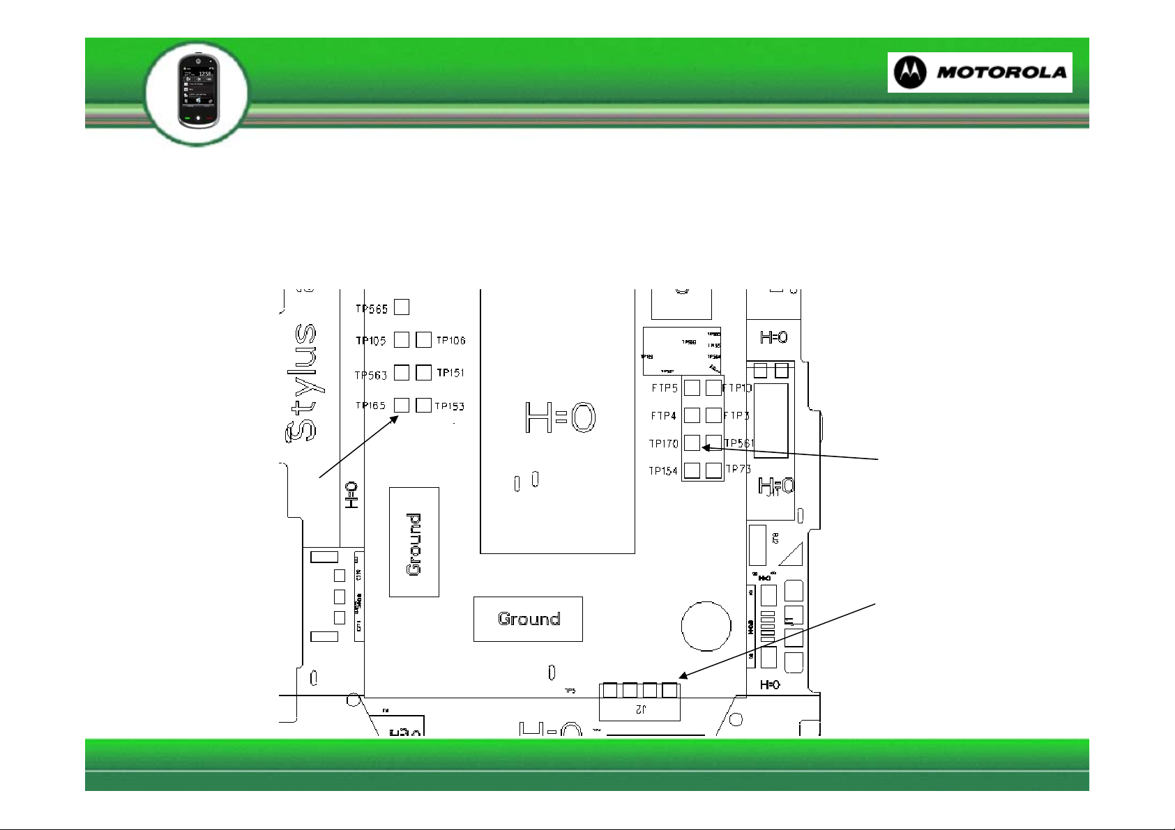
Can’t Power On (1)
1. Check the voltage of the Battery
Vbat (TP170) > 3.8V
2. Check the battery connector J2
Vbat (TP170)
N_KB_PWR_KE
Y
Service Engineeing & Optimization
Level 3 , Rev.1.0
Vbat (J2)
Page 4
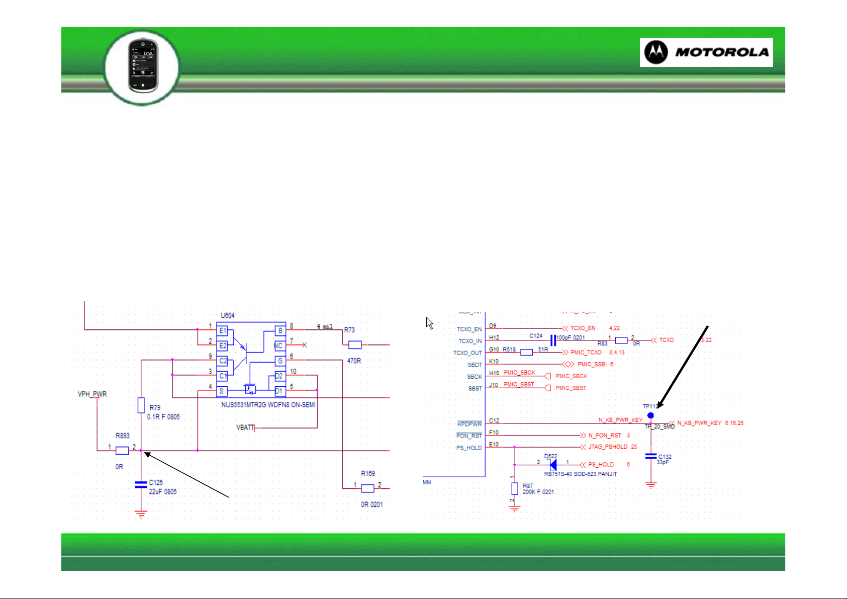
Can’t Power On (2)
3.Check the voltage of R79
R79 > 3.4V
4. Check the power-on key path
N_KB_PWR_KEY (TP165) > 2.6V
If N_KB_PWR_KEY is low, the unit will power on.
> 2.4 V
> 3.4 V
Service Engineeing & Optimization
Level 3 , Rev.1.0
Page 5
Can’t Power On (3)
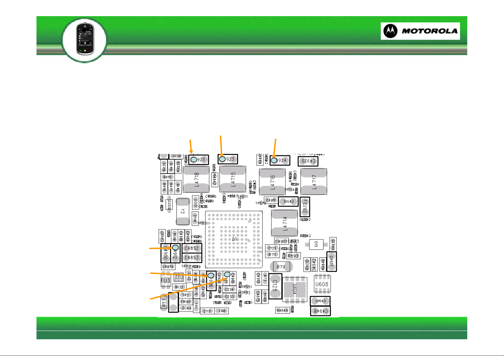
5. Check PM7540(U2) regulator voltage
A. VREG_MSMC1_1.2V on C4923
B. VREG_MSMC2_1.2V on C4924
C. VREG_MSME_1.8V on C4925
C
E
A
D.VREG_MSME2_2.8V on C4921
E. VREG_MSMP_2.6V on C4912
F. VREG_MSMA_2.6V on C4906
B
F
D
Service Engineeing & Optimization
Level 3 , Rev.1.0
Page 6
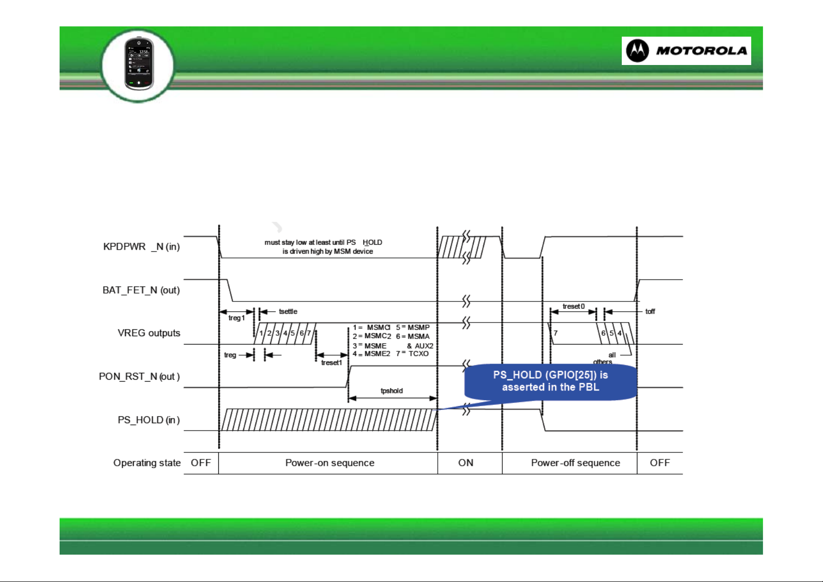
Can’t Power On (4)
6. Check Power On Sequence
After the voltage rails are brought up, PON_RST_N is asserted by
PM7540 IC, and then the MSM7200A IC asserts PS_HOLD signal.
– PS_HOLD should be high after power on (on D522)
Service Engineeing & Optimization
Level 3 , Rev.1.0
Page 7

Can’t Power On (5)
7. Try to check the external DDR and Nand Flash
1. External DDR check _ Check the External DDR by ram test tool
Pass=> The External DDR is workable
Fail => a) MSM7201A can find the memory
b) U3 is damaged
2. Flash check _ Dump the image from the damaged unit
Pass=> The External flash is workable
Fail => a) MSM7201A can find the flash
b) U3 is damaged
8. Redownload the SW
Try to redownload the SW if the main code image is damaged
Service Engineeing & Optimization
Level 3 , Rev.1.0
Page 8
SIM Card Not Found
1. Do the clean boot (Mater Clear)
2. Exam whether the contact between SIM and connector is ok
3. Check the Signal of SIM interface (VCC, RST ,and Clock)
USIM ,VCC =1.8V ; SIM= 1.8V / 2.85V
USIM SLOT
4. If the signal is abnormal ,please check U2.
VREG_UIM1
R249
10K 0201
UIM1_P_DATA12
21
R247
0R 0201
UIM1_P_RESET12
UIM1_P_CLK12
2 1
UIM1_DATA
C239
33pF 0201
2 1
2 1
33pF 0201
R245
0R 0201
R246
0R 0201
C296
VREG_UIM1
UIM1_RESET
UIM1_CLK
1
2
3
4
5
6
C297
33pF 0201
C288 1uF
J17
217-02000-04 6PIN 2.1H ACT
VCC
RST
CLK
GND
NC
I/O
Fix
Fix
Fix
Fix
Fix7Fix
C289 33pF
12
11
10
9
8
Service Engineeing & Optimization
Level 3 , Rev.1.0
Page 9
• White screen:
• Check LCM damage or not
• Check EMI filter (U4721) SMT
• Check panel voltage VDD 2.8V(C4921_1) & VDDIO 2.6V(C4918_1)
Display Abnormal
Service Engineeing & Optimization
Level 3 , Rev.1.0
Page 10
No Keypad Light
• Check keypad LED voltage VREG_5V(C259 pin2)
• Check LED damage or not
Service Engineeing & Optimization
Level 3 , Rev.1.0
Page 11

No LCM backlight
• No backlight:
1. LCM backlight damage
2. Measure R54 voltage: 15V
3. Backlight enable GPIO(Q1_2) pulled high 2.6V
Service Engineeing & Optimization
Level 3 , Rev.1.0
Page 12

Flash Light No Function
• Can’t turn on flash light:
1. Check flash LED (D523) SMT and damage or not
2. Check D523_pin1 voltage: 5V
3. R425_1 & R426_1 & R427_1 pulled to low when turn on flash
led.
Service Engineeing & Optimization
Level 3 , Rev.1.0
Page 13

Light Sensor No Function
– Check U39_2 voltage: 2.8V
– Check R685_1 signal pulled to low
– Measuring Vout voltage (U39_4) was change or not when light sensor
putting on different Lux environment.
Service Engineeing & Optimization
Level 3 , Rev.1.0
Page 14
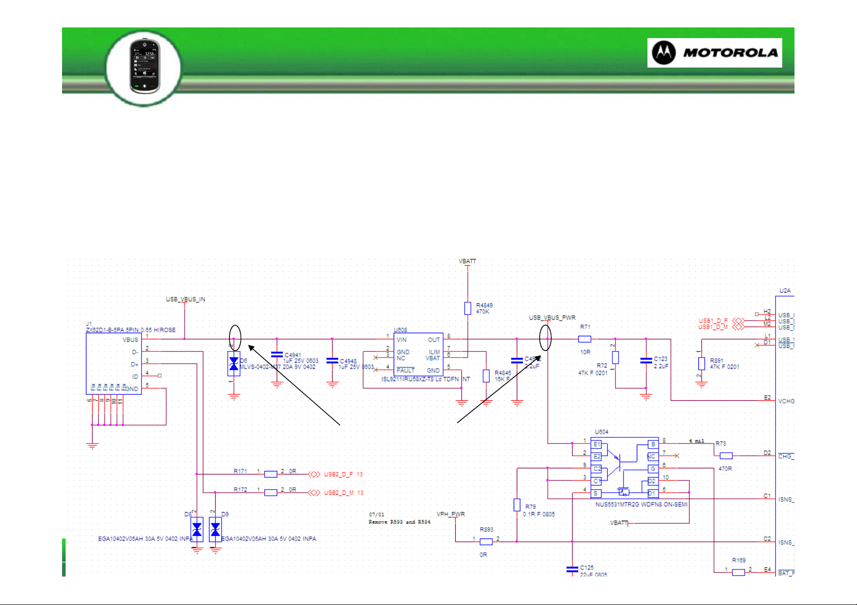
Cannot Charge (1)
1. Check the battery and the charger ; Only support BT-60 battery
2. Dial #06# to check the Charging status and the charging type
Power Source should be USB or Charger
Battery ID : Readable
If Power source is “No external power”, please check the charging path
Service Engineeing & Optimization
Level 3 , Rev.1.0
VBUS > 4.7V
Page 15
Cannot Charge (2)
• If Battery ID is not the readable , please check whether battery is
BT60 and contact to PIN3 OF J2
•
BATT_THERMAL_GAUGING
VREG_HKADC_2.85V
R93
J2
BATT+
DATA
THERM
BATT-
476150001 4P P2 MOLEX
4
3
2
1
n.m.
40mil
R147
100R
R92
VBATT
BATT_DATA_1
BATT_THERM 4
BATTERY CONNECTOR
BGND
Service Engineeing & Optimization
Level 3 , Rev.1.0
C197
39pF
n.m.
C198
39pF
Page 16
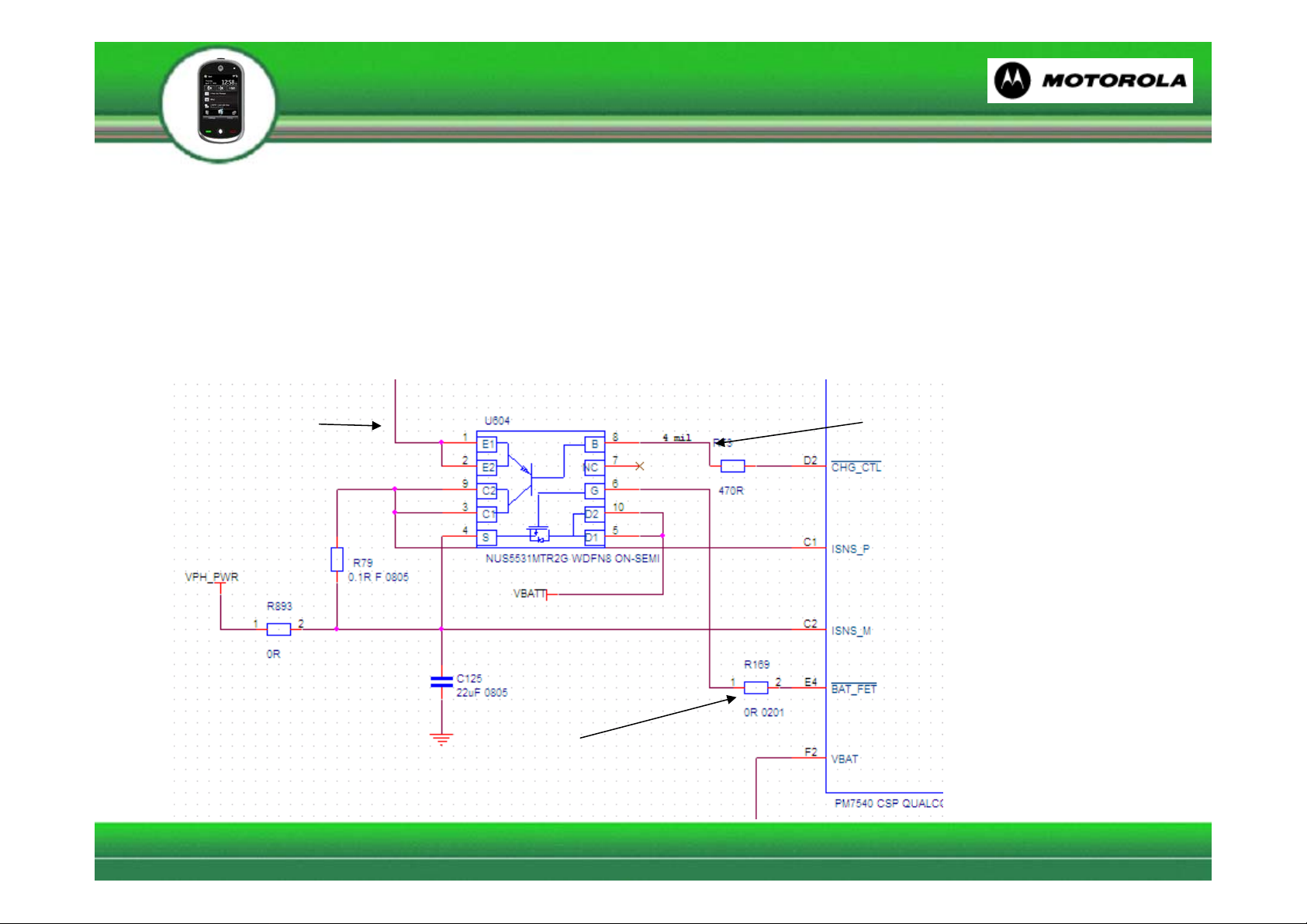
Cannot Charge (3)
3. Dial #77704# to check the gas gauge Status
AC Line : On (Has detect the charger)
Flag : Charging (The charger driver is active)
The current is minus, please check U604 circuit.
5V
Should be < 2V in charging
Service Engineeing & Optimization
Should be < 4.3V in charging
Level 3 , Rev.1.0
Page 17

Keypad No Function
1. Check S/B connector J13
Service Engineeing & Optimization
Level 3 , Rev.1.0
Page 18

Touch No Function
– Check TP damage or not
– Check assembly between main PCB and sub PCB
– Check J13 SMT
Service Engineeing & Optimization
Level 3 , Rev.1.0
Page 19

Jog Ball No Function
• 1. Check the magnet is at the correct position
• 2. Check the voltage (JB1-10 =2.85V)
• 3. Check the related circuit
Jog Left
Jog Up
Jog Right
U17
3
NC1
2
GND
1
NC
AN48840B
U18
3
NC1
2
GND
1
NC
AN48840B
U19
3
NC1
2
GND
1
NC
AN48840B
OUT
VCC
OUT
VCC
OUT
VCC
5
4
5
4
5
4
JOG_2.85V
C322 33pF 0201
Jog_RIGHT 6
GPIO_40 (2.6V)
D25
RCLAMP0521P
1 2
Jog_DOWN 6
GPIO_38 (2.6V)
D26
RCLAMP0521P
1 2
Jog_LEFT 6
GPIO_49 (2.6V)
D27
RCLAMP0521P
1 2
2.85V
Jog Down
Service Engineeing & Optimization
Level 3 , Rev.1.0
Magnet
Location
U20
3
NC1
2
GND
1
NC
AN48840B
OUT
VCC
5
4
C321
33pF 0201
Jog_UP 6
GPIO_90 (2.6V)
D28
RCLAMP0521P
1 2
Page 20

Can’t access the Micro SD Card
• If the T-Flash card can not be detected, check if the pin12 of J16 is
low. If not, check if J16 is OK.
• If pin12 of J16 is low when inserted, check if pin5 of J16 is 3V. If not,
check U2.
• Check if all the clock and data pins are normal. If not, check U1.
T-Flash Slot J16
Service Engineeing & Optimization
Level 3 , Rev.1.0
Page 21

Vibrator Out Of Control
• Remove the lower case and have the vibrator exposed, then retest.
• If retest OK after removing the case, reassemble and check if it is
interfered by the case.
• If retest still fail, check if pin1 of J11 is 5V. If not, check if U2 is
working normally.
• Check if there is PWM signal on pin2 of J11. If not, check if U2 is
working normally.
Service Engineeing & Optimization
Level 3 , Rev.1.0
Page 22

ActiveSync No Response
• 1. Do the clean boot (Master Clear)
• 2. Check the USB transceiver circuit while the unit has connected to
PC
Reset in High
Level
3.3V
Vbus > 4.3V
1.8V
19.2MHz
Service Engineeing & Optimization
Level 3 , Rev.1.0
Page 23

Earphone Malfunction (1)
• Check if the voltage at Pin 1 of R148 is logic low, if not, check the
audio jack J170 is OK and well-contacted with the main board.
• Using the oscilloscope to see if the waveform is visible at U10 or
U11, if visible at pin 4 but not pin 3, replace U10 or U11 with new
chips.
• If not visible at both pin 4 and pin 3, replace U1 with a new chip.
J170 Audio Jack
Service Engineeing & Optimization
Level 3 , Rev.1.0
Page 24

Earphone Malfunction (2)
Service Engineeing & Optimization
Level 3 , Rev.1.0
Page 25

Microphone Malfunction
• Check if the voltage at C113 is 2V, if not, replace U2 with a new chip.
• Check if the voltage at Pin 4 of J3 on sub board is 2V, if not, check if
the sub board is well-contacted with the main board, and if male and
female BTB connectors are robust and clean.
• Using the oscilloscope to see if the waveform is visible at R3 on sub
board, if not, replace the microphone.
Service Engineeing & Optimization
Level 3 , Rev.1.0
Page 26

Receiver Malfunction
• Check if J6 is blocked by anything.
• Using the oscilloscope to see if the waveform is visible at J6, if not,
replace U1 with a new chip.
• If the waveform is visible at J6, replace the receiver.
Receiver Pads J6
Service Engineeing & Optimization
Level 3 , Rev.1.0
Page 27

Speaker Malfunction (1)
• Using the oscilloscope to see if the waveform is visible at C233, if
not, replace U1 with a new chip.
• Using the oscilloscope to see if the waveform is visible at L15 & L14,
and the two waveforms should be out of phase with each other, if
not, replace U2 with a new chip.
• Using the oscilloscope to see if the waveform is visible at S1 & S2, If
yes, check if the sprints of S1 & S2 are distorted.
• If the sprints are in good shape, replace the speaker.
Service Engineeing & Optimization
Level 3 , Rev.1.0
Page 28

Speaker Malfunction (2)
Speaker Amp.
Service Engineeing & Optimization
Level 3 , Rev.1.0
Page 29

RTC failed
• 1, Do a power cycle with the unit
• 2. Check the Vcoin Voltage (BJ2)
• 3. Check the 32KHz oscillator
1V~ 3V
Service Engineeing & Optimization
Level 3 , Rev.1.0
32.768KHz
Page 30

Can’t Take Picture
• Can’t turn on:
• Check Camera damage or not
• Check camera module assembly
• I2C interface working normally (you could verify this by LCD
backlight level adjustment or turn on VGA camera)
• Check camera power when turn on ( R178_1.8V, R751_2.8V,
R752_2.6V )
• Check camera reset pin (R755) signal should pull high after turn on
camera
– AF no function:
• Check S7 SMT
• Check S7_pin3 signal from 2.6V to GND when you press the
capture key to the half.
• Check camera module AF pad short with shielding case or not.
– Capture key no function:
• Check S7 SMT
• Check S7_pin1 signal from 2.6V to GND when you press the
Service Engineeing & Optimization
Level 3 , Rev.1.0
capture key.
Page 31

3M Camera schematic and placement
Service Engineeing & Optimization
Level 3 , Rev.1.0
Page 32

Phone Hang Up
• 1. Dump the image
• 2. Copy the log in my device
• 3. Perform the clean boot
(press the end key and Jog ball before the power key in off mode)
4. If the unit can not into windows mobile, please redownload SW
image to the damaged unit.
5. If the issue isn’t solved ,please use Ram test tool to check U3.
If any error message , the U3 may be damaged.
Service Engineeing & Optimization
Level 3 , Rev.1.0
Page 33

Auto Power On
1. Please check the follow Power on event
a) Press the power key ->Pull N_KB_PWR_KEY to low (TP112)
On Page 4
b) Plug the USB charger /USB cable -> Detect VBUS
Page 14, Page 15 , Page 16
2. Check the SW2(power key) and the rubber with upper case
3. Try to Dump the image
4. Copy the Log in my device with Today mode to SW team for further
analysis
5. Redownload the new image to the damaged unit
Service Engineeing & Optimization
Level 3 , Rev.1.0
Page 34

Auto Power off
1. 1. Check the leakage current (< 0.4mA)
2. if the power off is triggered by the power key, the vibrator will active
for a while and then the unit is off.
=> Please check the SW2 power key.
3. If the unit is off without any vibration, please measure the power on
current (< 450mA)
=> Copy the Log in my device with Today mode to SW team for
further analysis
Service Engineeing & Optimization
Level 3 , Rev.1.0
Page 35

Can’t call out (1)
GSM
• Check the metal contact of antenna
• Try to make call
• Setup BS/MS parameter
• Set HP8960, operating mode: test mode, test function: BCH+TCH, cell power:-60dBm
• Set MS GSM900/850 ch62/189 PL=5; DCS/PCS ch699/ch661 PL=0
• Check transmitter path
– Check the I/Q path
• Use oscilloscope probe to touch red point and check waveform
Antenna pad
Service Engineeing & Optimization
Level 3 , Rev.1.0
Page 36

Can’t call out (2)
• Check transmitter path
– Check PA control signal
• Use oscilloscope probe to touch red point and check waveform
GSM
PA_EN
Service Engineeing & Optimization
Level 3 , Rev.1.0
PA_RAMP
Page 37

Can’t call out (3)
• Check transmitter path
– Check ASM control signal
• Use oscilloscope probe to touch red point and check control table
GSM
Service Engineeing & Optimization
Level 3 , Rev.1.0
Page 38

Can’t call out (4)
• Check transmitter path
– Check RF path power
GSM
• Use spectrum probe to touch red point and check output power in
spectrum analyzer
High band RF signal
Low band RF signal
~29dBm
Service Engineeing & Optimization
Level 3 , Rev.1.0
~30dBm
~33dBm
~10dBm
Page 39

• Check receiver path
– Check ASM control signal
• Use oscilloscope probe to touch red point and check control table
Can’t call out (5)
GSM
Service Engineeing & Optimization
Level 3 , Rev.1.0
Page 40

• Check receiver path
– Check RF signal power
Can’t call out (6)
GSM
• Use spectrum probe to touch red point and check output power in
spectrum analyzer
~ -65dBm
~ -65dBm
High band RF signal
Low band RF signal
~ -61dBm
Service Engineeing & Optimization
Level 3 , Rev.1.0
Page 41

Can’t call out (1)
WCDMA
• Check the metal contact of antenna
• Try to make call
• Setup BS/MS parameter
• Set MT8820, operating mode: test mode, cell power:-60dBm
• Set MS WCDMA BC1 ch9750, BC2 ch9400 and BC5 ch4183
• Check transmitter path
– Check the I/Q path
• Use oscilloscope probe to touch red point and check waveform
Antenna pad
Service Engineeing & Optimization
Level 3 , Rev.1.0
Page 42

Can’t call out (2)
• Check transmitter path
– Check PA control signal
• Use oscilloscope probe to touch red point and check control table
WCDMA
BC1
Service Engineeing & Optimization
Level 3 , Rev.1.0
BC1
BC5
BC2
BC2/5
Page 43

Can’t call out (3)
• Check transmitter path
– Check ASM control signal
• Use oscilloscope probe to touch red point and check control table
WCDMA
Service Engineeing & Optimization
Level 3 , Rev.1.0
Page 44

Can’t call out (4)
• Check transmitter path
– Check RF path power
WCDMA
~24dBm
~24dBm~24dBm
• Use spectrum probe to touch red point and check output power in
spectrum analyzer
~26dBm
~26dBm
~26dBm
BC1 RF signal
BC2 RF signal
BC5 RF signal
~1dBm
~1dBm
~23dBm
Service Engineeing & Optimization
Level 3 , Rev.1.0
Page 45

• Check receiver path
– Check ASM control signal
• Use oscilloscope probe to touch red point and check control table
Can’t call out (5)
WCDMA
Service Engineeing & Optimization
Level 3 , Rev.1.0
Page 46

• Check receiver path
– Check RF signal power
Can’t call out (6)
WCDMA
~ -65dBm
~ -65dBm~ -65dBm
• Use spectrum probe to touch red point and check output power in
spectrum analyzer
~ -68dBm~ -68dBm
~ -68dBm
BC1 RF signal
BC2 RF signal
BC5 RF signal
~ -61dBm
Service Engineeing & Optimization
Level 3 , Rev.1.0
Page 47

Bluetooth cannot turn on and test (1)
• Check the voltages: VBATT, VREG_MSMP_2.6V, and V1P8_WLAN
V1P8_WLAN
Test point: C302
Voltage: 1.8V
VREG_MSMP_2.6V
Test point: C1707
Voltage: 2.6V
VBATT
Test point: C1706
Voltage: 3.4~4.2V
Service Engineeing & Optimization
Level 3 , Rev.1.0
Page 48

Bluetooth cannot turn on and test (2)
• Check BT_REQ_OUT pin voltage.
• When BT_REQ_OUT pulls high, OSC will have 19.2MHz clock.
Test point: R1701 or R194
Voltage: 2.6V
When BT turns on or is working,
BT_REQ_OUT pin needs to
pull high.
Test point: R191 or C315
Clock voltage: 0.5~0.9Vpp
Clock frequency: 19.2MHz
Service Engineeing & Optimization
Level 3 , Rev.1.0
Page 49

Wi-Fi cannot turn on and test (1)
• Check the voltages: VBATT, VREG_MSMP_2.6V, V1P2_WLAN, and
V1P8_WLAN
V1P8_WLAN
Test point: C302
Voltage: 1.8V
V1P2_WLAN
Test point: C1704
Voltage: 1.2V
VREG_MSMP_2.6V
Test point: C1707
Voltage: 2.6V
VBATT
Test point: C1706
Voltage: 3.4~4.2V
Service Engineeing & Optimization
Level 3 , Rev.1.0
Page 50

Wi-Fi cannot turn on and test (2)
• Check the reference clock 26MHz.
Service Engineeing & Optimization
Level 3 , Rev.1.0
Test point: C318 or C317
Clock voltage: 0.5~0.9Vpp
Clock frequency: 26MHz
Page 51

Wi-Fi cannot turn on and test (3)
• Check the pin states of the module.
WOW
Test point: U16 pin 5
Clock voltage: 2.6V
SYS_RST_L
Test point: TP140
Clock voltage: 2.6V
CHIP_PWD_L
Test point: TP558
Clock voltage: 2.6V
Service Engineeing & Optimization
Level 3 , Rev.1.0
 Loading...