


3G A1000 TRAINING AID
1
Introduction:
It is the intent of this document to be used as a supplemental guide with the 3G training classes.
The information contained within this document is based on initial designs and theory of
functionality of 3G A1000 transceivers. It is also important to note that circuit designs are expected
to change in the future and certain information within this document will no longer be valid. All
information here in is subject to change and subsequent revisions of this document will be updated
as new design changes occur.
Future revisions of this document will elaborate further on efficient troubleshooting techniques.
Any questions, comments about this guide can be emailed to:
jerrypainter@motorola.com
June 3, 2004
Revision 1.0
MOTOROLA CONFIDENTIAL PROPRIETARY

3G A1000 TRAINING AID
2
MOTOROLA CONFIDENTIAL PROPRIETARY
3G A1000 TRAINING AID
3
MOTOROLA CONFIDENTIAL PROPRIETARY
3G A1000 TRAINING AID
4
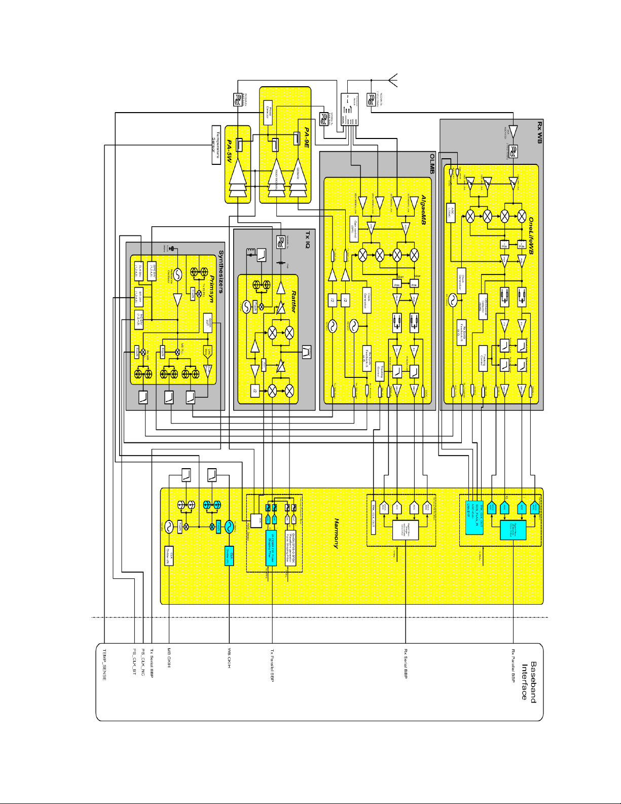
WCDMA Rx
Ceramic
Bandpass Filter
1
2
3
4
EGSM Rx
1805-1880
MHz
925-960
MHz
DCS Rx
1930-1990
MHz
PCS Rx
Antenna Switch
Diplexing
Networks
Balun/Matching
Networks
Harmonic
Filters
V1
ANT
RF
Gnd
WCDMA Tx
Ceramic
Bandpass
Filter
WCDMA Rx
Notch Filter
WCDMA Tx DCS/PCS Tx
EGSM Tx
EGSM Tx
DCS/PCS Tx
WCDMA Tx
GSM Rx
SAW Filters
DCS Rx
PCS Rx
EGSM Rx
TL3 TL4
TL5
TL1
TL2
FL6
FL1
FL7
FL2
FL3
FL4
FL8
FL9
FL10
FL11
FL12
FL13
FL14
V2
V3
V4
UMTS
WCDMA
LNA
GSM 1800
LNA
GSM 1900
LNA
GSM 900
LNA
GSM 900
PA
GSM 1800 /
GSM 1900
PA
WCDMA
2100
PA
TL6
TL7
TL0
WCDMA RX
The WCDMA Rx (downlink) frequency band is 2.11 - 2.17GHz and sensitivity @ ~106dBm.
FL1 Front End Module Part # 4889729N01
Overview:
The A1000 Front End Module (FEM) integrates a four position antenna switch controlled by
Harmony (U100), logic decoding and level shifting, diplexers, transmit harmonic filters, SAW
(Surface Acoustic Waveform) filters and matching components on a multi-layer ceramic module.
The module provides band selection and filtering between the EGSM, DCS, PCS and WCDMA
receive and transmit bands- to a single antenna port. The diplexing arrangement permits reception
MOTOROLA CONFIDENTIAL PROPRIETARY

3G A1000 TRAINING AID
5
of WCDMA signals in any switch position. This allows the phone, while in a GSM call in any band,
to detect signals from a WCDMA base station. The decision may then be made to hand over to the
WCDMA system. Similarly, EGSM base station signals can be detected while the phone is in a
WCDMA call to permit a handover decision from WCDMA to EGSM (This is not possible for base
station signals in the DCS and PCS bands.).
WCDMA Rx:
Signals received at the antenna between 2110 – 2170 MHz will see any path through the RF
switch as an open circuit due to the characteristics of FL1 through FL4. Consequently WCDMA Rx
signals will go through WCDMA Rx band-pass filter FL6 to the WCDMA receiver. Due to the outof-band impedance of FL6 and the phase rotation provided by TL2 and impedances inside the
Front End Module, signals in the other bands will see FL6 as an open circuit, preventing them from
reaching the WCDMA receiver.
WCDMA Tx:
Signals from the WCDMA transmitter pass through WCDMA Tx Band-pass Filter FL7, then through
diplexing network FL1, which isolates them from the EGSM Rx SAW filter while allowing them to
pass to the antenna when the switch is in position 1.
EGSM Rx:
With the switch in position 1, signals arriving at the antenna in the EGSM Rx band pass through
diplexing network FL1 to EGSM Rx SAW FL11. FL1 also provides attenuation at WCDMA Tx
frequencies to protect the SAW from transmit power. To a lesser degree, it also provides isolation
from transmit power when the switch is in position 3 (DCS/PCS Tx) and position 4 (EGSM Tx), as
the switch isolation alone may be insufficient to protect the SAW filter
PCS Rx:
With the switch in position 2, signals arriving at the antenna in the PCS Rx band pass through FL3
to PCS Rx SAW FL10. This position of the switch is not diplexed with a transmit path, so the
network may be simpler than the others. Like the other GSM receive paths, however, sufficient
attenuation at the other transmit frequencies is needed to protect the SAW from transmit power
unless the switch isolation is adequate.
DCS / PCS Tx:
When the switch is in position 3, signals from the DCS/PCS transmitter pass through Notch Filter
FL8 and diplexing network FL2 to the antenna port. The Tx harmonic filter is shown separately for
clarity, but the required harmonic attenuation would typically be provided by the stopband
characteristic of FL2. Notch filter FL8 attenuates thermal noise in the WCDMA Rx band coming
from the DCS/PCS transmitter, and forms a part of the overall diplexing network along with the
phase shift provided by TL4.
EGSM Tx:
Signals from the EGSM transmitter pass through diplexer FL4, which protects the DCS Rx SAW
filter from transmit power while allowing the EGSM Tx signal to pass to the antenna when the
switch is in position 4. The EGSM Tx harmonic filter is shown separately for clarity, but this
MOTOROLA CONFIDENTIAL PROPRIETARY

3G A1000 TRAINING AID
6
function would typically be provided by the stopband characteristic of FL4. TL5 represents the
transmission line length between the EGSM transmit coupler/detector and the EGSM Tx pin on the
Front End Module.
DCS Rx:
With the switch in position 4, signals arriving at the antenna in the DCS receive band pass through
diplexer FL4 to DCS Rx SAW FL9. FL4 also provides attenuation to protect the SAW from EGSM
transmit power, which shares the same switch position.
WCDMA RX
(Freq 2110-2170MHz)
U30 LNA Part # 5109944C61
The first IC in the WCDMA Rx line up is U30 (MC13820), which is a Low Noise Amplifier. The RX
frequency will be amplified and passed on to OneLife WB through FL300. The LNA is conrolled by
Harmony (U100) through two enable lines. MBC_EN1 enables gain for the LNA while MBC_EN2
enables the IC. Both lines can be probed at testpoints located near Harmony (TP120 and TP121).
U30 operates from the PCAP supply voltage VRF_RX_2_775.
U300 ONELife WB Part # 5109923D59
The ONElife WB is combination down converter/mixer and demodulator. VCO frequencies are
provided by PRIMSYN IC by control from Harmony. Control and programming are done through a
SPI interface from Harmony. Two supplies are required to power the IC, VRF_DIG_1.875V for SPI
lines and VRF_2.775V for RF portions.
Programming checks of the IC can be done by probing VCC_SF on C301 and C306. If this voltage
is not present ONELife is not operating. Testpoints are also available for AGC stages located near
Harmony (U100). These are TP 122-126.
MOTOROLA CONFIDENTIAL PROPRIETARY
3G A1000 TRAINING AID
7
OneLife
WCDMA
WCD
LN
Mix
Mix1-IFIF1-PMOutp
Buff
Bi-2-Bi-
2-
C_mo
BB
Tracking
Mix
Tracking
PM
AGC
Trk_C
(15.36M
AG
VC
/
/
Syn_F
Syn_F
VCO_Tu
Jon
Jan 13,
Analog
Analog
Analog
Analog
DCOC_
DCOC_
DCOC_
DCOC_
I2+Q2-Compar
SOS
SOS
RF
2110-
SOS
90de
MOTOROLA CONFIDENTIAL PROPRIETARY

3G A1000 TRAINING AID
8
PA-9E
Ven,det
Vmode
VenH
VenL
Algae-MB
RX_EN
MB_RX_V CO _EN
MB_ASPI_CLK
MB_ASPI_DATA
MB_ASPI_CE
MB_EXC_ EN
PA-5W
Vld
Ven
Front-end
Module
V1
V2
OneLife-WB
SPI_CLK
SPI_DATA_IN
SPI_CE
Rx_En
VCO_En
SF_En
HARMONY
System Clocks
Syn_WB_Clk_Out
Syn_MB_Clk_Out
Tx_Ser_Frame_Out
Tx_Ser_Clk_Out
Tx_Ser_Data_In
Rx_Ser_Frame_Out
Rx_Ser_Clk_Out
Rx_Ser_Data_Out
Serial BBP
Parallel BBP
Tx_Par_Frame_In
Tx_Par_Data_In[7-0]
Rx_Par_Frame_Out
Rx_Par_Data_Out[7-2]
Syn_Par_Clk_Out
Rx_MB_Slot_In
Rx_MB_Acq_In
Rx_MB_On_In
Rx_WB_Slot_In
Rx_WB_On_In
Rx_WB_Acq_In
Tx_Start_In
Tx_Ramp_In
Tx_Prekey_In
Tx_Slot_In
Sequence Manager Triggers
Tx_AOC_Up_Dwn
RstB_In
Spi_Clk_In_0
Spi_Data_In_0
Spi_Data_Out_0
SPI
Spi_CE_In_0
Spi_Clk_In_1
Spi_Data_In_1
Spi_CE_In_1
Rx Aux SPI
RX_Aspi_Clk_Out
RX_Aspi_Data_Out
RX_Aspi_CE_Out
Tx Aux SPI
TX_Aspi_Clk_Out
TX_Aspi_Data_Out
TX_Aspi_CE_Out
GPO23
GPO22
GPO21
GPO20
GPO19
GPO18
GPO17
GPO16
GPO15
GPO14
GPO13
GPO12
GPO11
GPO10
GPO9
GPO8
GPO7
GPO6
GPO5
GPO4
GPO3
GPO2
GPO1
GPO0
TX Seq Mgr
RX MB Seq Mgr
RX WB Seq Mgr
Rattler
TX-EN
VCO-EN
SPI-CLK
SPI-DATA
SPI-CE
SW_VCO_EN
TX_EN
MB_EXC_EN
FEM_V1
TX_W B_EN
LB_EN
HB_EN
5W_VLD
TX_EN_2V7
FEM_V4
9E_VMODE
TEMP_SENS E_EN
WB_RX_E N
SW_VCO_EN
TX_EN
MB_EXC_EN
LB_EN
HB_EN
5W_VLD
TX_EN_2V7
9E_VMODE
MB_RX_EN
TX_W B_EN
HAR_WB_RX_ACQ
HAR_TX_SLOT
HAR_TX_PREKEY
HAR_WB_RX_SLOT
HAR_MB_RX_ACQ
HAR_MB_RX_SLOT
HAR_MB_RX_ON
WB_CKIH
MB_CKIH
SER_TX_DATA
SER_RX_FRAME
SER_RX_CLK
SER_RX_DAT A
PAR_TX_FRAME
PAR_TX_DATA (7:0)
PAR_RX_FRAME
PAR_RX_DAT A (7:2)
PAR_TRX_CLK
HAR_MB_RX_SLOT
HAR_MB_RX_ACQ
HAR_MB_RX_ON
HAR_WB_RX_SLOT
HAR_WB_RX_ACQ
HAR_WB_RX_ON
TX_RAMP
HAR_TX_PREKEY
HAR_TX_SLOT
WB_VCO_SF_EN
MB_RX_VCO_EN
MB_RX_VCO_EN
WB_VCO_SF_EN
WB_RX_E N
SPIWB_CLK
SPIWB_DW
SPIWB_DR
HAR_SPIWB_CE
SPIWB_CLK
SPIWB_DW
SPIWB_DR
SPIMB_CLK
SPIMB_DW
HAR_SPIMB_CE
SPIMB_CLK
SPIMB_DW
SPIMB_DR
HAR_SPIWB_CE
PS_SPIWB_CE
PS_SPIMB_CE
WB_SPIWB_CE
HAR_SPIMB_CE
SPIWB
SPIWB
SPIMB
SPIMB
SPIMB
PS_SPIMB_CE
SPIWB
PS_SPIWB_CE
WB_SPIWB_CE
SPIWB
HAR_RESET B
HAR_RESET B
STBY_WB
HAR_RESET B (E1000) or PCAP_RESET B (A1000)
STBY_WB
HAR_WB_RX_ON
DMCS
AOC_PWR_UP_DN
AOC_PWR_UP_DN
SER_TX_DATA
SER_TX_CLK
DMCS
SER_TX_CLK
PrimSyn
SPIWB_CLK
TXCLK
SPIWB_DATA
SPIWB_CE
SPIMB_CLK
SPIMB_DATA
SPIMB_CE
SDTX
TXRAMP
RESETB
STBY_WB
POG
MQSPI1_CK1
MQSPI1_DI1
MQSPI
MQSPI1_CK2
MQSPI1_DI2
MQSPI1_DO2
MQSPI1_SPI_CS_0
MQSPI2_SPI_CS_1 (MQSPI1_SPI_CS_1 pin)
MQSPI1_SPI_CS_2
MQSPI2_CS[3] (GPIO17 pin)
GPIO18
MQSPI1_CS[5] (GPIO19 pin)
L1T1_TOUT_1_6
L1T1_TOUT_1_5
L1T_1/2
L1T1_TOUT_1_4
L1T1_TOUT_1_3 [WB] / L1T1_TOUT_2_11 [MB]
L1T1_TOUT_1_2 [WB] / L1T1_TOUT_2_10 [MB]
L1T1_TOUT_1_1 [WB] / L1T1_TOUT_2_9 [MB]
L1T1_TOUT_1_0
L1T1_TOUT_2_6 (L1T1_TOUT_1_14 pin)
L1T1_TOUT_2_5 (L1T1_TOUT_1_13 pin)
L1T1_TOUT_2_4 (L1T1_TOUT_1_12 pin)
L1T1_TOUT_2_3 (L1T1_TOUT_1_11 pin)
L1T1_TOUT_2_2 (L1T1_TOUT_1_10 pin)
L1T1_TOUT_2_1 (L1T1_TOUT_1_9 pin)
DSM_1/2
STBY1 [ = (STBY1 & STB Y1_en) & (ST BY1 & S TBY 1_en) ]
CLKSEL1
STBY2
CLKSEL2 (A_SC0 pin)
Parallel BBP
TX_FRAME
TX_DATA_[7-0]
RX_FRAME
RX_DATA_[7-2]
CLK_CHIPX8
Serial BBP
BBP_TX_FRAME
BBP_TX_CLK
BBP_TX_DATA
BBP_RX_FRAME
BBP_RX_CLK
BBP_RX_DATA
GPIO
GPIO13
GPIO22
CKIH
CKIH1
CKIH2
MQSPI1_DO1
HELEN - APPLICATION PROCESSOR
PS_CLK_E N
PS_CLK_B T
PCAP - POWER MANAGEMENT IC
TEMP_SENS E (Analog signal )
BB/RF
Interface
1.875 V digital l ogic
2.775 V digital l ogic
Analog s ignal
STBY_MB
STBY_MB
STBY_MB
Syn_Standby_In_<1>
TEMP SENSOR
TEMP_SENS E_EN
MB_RX_EN
STBY_WB
STBY_MB
GPIO2
CLK_OUT
REF_IN
PS_CLK_NC
BLUETOOTH MODULE
FEM_V2
FEM_V4
FEM_V1
V4
V3
FEM_V3
WB_VCO_SF_EN
MB_RX_VCO_EN
VCO_EN_WB
VCO_EN_MB
PS_CLK_OUT
RA_BIAS_MIXER
Syn_Standby_In_<0>
BIAS_MIXER
AD_TRIG
Vcc
AD_TRIG
PCAP_RES ETB
WCSP
PA_ENABLE
FEM_V2
FEM_V3
TX_RAMP
U100 HARMONY Part #
5188450M23
Overview:
The HARMONY (U100) handles the backend processing of the WCDMA in phase (WB_RXI,
WB_RXIX) and quadrature (WB_RXQ, WB_RXQX) signals from the demodulator (ONELife WB
U300). The HARMONY performs an analog to digital conversion of gain, phase and DC offset
correction of the RX data and sends it to POG via data lines (BBIF_OUT_D0 thru BBIF_OUT_D9).
SPI Lines:
The HARMONY has two sets of SPI interfaces; one set is for handling the control interface for the
transceiver (AUXSPI lines) and ones for interfacing with POG (SPI lines). Further, all SPI interface
is generated from POG and written to HARMONY or parsed through to the ONELife WB (U300)
part.
MOTOROLA CONFIDENTIAL PROPRIETARY

3G A1000 TRAINING AID
9
BaseBand Interface (BBIF):
The BBIF is the transmit and receive data path for transferring digitally sampled I / Q data to and
from the POG. The transmit half of the interface runs at the chip rate, supplying 8-bit I / Q pairs at
a 3.84MHz rate. An FIR in the HARMONY filters and un-samples the transmit data to 8x
(interleaved) the chip rate to be applied t the transmit DACs. The receive path of the interface
transmits I / Q samples at 4x the chip rate, or 15.36MHz, which is supplied by the PRIMSYN.
Layer One Timing:
Layer one timing signals control the functionality of the RF section of the transceiver relative to
the air interface. There are three signals defined on each transmit and receive section of the
transceiver. TX_PRE_KEY and RX_ON are asserted before the need to receive or transmit in
order to launch the necessary sequence of events to warm up the required functional blocks.
TX_RAMP and RX_AQUIRE are asserted when actual transmission and reception are to begin.
RX_SLOT and TX_SLOT are used during continuous transmission and reception to trigger events
that must be aligned with slot boundaries. It’s important to reiterate, the TX_RAMP directly
corresponds to the PA turning on and RX_AQUIRE corresponds to data being sent to the POG.
Block Diagram:
MOTOROLA CONFIDENTIAL PROPRIETARY

3G A1000 TRAINING AID
10
MOTOROLA CONFIDENTIAL PROPRIETARY

3G A1000 TRAINING AID
11
WCDMA TX
The WCDMA TX (uplink) frequency band is 1920-1980 MHz @ 1/4 watt / 24dBm.
U100 HARMONY Part# 5188450M23
Overview:
The HARMONY (U100) generates WCDMA in phase (WB_TXI, WB_TXIX) and quadrature
(WB_TXQ, WB_TXQX) signal lines from the POG. The HARMONY will perform a digital to analog
conversion of the digitally sampled I /Q from the POG via data lines from the POG (U1000) via data
lines (BBIF_IN_D0 thru BBIF_IN_D9).
SPI Lines:
The HARMONY has two sets of SPI interfaces; one set is for handling the control interface for the
transceiver (AUXSPI lines) and ones for interfacing with POG (SPI lines). ). Further, all SPI
interface is generated from POG and written to HARMONY or parsed through to the RATTLER
(U200) part.
BaseBand Interface (BBIF):
The BBIF is the transmit and receive data path for transferring digitally sampled I / Q data to and
from the POG. The transmit half of the interface (data sent from Tx to POG) runs at the chip rate,
supplying 8-bit I / Q pairs at a 3.84MHz rate. An FIR in the HARMONY filters and un-samples the
transmit data to 8x the chip rate to be applied the transmit DACs. The receive path of the interface
(data sent to HARMONY from the POG) transmits I / Q samples at 15.36MHz.
Layer One Timing:
Layer one timing signals control the functionality of the RF section of the transceiver relative to
the air interface. There are three signals defined on each transmit and receive section of the
transceiver. TX_PRE_KEY and RX_ON are asserted before the need to receive or transmit in
order to launch the necessary sequence of events to warm up the required functional blocks.
TX_RAMP and RX_AQUIRE are asserted when actual transmission and reception are to begin.
RX_SLOT and TX_SLOT are used during continuous transmission and reception to trigger events
that must be aligned with slot boundaries.
U200 RATTLER Part# 5188450M21
Overview:
The RATTLER receives the differential I/Q BaseBand from Harmony (U100). It contains an
onboard VCO to generate transmit frequencies of 1920-1980 Mhz as well as a variable attenuator
controlled by a VGC line. The synthesizer is programmable through a SPI bus from HARMONY
(U100). If transmit frequency does not change from 1950 MHz, then SPI programming is not
occurring. This a is a default frequency for RATTLER. This IC operates from the supply voltage
VRF_TX_2_775V.
MOTOROLA CONFIDENTIAL PROPRIETARY

3G A1000 TRAINING AID
12
REF_15.36MHz:
The 15.36MHz frequency is supplied from PRIMSYN (U500) and is used throughout A1000 as a
reference.
.
U400 PA 5W Part # 518955N02
Overview:
U400 is a three-stage power amplifier handling the band of WCDMA Tx frequencies between 1920
– 1980MHz. The nominal expected maximum gain is ~30dB.
Gain Control:
HARMONY controls the RF biasing of the amplifier at pins #4 (VBA1) and #5 (VBA2) with a
control range of 0 – 2.5v. HARMONY also controls pin #12 (VLD) for PA load switching. PA load
switching in WCDMA is vitally important to conserve battery life and to avoid unnecessary radio
interference with base stations. When VLD is at a low state (0v), the transmitter is in high power
mode, consuming higher current but with overall better PA performance. When VLD is at a high
state, the transmitter is in low power mode, consuming less current with overall poor PA
performance. In theory, as the TX power level increases or decreases beyond a certain power
threshold, VLD is enabled or disabled. As TX power decreases (as requested from a base station)
down to ~14.5dBm, VLD will switch high. If TX power is requested to increase beyond ~19dBm,
VLD is switched low.
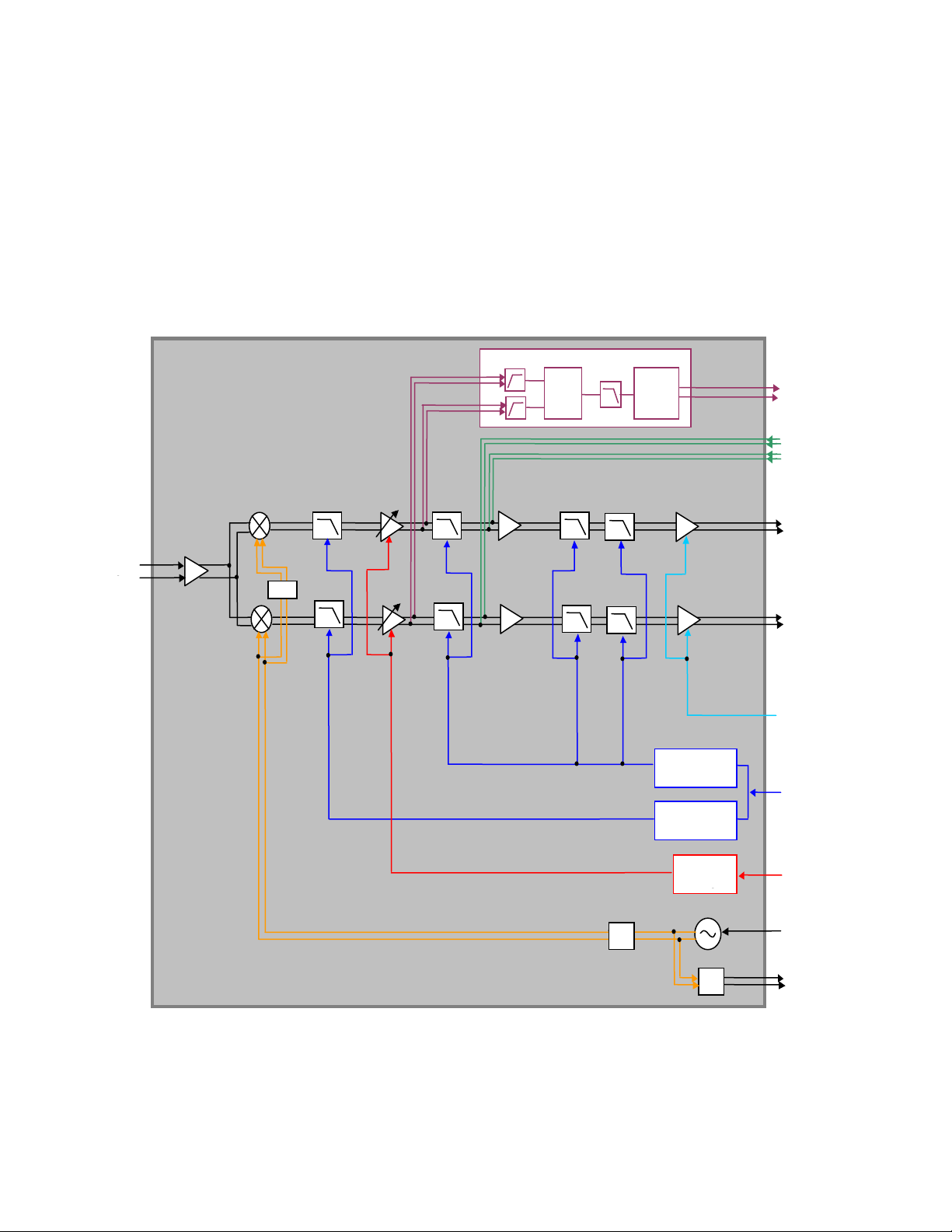
U500 PRIMSYN (Synthesizer) Part # 5188450M26
Overview:
The PRIMSYN IC provides RF frequencies for WCDMA RX as well as GSM TX and RX with
feedback lines for each.. It also provides the necessary reference clocks for WCDMA and GSM,
15.36 MHz and 13 MHz respectively. Source is a 26 MHz crystal oscillator. Power suppies from
PCAP include VRF_HV_5V for charge pumps, VRF_DIG_1.875V for logics, and VRF_RX_2.775V
for oscillators.
MOTOROLA CONFIDENTIAL PROPRIETARY

3G A1000 TRAINING AID
13
MOTOROLA CONFIDENTIAL PROPRIETARY
3G A1000 TRAINING AID
14
MOTOROLA CONFIDENTIAL PROPRIETARY

3G A1000 TRAINING AID
15
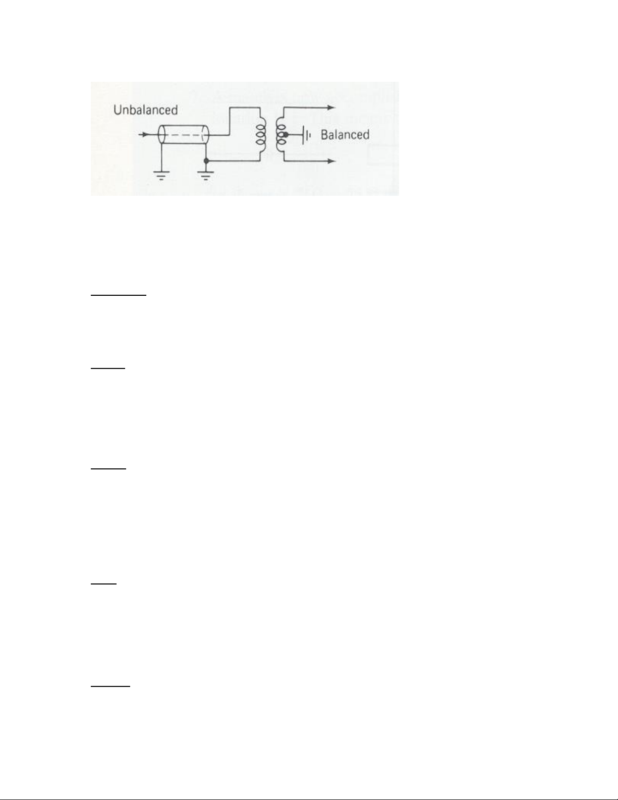
EGSM, PCS and DCS RX:
The EGSM Rx (reverse) frequency is 925 - 960MHz, DCS is 1805 – 1880MHz and PCS is 1930 –
1990MHz. The reference sensitivity level for the receivers is ~ - 102dBm.
T610, T620 and T630
Overview:
The EGSM, PCS and DCS signals must first pass through baluns before reaching the ALGAE IC.
Since the ALGAE expects differential inputs, the baluns will provide this. Baluns provide the
change from an unbalanced to a balanced line condition. By directly connecting to lines together, a
possibility might arise where one line might ground a signal and impair the operation of a circuit.
This situation is solved through the use of an un-balanced to balanced transformer, a balun.
Expected nominal losses is ~. 5 – 1.0dBm.
MOTOROLA CONFIDENTIAL PROPRIETARY
3G A1000 TRAINING AID
16
U600 ALGAE Part # 5109923D61
Overview:
The first IC in the EGSM, DCS, and PCS RX line up is U600 ALGAE, which is an LNA, VCO,
and down converter mixer. The ALGAE operates from a PCAP supply voltage of
VRF_RX_2.775V.
LNAs:
ALGAE is comprised of four low noise amplifiers (three of which are used) with two quadrature
mixer paths for use in receive GSM 900 (925– 960MHz), DCS (1805–1880MHz), and PCS (1930–
1990MHz) frequency bands, all SPI programmable from HARMONY (U100). The SYNTH_FB
signal or prescaler is fed back to the PRIMSYN (U500) prescaler input. Although the frequency will
be dependent of the channel selected, the amplitude signal is ~30dBm.
VCOs:
ALGAE contains three fully contained VCOs which operate at 3476-3980 MHz. These VCOs are
internally divided to provide precise quadrature down conversion for the three frequency bands.
The input signal RX_TUNE from the PRIMSYN selects the VCO frequency. The tune range is .5 –
4.5V. The VCO frequencies for the three technologies are: DCS/GSM 722MHz-768MHz and PCS
772MHz-796MHz. The calculation for the VCO frequency is Rx frequency x [4 (GSM/DCS) or x 2
(PCS]) / 5 @ ~-20/25dBm.
AGC:
The AGC is provided by four separate amplifiers, one for each LNA (three of which are used).
The amplifier gain control uses a linearizer to provide a response that is linear in dB/V. The AGC
linearizer is designed to accept a voltage input to provide the necessary attentuation slope that is
phaseable through a 6-bit DAC via the SPI lines (MB_ASPI_DATA, MB_ASPI_CLK, and
MB_ASPI_CE).
I and Q
The output signals MB_RX_I / IX and MB_RX_Q / QX are @ ~100KHz IF value for the Very Low
IF. The input pin, MB_RX_EN controls the on / off state of the receiver and the PLL circuits. For
MOTOROLA CONFIDENTIAL PROPRIETARY

3G A1000 TRAINING AID
17
input amplitude at the antenna of –50 to –40dBm the expected nominal output should be an AC
rms peak-to-peak voltage of ~4.5 - 14mV.
Block Diagram:
U100 HARMONY Part #5188450M23
Overview:
The HARMONY (U100) handles the backend processing for the EGSM, DCS and PCS
(MB_RX_I, MB_RX_I_X, MB_RX_Q, and MB_RX_Q_X) signal lines from ALGAE. Simply, the
HARMONY performs an analog to digital conversion of I /Q and sends it to the data to the board
processor (POG) via the BFSR, BCLKR, and BDR.
MOTOROLA CONFIDENTIAL PROPRIETARY

3G A1000 TRAINING AID
18
EGSM, PCS and DCS TX:
The EGSM Tx (forward) frequency band is 880 - 915MHz @ 2 watts / 33dBm. DCS is 1710 –
1785MHz and PCS is 1850 – 1910 MHz @ 1 watt / 30dBm.
MOTOROLA CONFIDENTIAL PROPRIETARY

3G A1000 TRAINING AID
19
U500 PRIMSYN (Synthesizer)Part # 5188450M26
Overview:
The PRIMSYN (U500) handles the backend processing for the EGSM, DCS and PCS. TX data is
sent from POG through BBP_TX_DATA to PRIMSYN (U500) through SD_TX pin and directly
modulated before being passed on to the ALGAE IC (U600).
BaseBand Interface:
The PRIMSYN receives SSI TX data at DMCS (digital input to start Tx modulation), TXCLK (clock
for serial transfer) and SDTX (serial Tx data) from POG. This data pattern input to a fractional N
synthesizer with a 24-bit resolution. For EGSM the synthesizer output is 880 – 915MHz, DCS is
1710 – 1785MHz with GMSK modulation and is directly amplified to the transmitter output.
SPI:
The PRIMSYN uses a SPI interfaces to communicate with POG..
Synthesizer / Tank Circuit:
The reference oscillator is a free running 26MHz crystal. AFC is provided through the SPI bus as
a programming offset to the fractional N division system. Since the 26MHz crystal is not locked to
the AFC, a second fractional divider system is necessary to derive an accurate 200KHz system
reference.
U600 ALGAE Part # 5109923D61
PLL:
A second programmable digital LO based on a look up ROM generates digital quadrature
oscillation with programmable gain / phase correction to digitally down convert the I/Q signals to
BaseBand through four quadrature mixers that provide image rejection of adjacent / alternate
channels. The PLL operates at a frequency of 13MHz.
MOTOROLA CONFIDENTIAL PROPRIETARY

20
Overview:
3G A1000 TRAINING AID
U800 PA DURANGO-9E
U800 is a tri-band PA module that operates in EGSM, DCS and PCS bands. The nominal
expected maximum gain is ~30dB. The VDET (output) is the RF feedback along the DC reference
V_REF_DET (output) are used in backend processing by the HARMONY.
VBA:
VBA_1 and VBA_2 are inputs from HARMONY that controls the PA output. The voltage applied at
the pin is proportionally related to the output power of the PA, as the voltage increases the gain or
power level increases.
POWER DETECTION:
The power detector is internal to the PA and is shared among all GSM bands as well as WCDMA.
CPIN connects WCDMA TX to the power detector
MOTOROLA CONFIDENTIAL PROPRIETARY

3G A1000 TRAINING AID
21
Dakota Colorado comparison
The Colorado chipset reduces the number of parts required to perform the same
operations as the Dakota. The detailed differences will be listed here.
HARMONY
Harmony is basically a combination of ICs from the Dakota platform.
In Dakota, the MAGIC IC had direct SPI control from POG and controlled the GSM
receive and transmit functions. Harmony Lite handled WCDMA receive and transmit
Now only Harmony has direct SPI control from POG. Harmony in the Colorado
platform is used for control of all receive and transmit function of both GSM and
WCDMA through AuxSPI(ASPI).
REF OSC
The Colorado platform now generates all Reference Frequencies from one oscillator. A
26 MHz crystal is used by the PRIMSYN IC to generate the 15.36 MHz and 13 MHz
reference clocks.
In Dakota, this was accomplished by two separate crystals and two separate
ICs(Harmony Lite and MAGIC).
GSM RX and TX
Receive and transmit functions in Colorado are handled by one IC, ALGAE with VCO
frequencies provided by PRIMSYN.
Dakota has three separate ICs to perform the same functions, LIFE and MAGIC with an
external PLL and VCO.
WCDMA RX and TX
Colorado employs a similar line up to Dakota for receive and transmit but the ICs have
changed. An external LNA is still used for the receiver which is then passed on to a
demodulator(ONE LIFE IC) and eventually to Harmony.
Colorado transmit is also similar. Starting with Harmony, the I and Q are sent to a
modulation IC known as Rattler. This IC has an internal VCO which is used to generate
MOTOROLA CONFIDENTIAL PROPRIETARY

3G A1000 TRAINING AID
22
transmit frequencies. It also contains the attenuator for output power. This attenuator in
Dakota was separate from the modulator.
RF DETECT
In Dakota, RF detect was handled separately for GSM and WCDMA. GSM was internal
to the PA. WCDMA had an external RF detect IC. Both were controlled by Harmony
Lite.
In Colorado, RF detect in conducted by the detector in the GSM PA for both GSM and
the WCDMA transmitters. Control is by Harmony.
.
MOTOROLA CONFIDENTIAL PROPRIETARY
 Loading...