

Page 1

APPLICANT: MOTOROLA EQUIPMENT TYPE: ABZ89FC5798-P
INSTRUCTION MANUALS
Excerpts from the instruction and service manuals for this base radio are available and have been included as part
of the filing package in the form of an e le ctronic pdf document.
Upon request, published and/or printed manuals will be sent to the commission and/or telecommunication
certification body (TCB). All of the descriptions and schematics included this filing package are up to date.
EXHIBIT 8
Page 2

APPLICANT: MOTOROLA INC. EQUIPMENT TYPE: ABZ89FC5798-P
TUNE-UP PROCEDURE
There is no field tune-up procedure. All adjustments are software controlled and are pre-set at the factory. Certain
station operating parameters can be changed via man-machine interface (MMI) commands, within predetermined
limits. Examples include transmit / receiver operating frequencies and power level.
EXHIBIT 9
Page 3

Technical Manual
iDEN
Enhanced Base Transceiver System (EBTS)
Volume 2 of 3
Base Radios
68P80801E35-E
16-June-06
RF SUB-SYSTEM
Page 4

Notice to Users
No part of this publication, or any software included with it, may be reproduced, stored in a retrieval system, or transmitted in any
form or by any means, including but not limited to, photocopying, electronic, mechanical, recording or otherwise, without the
express prior written permission of the copyright holder. Motorola, Inc. provides this document “AS IS” without warranty of any kind,
either expressed or implied, including but not limited to, the implied warranties of merchantability and fitness for a particular
purpose. Motorola reserves the rights to make changes or improvements in the equipment, software, or specifications described
in this document at any time without notice. These changes will be incorporated in new releases of this document.
Computer Software Copyrights
rd
The Motorola and 3
Motorola and other 3
States and other countries preserve for Motorola and other 3
programs, including the exclusive right to copy or reproduce in any form of the copyrighted computer program. Accordingly, any
copyrighted Motorola or other 3
instruction manual may not be copied, reverse engineered, or reproduced in any manner without the express prior written
permission of Motorola or the 3
either directly or by implication, estoppel, or otherwise, any license under the copyrights, patents or patent applications of Motorola
or other 3
rd
Party supplied SW, except for the normal non-exclusive, royalty free license to use that arises by operation of law in
Party supplied Software (“SW”) products described in this instruction manual may include copyrighted
rd
Party supplied computer programs stored in semiconductor memories or other media. Laws in the United
rd
Party supplied SW computer programs contained in the Motorola products described in this
rd
Party SW supplier. Furthermore, the purchase of Motorola products shall not be deemed to grant,
rd
Party supplied SW certain exclusive rights for copyrighted computer
the sale of a product.
Use and Disclosure Restrictions
The software described in this document is the property of Motorola, Inc. It is furnished under a duly executed license agreement
and may be used and/or disclosed only in accordance with the terms of the said agreement.
The software and documentation contained in this publication are copyrighted materials. Making unauthorized copies is prohibited
by law. No part of the software or documentation may be reproduced, transmitted, transcribed, stored in a retrieval system, or
translated into any language or computer language, in any form or by any means, without the express prior written permission of
Motorola, Inc.
Trademarks
MOTOROLA, the Stylized M Logo, iDEN, and Message Mail are trademarks or registered trademarks of Motorola, Inc. in the United
States and other countries.
All other product or services mentioned in this document are identified by the trademarks or service marks of their respective
companies or organizations, and Motorola, Inc. disclaims any responsibility for specifying their ownership. Any such marks are
used in an editorial manner, to the benefit of the owner, with no intention of infringement.
While reasonable efforts have been made to assure the accuracy of this document, this document may contain technical or
typographical errors or omissions. Motorola, Inc. and its subsidiaries and affiliates disclaim responsibility for any labor,
materials, or costs incurred by any person or party as a result of using this document. Motorola, Inc., any of its subsidiaries or
affiliates shall not be liable for any damages (including, but not limited to, consequential, indirect, incidental, or special damages
or loss of profits or data) even if they were foreseeable and Motorola has been informed of their potential occurrence, arising
out of or in connection with this document or its use. Motorola, Inc. reserves the right to make changes without notice to any
products or services described herein and reserves the right to make changes from time to time in content of this document
and substitute the new document therefor, with no obligation to notify any person or party of such changes or substitutions.
© 2006 - Motorola, Inc. All Rights Reserved REV 12/15/06
Contact Information
Motorola, Inc.
Networks business
1501 Shure Dr.
Arlington Heights, IL 60004
U.S.A
SPECIFICATIONS ARE SUBJECT TO CHANGE WITHOUT NOTICE.
Page 5

About This Volume
Volume 2 of the Enhanced Base Transceiver System (EBTS) manual, Base
Radios, provides the experienced service technician with an overview of the
EBTS operation and functions, and contains information regarding the 800
MHz, 900 MHz, 800/900 MHz QUAD Channel, and 800/900 MHz QUAD+2
Channel base radios.
The EBTS has three major components:
■ Generation 3 Site Controller (Gen 3 SC) or integrated Site Controller (iSC)
■ Base Radios (BRs)
■ RF Distribution System (RFDS)
Installation and testing is described in Volume 1, System Installation and
Testing, and RFDS are described in Volume 3, RF Distribution Systems
(RFDS). Detailed information about the Gen 3 SC is contained in the Gen 3
SC Supplement Manual, 68P80801E30. Detailed information about the iSC is
contained in the iSC Supplement Manual, 68P81098E05
The information in this manual is current as of the printing date. If changes to
this manual occur after the printing date, they will be documented and issued
as Schaumburg Manual Revisions (SMRs).
Enhanced Base Transceiver System (EBTS)
16-June-06 68P80801E35-E -v
Page 6

About This Volume Volume 2
Audience Profile
Audience Profile 0
The target audience of this document includes field service technicians
responsible for installing, maintaining, and troubleshooting the EBTS.
In keeping with Motorola’s field replaceable unit (FRU) philosophy, this
manual provides sufficient functional information to the FRU level. Please
refer to the appropriate section of this manual for removal and replacement
instructions.
Enhanced Base Transceiver System (EBTS)
-vi 68P80801E35-E 16-June-06
Page 7

Volume 2 About This Volume
Related Manuals
Related Manuals 0
The following publications may be required to supplement the information
contained in this manual:
Number Title Description
Provides detailed information about the
Gen 3 SC including a description of major
subsystems, components, installation,
testing, troubleshooting, and other
information
Provides detailed information about the
iSC including a description of major
subsystems, components, installation,
testing, troubleshooting, and other
information.
A useful reference for the installation of
fixed network equipment. This manual
provides guidelines and procedures to
ensure the quality of Motorola radio
equipment installation, integration,
optimization, and maintenance. Field
service personnel should be familiar with
the guidelines and procedures contained
in this publication.
68P80801E30
68P81098E05
68P81089E50
Generation 3 Site Controller
(Gen 3 SC) - System Manual
Integrated Site Controller (iSC)
System Manual
Motorola Standards and Guidelines for
Communications Sites
6881131E90
iDEN Guide to Motorola Acronyms and
Terms
A useful reference for Motorola used
Acronyms and Terms.
Enhanced Base Transceiver System (EBTS)
16-June-06 68P80801E35-E -vii
Page 8

About This Volume Volume 2
Customer Network Resolution Center
Customer Network Resolution Center 0
The Customer Network Resolution Center (CNRC) is a integral part of the
network support process.
Before performing any major changes or optimization on the system, please
contact the CNRC. Notify the CNRC with the nature of the change and the
schedule for the change. This will allow CNRC to have the correct technical
support engineers on call in case they are needed.
Please refer to the Customer Guide to iDEN Customer Network Resolution
Center (CNRC) (WP2000-003) for more information regarding:
■ Procedures for calling CNRC
■ Classification of trouble tickets
■ The escalation processes
This document is located on the iDEN extranet website at the URL:
http://mynetworksupport.motorola.com
The CNRC can be contacted at the following telephone numbers:
Domestic
(800) 499-6477
International
Brazil: 0-800-891-5895
Mexico: 001-800-499-6477
Peru: 0-800-52-121
Colombia: 01-800-700-1614
Argentina: 0-800-666-1559
China: 10-800-130-0617
Singapore: 800-1301-285
Philippines: 1-800-1-116-0119
Korea: 00-308-13-1358
All other International locations:
1+847-704-9800
Enhanced Base Transceiver System (EBTS)
-viii 68P80801E35-E 16-June-06
Page 9

Volume 2 About This Volume
Manuals On-line
Manuals On-line 0
This manual is available on the World Wide Web at mynetworksupport, the
iDEN customer site. This site was created to provide secure access to critical
iDEN Infrastructure information. This web site features a library of iDEN
Infrastructure technical documentation such as bulletins, system release
documents and product manuals.
The documents are located on the secured extranet website at the URL:
https://mynetworksupport.motorola.com
For information on obtaining an account on this site, go to:
https://membership.motorola.com/motorola
Enhanced Base Transceiver System (EBTS)
16-June-06 68P80801E35-E -ix
Page 10

About This Volume Volume 2
Reporting Manual Errors
Reporting Manual Errors 0
If you locate an error or identify a deficiency in this manual, please take the
time to contact us at the following email address:
tpid23@motorola.com
Be sure to include your name, fax or phone number, the complete manual title
and part number, the page number where the error is located, and any
comments you may have regarding what you have found.
Thank you for your time. We appreciate any comments from the users of our
manuals.
Enhanced Base Transceiver System (EBTS)
-x 68P80801E35-E 16-June-06
Page 11

Volume 2 About This Volume
Conventions
Conventions 0
Software ■ submenu commands—Table > Table Designer
■ new terms—mobile subscriber
■ keystrokes—Ctrl+Alt+Delete, Return
■ mouse clicks—click, double-click
■ user input—Type delete
■ screen output—DAP is starting....
Hardware ■ CD-ROM
Safety This manual contains safety notices (alerts). Alerts are based on the standards
that apply to graphics on Motorola equipment. Specific procedural notices are
stated in the procedures as required and have specific visual representations.
The representations are:
DANGER
!
Ì
INDICATES AN IMMINENTLY HAZARDOUS SITUATION
WHICH, IF NOT AVOIDED, WILL RESULT IN DEATH OR
SERIOUS INJURY.
WARNING
!
Ì
Indicates a potentially hazardous situation which, if not
avoided, could result in death or serious injury.
CAUTION
!
Ì
Indicates a potentially hazardous situation which, if not
avoided, could result in minor or moderate injury.
CAUTION
Without the alert symbol indicates a potentially hazardous
situation which, if not avoided, may result in property damage.
Important Indicates an item of the essence of a topic that is indispensable.
Note Indicates something of notable worth or consequence.
Enhanced Base Transceiver System (EBTS)
16-June-06 68P80801E35-E -xi
Page 12

About This Volume Volume 2
Product Specific Safety Notices
Product Specific Safety Notices 0
The specific procedural safety precautions are stated in the procedures and are
also listed here.
Enhanced Base Transceiver System (EBTS)
-xii 68P80801E35-E 16-June-06
Page 13

Volume 2 About This Volume
General Safety
General Safety 0
Important Remember Safety depends on you!!
General safety precautions must be observed during all phases of
operation, service, and repair of the equipment described in this
manual. Failure to comply with these precautions or with specific
warnings elsewhere in this manual violates safety standards of design,
manufacture, and intended use of the equipment.
You must heed the safety precautions and warnings listed in the product
manuals for your equipment. Any individual using or maintaining the
product(s), should follow these warnings and all other safety precautions
necessary for the safe operation of the equipment in your operating
environment. Motorola, Inc. assumes no liability for failure to comply with
these requirements.
Keep Away From
Live Circuits
DANGER
!
Ì
HAZARDOUS VOLTAGE, CURRENT, AND ENERGY LEVELS
ARE PRESENT IN THIS PRODUCT. POWER SWITCH
TERMINALS CAN HAVE HAZARDOUS VOLTAGES PRESENT
EVEN WHEN THE POWER SWITCH IS OFF. DO NOT OPERATE
THE SYSTEM WITH THE COVER REMOVED. ALWAYS
REPLACE THE COVER BEFORE TURNING ON THE SYSTEM.
Operating personnel must:
■ Not remove equipment covers. Only Factory Authorized Service Personnel
or other qualified maintenance personnel may remove equipment covers for
internal subassembly, or component replacement, or any internal
adjustment.
■ Not replace components with power cable connected. Under certain
conditions, dangerous voltages may exist even with the power cable
removed.
■ Always disconnect power and discharge circuits before touching them.
Enhanced Base Transceiver System (EBTS)
16-June-06 68P80801E35-E -xiii
Page 14

About This Volume Volume 2
General Safety
Ground the
Equipment
Electro-Static
Discharge
To minimize shock hazard, the equipment chassis and enclosure must be
connected to an electrical earth ground. The power cable must be either
plugged into an approved three-contact electrical outlet or used with a threecontact to two-contact adapter. The three-contact to two-contact adapter must
have the grounding wire (green) firmly connected to an electrical ground
(safety ground) at the power outlet. The power jack and mating plug of the
power cable must meet International Electrotechnical Commission (IEC)
safety standards.
Motorola strongly recommends that you use an anti-static wrist strap and a
conductive foam pad when installing or upgrading the system. Electronic
components, such as disk drives, computer boards, and memory modules, can
be extremely sensitive to Electro-Static Discharge (ESD). After removing the
component from the system or its protective wrapper, place the component
flat on a grounded, static-free surface, and in the case of a board, componentside up. Do not slide the component over any surface.
If an ESD station is not available, always wear an anti-static wrist strap that is
attached to an unpainted metal part of the system chassis. This will greatly
reduce the potential for ESD damage.
Do Not Operate In
An Explosive
Atmosphere
Do Not Service Or
Adjust Alone
Use Caution When
Exposing Or
Handling a CathodeRay Tube
Do Not Substitute
Parts Or Modify
Equipment
Do not operate the equipment in the presence of flammable gases or fumes.
Operation of any electrical equipment in such an environment constitutes a
definite safety hazard.
Do not attempt internal service or adjustment, unless another person, capable
of rendering first aid and resuscitation, is present.
Breakage of the Cathode-Ray Tube (CR T) causes a high-velocity scattering of
glass fragments (implosion). To prevent CR T implosion, avoid rough handling
or jarring of the equipment. The CRT should be handled only by qualified
maintenance personnel, using approved safety mask and gloves.
Because of the danger of introducing additional hazards, do not install
substitute parts or perform any unauthorized modification of equipment.
Contact Motorola Warranty and Repair for service and repair to ensure that
safety features are maintained.
Enhanced Base Transceiver System (EBTS)
-xiv 68P80801E35-E 16-June-06
Page 15

Installation Volume 1
Introduction
Introduction 3
The procedures described in this section assume the field technician or
installer has knowledge of the installation techniques contained in the Quality
Standards Fixed Network Equipment - Installation Manual (Motorola
Standards and Guidelines for Communication Sites "R56" (68P81089E50)).
Note Prior to performing the installation procedures, prepare the site with
all associated antennas, phone lines, and other related site equipment.
This information is covered in the Pre-Installation section of this
manual.
General Safety
Precautions
Important Compliance with FCC guidelines for human exposure to
Electromagnetic Energy (EME) at Transmitter Antenna sites generally
requires that Personnel working at a site shall be aware of the potential
for exposure to EME and can exercise control of exposure by
appropriate means, such as adhering to warning sign instructions, using
standard operating procedures (work practices), wearing personal
protective equipment, or limiting the duration of exposure. For more
details and specific guidelines, see Appendix A of the R56 Standards
and Guidelines for Communications Sites (68P81089E50) manual.
Observe the following general safety precautions during all phases of
operation, service and repair of the equipment described in this manual.
Follow the safety precautions listed below and all other warnings and cautions
necessary for the safe operation of all equipment. o Refer to the appropriate
section of the product service manual for additional pertinent safety information. o Because of the danger of introducing additional hazards, do not
install substitute parts or perform any unauthorized modifications of
equipment.
The installation process requires preparation and knowledge of the site before
installation begins. Review installation procedures and precautions in the
Motorola Standards and Guidelines for Communication Sites "R56"
(68P81089E50) before performing any site or component installation.
Always follow all applicable safety procedures, such as Occupational Safety
and Health Administration (OSHA) requirements, National Electrical Code
(NEC) requirements, local code requirements, safe working practices, and
good judgment must be used by personnel. Gen eral safety precautions include
the following:
■ Read and follow all warning notices and instructions marked on the product
or included in this manual before installing, servicing, or operating the
equipment.
■ Retain these safety instructions for future reference.
Enhanced Base Transceiver System (EBTS)
3-2 68P80801E35-E 16-June-06
Page 16

Volume 1 Installation
Introduction
■ If troubleshooting the equipment while power is on, be aware of the live
circuits.
■ Do not operate the radio transmitters unless all RF connectors are secure
and all connectors are properly terminated.
■ All equipment must be properly grounded in accordance with the Motorola
Standards and Guidelines for Communication Sites "R56" (68P81089E50)
and specified installation instructions for safe operation.
■ Slots and openings in the cabinet are provided for ventilat ion. Do not block
or cover openings that protect the devices from overheating.
■ Only a qualified technician familiar with similar electronic equipment
should service equipment.
■ Some equipment components can become extremely hot during operation.
Turn off all power to the equipment and wait until sufficiently cool before
touching.
■ Have personnel call in with their travel routes to help ensure their safety
while traveling between remote sites.
■ Institute a communications routine during certain higher risk procedures
where the on-site technician continually updates management or safety
personnel of the progress so that help can be dispatched if needed.
■ Never store combustible materials in or near equipment racks. The
combination of combustible material, heat and electrical energy increases
the risk of a fire safety hazard.
■ Equipment shall be installed in site meeting the requirements of a
"restricted access location," per UL60950-1, which is defined as follows:
"Access can only be gained by service persons or by user who has been
warned about the possible burn hazard on equipment metal housing. Access
to the equipment is through the use of a tool or lock and key, or other means
of security, and is controlled by the authority responsible for the location."
CAUTION
!
Ì
Burn hazard. The metal housing of product may become
extremely hot. Use caution when working around the
equipment.
CAUTION
!
Ì
All Tx and Rx RF cables' outer shields must be grounded per
Motorola R56 requirements.
Enhanced Base Transceiver System (EBTS)
16-June-06 68P80801E35-E 3-3
Page 17

Installation Volume 1
Introduction
CAUTION
!
Ì
DC input voltage shall be no higher than 60VDC. This maximum
voltage shall include consideration of the battery charging
"float voltage" associated with the intended supply system,
regardless of the marked power rating of the equipment.
Failure to follow this guideline may result in electric shock.
CAUTION
!
Ì
All Tx and Rx RF cables shall be connected to a surge
protection device according to Motorola R56 documents. Do
not connect Tx and Rx RF cables directly to outside antenna.
Enhanced Base Transceiver System (EBTS)
3-4 68P80801E35-E 16-June-06
Page 18

Base Radio Volume 2
Overview
Overview 1
This chapter provides an overview of the 800 MHz Legacy, 800 MHz Generation 2 Single Channel, 800 MHz and 900 MHz QUAD Channel, and 800/900
MHz QUAD+2 Base Radios (BRs) along with technical information.
FRU Number to Kit
Number Cross
Reference
Table 1-1 FRU Number to Kit Number Cross Reference
FRU
Description
Single Channel 800 MHz BRC TLN3334 CLN1469
Single Channel BRC (MCI) TLN3425 CLN1472
Enhanced Base Radio Controller DLN6446 CLN1653
900 MHz QUAD Channel EX/CNTL DLN1203 CLF6242
800 MHz QUAD Channel EX/CNTL CLN1497 CLF1560
800/900 MHz QUAD+2 Channel XCVR DLN6654 PCUF1001
Number
Kit
Number
The Single Carrier Base Radio section covers the 800 MHz Legacy and 800
MHz Generation 2 versions of the Base Radio (BR). Information is presented
generally for all models. Information that is model specific noted in the text.
For Generation 2 BR, both the 800 MHz Exciter and the 800 MHz Low Noise
Exciter modules are supported subject to Table 1-5.
For QUAD Channel 800 MHz BR use, all Single Carrier BR modules have
undergone redesign. Therefore, Single Carrier BR modules are incompatible
with the QUAD Channel 800 MHz BR. QUAD Channel 800 MHz BR
modules are incompatible with the Single Carrier BR.
Note Do not attempt to insert QUAD Channel 800 MHz BR modules into
a Single Carrier BR or Single Carrier BR modules into a QUAD
Channel 800 MHz BR.
Note For QUAD Channel 900 MHz BR use, all Single Carrier BR modules
are incompatible with the 900 MHz QUAD Channel BR. 900 MHz
QUAD Channel BR modules are incompatible with the Single Carrier
BR.
Note Do not attempt to insert QUAD Channel 900 MHz BR modules into
a Single Carrier BR or Single Carrier BR modules into a QUAD
Channel 900 MHz BR.
Enhanced Base Transceiver System (EBTS)
1-2 68P80801E35-E 16-June-06
Page 19
Volume 2 Base Radio
QUAD Channel 900 MHz Base Radio Overview
QUAD Channel 900 MHz Base Radio Overview 1
The QUAD Channel 900 MHz BR provides reliable, digital BR capabilities in
a compact, software-controlled design. Voice compression techniques, time
division multiplexing (TDM) and multi-carrier operation provide increased
channel capacity.
The QUAD Channel 900 MHz BR contains the four FRUs listed below:
■ QUAD Channel 900 MHz EX /Cntl
■ QUAD Channel 900 MHz Power Amplifier
■ QUAD Channel 800 MHz and 900 MHz Power Supply (DC)
■ QUAD Channel 900 MHz Receiver (qty. 4)
The modular design of the QUAD Channel 900 MHz BR also offers increased
shielding and provides easy handling. All FRUs connect to the backplane
through blindmate connectors.
Note Both the 800 MHz QUAD and 900 MHz QUAD Base Radios use the
same backplane and cardcage but call out different FCC ID numbers.
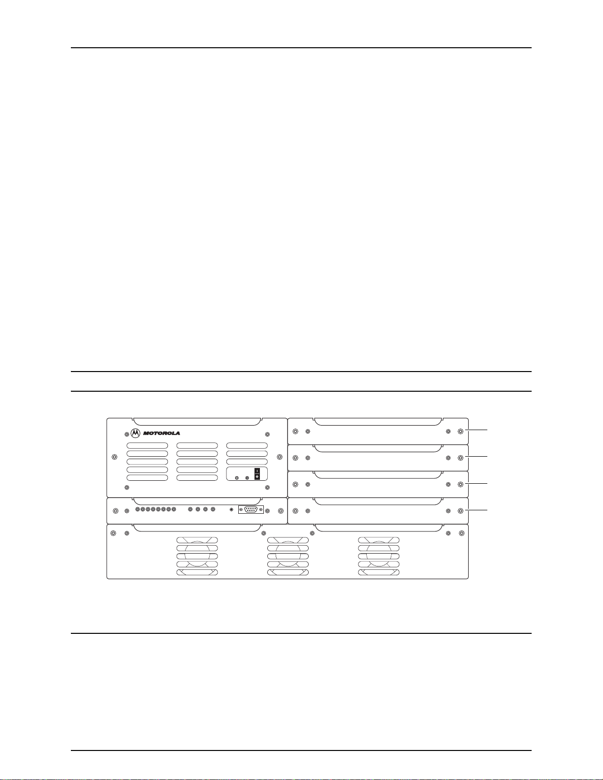
Figure 1-3 shows the front view of the BR.
Figure 1-3 QUAD Channel 900 MHz Base Radio (Typical)
QUAD CHANNEL POWER SUPPLY
TX4
TX4
TX4
PS
EX/CNTLPAREF
RX1
TX4
RX2
RX3
RX4
RESET
STATUS
900 QUAD CHANNEL EX/CNTL 900 QUAD CHANNEL RECEIVER
900 QUAD CHANNEL RECEIVER
900 QUAD CHANNEL RECEIVER
900 QUAD CHANNEL RECEIVER
900 QUAD CHANNEL POWER AMPLIFIER
EBTS282Q_900
120501JNM
RX4
RX3
RX2
RX1
Enhanced Base Transceiver System (EBTS)
16-June-06 68P80801E35-E 1-15
Page 20

Base Radio Volume 2
QUAD Channel 900 MHz Base Radio Overview
QUAD Channel 900
MHz Base Radio
Controls and
Indicators
QUAD Channel 900
MHz Base Radio
Performance
Specifications
Power Supply and EX / CNTL controls and indicators monitor BR status and
operating conditions, and also aid in fault isolation. The Power Supply and
EX / CNTL sections of this chapter discuss controls and indicators for both
modules.
The Power Supply has two front panel indicators. The EX / CNTL has twelve
front panel indicators. The Power Supply power switch applies power to the
BR. The EX / CNTL RESET switch resets the BR.
QUAD Channel 900 MHz Base Radio General Specifications
Table 1-9 lists general specifications for the BR.
Table 1-9 QUAD Channel 900 MHz BR General Specifications
Specification Value or Range
Dimensions:
Height
Width
Depth
Weight
5 EIA Rack Units (RU)
19" (482.6 mm)
16.75" (425 mm)
85 lbs. (38.6 kg)
Operating Temperature 32° to 104° F (0° to 40° C)
Storage Temperature -22° to 140° F (-30° to 60° C)
Rx Frequency Range:
900 MHz iDEN
Tx Frequency Range:
900 MHz iDEN 9
Tx – Rx Spacing:
900 MHz iDEN 39 MHz
Carrier Spacing 25 kHz
Carrier Capacity
Frequency Generation Synthesized
Digital Modulation QPSK, M-16QAM, and M-64QAM
Power Supply Inputs:
VDC -48 VDC (-41 to -60 VDC)
Diversity Branches Up to 3
*
901 - 902 MHz
40 - 941 MHz
1, 2, 3 or 4
Note * Multi-carrier operation must utilize adjacent, contiguous RF
carriers.
Enhanced Base Transceiver System (EBTS)
1-16 68P80801E35-E 16-June-06
Page 21

Volume 2 Base Radio
QUAD Channel 900 MHz Base Radio Overview
QUAD Channel 900 MHz Base Radio Transmit Specifications
Table 1-10 lists the BR transmit specifications.
Table 1-10 QUAD Channel 900 MHz BR Transmit Specifications
Specification Value or Range
Low average
output power per
Average Power Output:
(900 MHZ) Single Carrier 5.0W 52.0W
(900 MHz) Dual Carrier 2.5W 26.0W
(900 MHz) Triple Carrier 1.7W 16.1W
(900 MHz) QUAD Carrier 1.3W 10.5W
Transmit Bit Error Rate (BER) 0.01%
Occupied Bandwidth 18.5 kHz
Frequency Stability
RF Input Impedance 50 Ω (nom.)
FCC Designation (FCC Rule Part 24):
900 MHz QUAD BR ABZ89FC5798
*
carrier
1.5 ppm
High average
output power per
carrier
-P
Note * Transmit frequency stability locks to an external site reference,
which controls ultimate frequency stability to a level of 50 ppb.
QUAD Channel 900 MHz Base Radio Receive Specifications
Table 1-11 lis t s the receive specifications.
Table 1-11 QUAD Channel 900 MHz Receive Specifications
Specification Value or Range
Static Sensitivity †:
900 MHz BR -108 dBm (BER = 8%)
BER Floor (BER = 0.01%) ≥ -80 dBm
IF Frequencies
1st IF (All bands):
2nd IF:
Frequency Stability * 1.5 ppm
73.35 MHz (1st IF)
450 kHz (2nd IF)
Enhanced Base Transceiver System (EBTS)
16-June-06 68P80801E35-E 1-17
Page 22

Base Radio Volume 2
QUAD Channel 900 MHz Base Radio Overview
Table 1-11 QUAD Channel 900 MHz Receive Specifications
Specification Value or Range
RF Input Impedance 50 Ω (nom.)
FCC Designation (FCC Rule Part 15):
900 MHz BR ABZ89FR5799
Note † Measurement referenced from single receiver input port of BR.
Note * Stability without site reference connected to station. Receive
frequency stability locks to an external site reference, which controls ultimate
frequency stability to a level of 50 ppb.
QUAD Channel 900
MHz Base Radio
Theory of Operation
The QUAD Channel 900 MHz BR operates with other site controllers and
equipment and must be properly terminated. The following description
assumes such a configuration. Figure 1-10 show an overall block diagram of
the QUAD Channel 900 MHz BR.
Power is applied to the DC Power inputs located on the QUAD Channel 900
MHz BR backplane. The DC Power input is connected if -48 VDC or
batteries are used in the site.
Power is applied to the BR by setting the Power Supply power switch to the
ON position. Upon power-up, the QUAD Channel 900 MHz BR performs
self-diagnostic tests to ensure the integrity of the unit. These tests, which
include memory and Ethernet verification routines, primarily examine the EX
/ CNTL.
After completing self-diagnostic tests, the QUAD Channel 900 MHz BR
reports alarm conditions on any of its modules to the site controller via
Ethernet. Alarm conditions may also be verified locally. Local verification
involves using the service computer and the STA TUS port located on the front
of the QUAD Channel 900 MHz EX / CNTL.
The software resident in FLASH on the EX / CNTL registers the BR with the
site controller via Ethernet. After BR registration on initial power-up, the BR
software downloads via resident FLASH or Ethernet and executes from
RAM. The download includes operating parameters for the QUAD Channel
900 MHz BR. These parameters allow the QUAD Channel 900 MHz BR to
perform call processing functions.
Enhanced Base Transceiver System (EBTS)
1-18 68P80801E35-E 16-June-06
Page 23

Volume 2 Base Radio
QUAD Channel 900 MHz Base Radio Overview
After software downloads to the BR via Ethernet, FLASH memory stores the
software object. Upon future power-ups, the software object in FLASH loads
into RAM for execution.
The BR operates in a TDMA (Time Division Multiple Access) mode. This
mode, combined with voice compression techniques, increases channel
capacity by a ratio of as much as six to one. TDMA divides both the receive
and transmit signals of the BR into six individual time slots. Each receive slot
has a corresponding transmit slot. This pair of slots comprises a logical RF
channel.
The BR uses diversity reception for increased coverage area and improved
quality. The Receiver modules within the QUAD Channel 900 MHz BR
contain three receiver paths. Two-branch diversity sites use two Receiver
paths, and three-branch diversity sites use three Receiver paths.
All Receiver paths within a given Receiver module are programmed to the
same receive frequency. Signals from each receiver arrive at the EX / CNTL
module. This module performs a diversity combining algorithm on the
signals. The resultant signal undergoes an error-correction process. Then, via
Ethernet, the site controller acquires the signal, along with control information about signal destination.
Two separate FRUs comprise the transmit section of the QUAD Channel 900
MHz BR. These are the Exciter portion of the EX / CNTL and the Power
Amplifier (PA). The Exciter processes commands from the CNTL, assuring
transmission in the proper modulation format. Then the low-level signal
enters the PA. The PA amplifies this signal to the desired output power level.
The PA is a continuously keyed linear amplifier. A power control routine
monitors the output power of the BR. The routine adjusts the power as
necessary to maintain the proper output level.
Enhanced Base Transceiver System (EBTS)
16-June-06 68P80801E35-E 1-19
Page 24
Volume 2 Base Radio
Figure 1-10 800 and 900 MHZ QUAD Channel Base Radio Functional Block Diagram
ABACUS
RECEIVER
RX INTERFACE,
ADDRESS DECODE.
MEMORY, DIAGNOSTICS
ABACUS
RECEIVER
ABACUS
RECEIVER
Host SPI
EXCITER-BASE RADIO
CONTROLLER
STATUS
PORT
RS-232
ETHERNET
5 MHZ
EXTERNAL
REFERENCE
HOST
u’P
ETHERNET
INTERFACE
PLL/VCOs
BASE RADIO
CONTROLLER
DC POWER SUPPLY MODULE
EXTERNAL
DC INPUT
41 - 60 VDC
I
NPUT FILTER
START-UP
INVERTER
CIRCUITRY
IF FILTER
IC
IC
IC
AMP, AGC
IF FILTER
AMP, AGC
VCO SYNTH
SPLITTER
IF FILTER
AMP, AGC
Host SPI
ADDRESS DECODE,
MEMORY, ADC
133 KHZ
RX4 DATA
SDRAM
BUFFERS
IO LATCHES
EEPROM
16.8MHz
48MHz
Exciter
CLOCK
GENERATOR
MIXER
MIXER
MIXER
FLASH
267 KHZ
LPF, AMP,
FILTER
LPF, AMP,
FILTER
LPF, AMP,
FILTER
16.8MHz
LINEAR RF
AMPLIFIER
Main Converter
133 KHZ
RECEIVER 4
RECEIVE
DSP
TISIC
TRANSMIT
ODCT
RF IN
RECEIVER 4
PREAMPLIFIER
SPLITTER
/ BYPASS
RX3 DATA
1PPS & SLOT TIMING
DSP
I
Q
RF FEEDBACK
14.2 V
CONVERTER
Rx1&2
Rx3&4
RX SPI
TX RECLOCK
Tx_I Tx_Q
DAC
3.3 V
CONVERTER
RX2 DATA
RX1 DATA
RECEIVE
DSP
2.4MHz
VCOs/Synths
RF IN
FROM RFDS
(BRANCH 3)
QUAD RX IN DISTRIBUTION
SPI BUS
RF IN
FROM RFDS
(BRANCH 2)
SPI BUS
RF IN
FROM RFDS
(BRANCH 1)
+28 VDC
TO BACKPLANE
+14.2 VDC
TO BACKPLANE
+3.3 VDC
TO BACKPLANE
RECEIVER 3
RECEIVER 2
SPI BUS
SPI BUS
PREAMPLIFIER
SPLITTER
/ BYPAS S
PREAMPLIFIER
SPLITTER
/ BYPASS
RECEIVER 1
PREAMPLIFIER
SPLITTER
/ BYPASS
LPF, AMP,
FILTER
LPF, AMP,
FILTER
LPF, AMP,
FILTER
LPF, AMP,
FILTER
LPF, AMP,
FILTER
LPF, AMP,
FILTER
LPF, AMP,
FILTER
LPF, AMP,
FILTER
LPF, AMP,
FILTER
ADDRESS DECODE,
MEMORY, ADC
LINEAR
DRIVER
MIXER
MIXER
MIXER
MIXER
MIXER
MIXER
MIXER
MIXER
MIXER
SPLITTER
IF FILTER
AMP, AGC
IF FILTER
AMP, AGC
VCO SYNTH
SPLITTER
IF FILTER
AMP, AGC
IF FILTER
AMP, AGC
IF FILTER
AMP, AGC
VCO SYNTH
SPLITTER
IF FILTER
AMP, AGC
ABACUS
RECEIVER
IC
ABACUS
RECEIVER
IC
ABACUS
RECEIVER
IC
ABACUS
RECEIVER
IC
ABACUS
RECEIVER
IC
ABACUS
RECEIVER
IC
16.8MHz
IF FILTER
AMP, AGC
IF FILTER
AMP, AGC
VCO SYNTH
SPLITTER
IF FILTER
AMP, AGC
ABACUS
RECEIVER
IC
ABACUS
RECEIVER
IC
ABACUS
RECEIVER
IC
POWER AMPLIFIER MODULE
COMBINER
FINAL
LINEAR
AMPS
RX INTERFACE,
ADDRESS DECODE.
MEMORY, DIAGNOSTICS
RX INTERFACE,
ADDRESS DECODE.
MEMORY, DIAGNOSTICS
RX INTERFACE,
ADDRESS DECODE.
MEMORY, DIAGNOSTICS
RF OUT
TO RFDS
(TX ANTENNA)
Enhanced Base Transceiver System (EBTS)
16-June-06 68P80801E35-E 1-35
Page 25

Base Radio Controllers Volume 2
Overview
Overview 2
This chapter provides information on Base Radio Controllers (BRCs).
FRU Number to Kit
Number Cross
Reference
Base Radio Controller (BRC) Field Replaceable Units (FRUs) are available
for the iDEN EBTS. The FRU contains the BRC kit and required packaging.
Table 2-1 provides a cross reference between BRC FRU numbers and kit
numbers.
Table 2-1 FRU Number to Kit Number Cross Reference
FRU
Description
Single Channel 800 MHz Base Radio Controller TLN3334 CLN1469
Enhanced Base Radio Controller DLN6446 CLN1653
QUAD Channel 900 MHz Exciter/BR Controller DLN1203 CLF1792
QUAD Channel 800 MHz Exciter/BR Controller CLN1497 CLF1560
Number
Kit
Number
Enhanced Base Transceiver System (EBTS)
2-2 68P80801E35-E 16-June-06
Page 26
Base Radio Controllers Volume 2
900 MHz QUAD Channel Base Radio Controller
900 MHz QUAD Channel Base Radio Controller 2
900 MHz QUAD
Channel Base Radio
Controller Overview
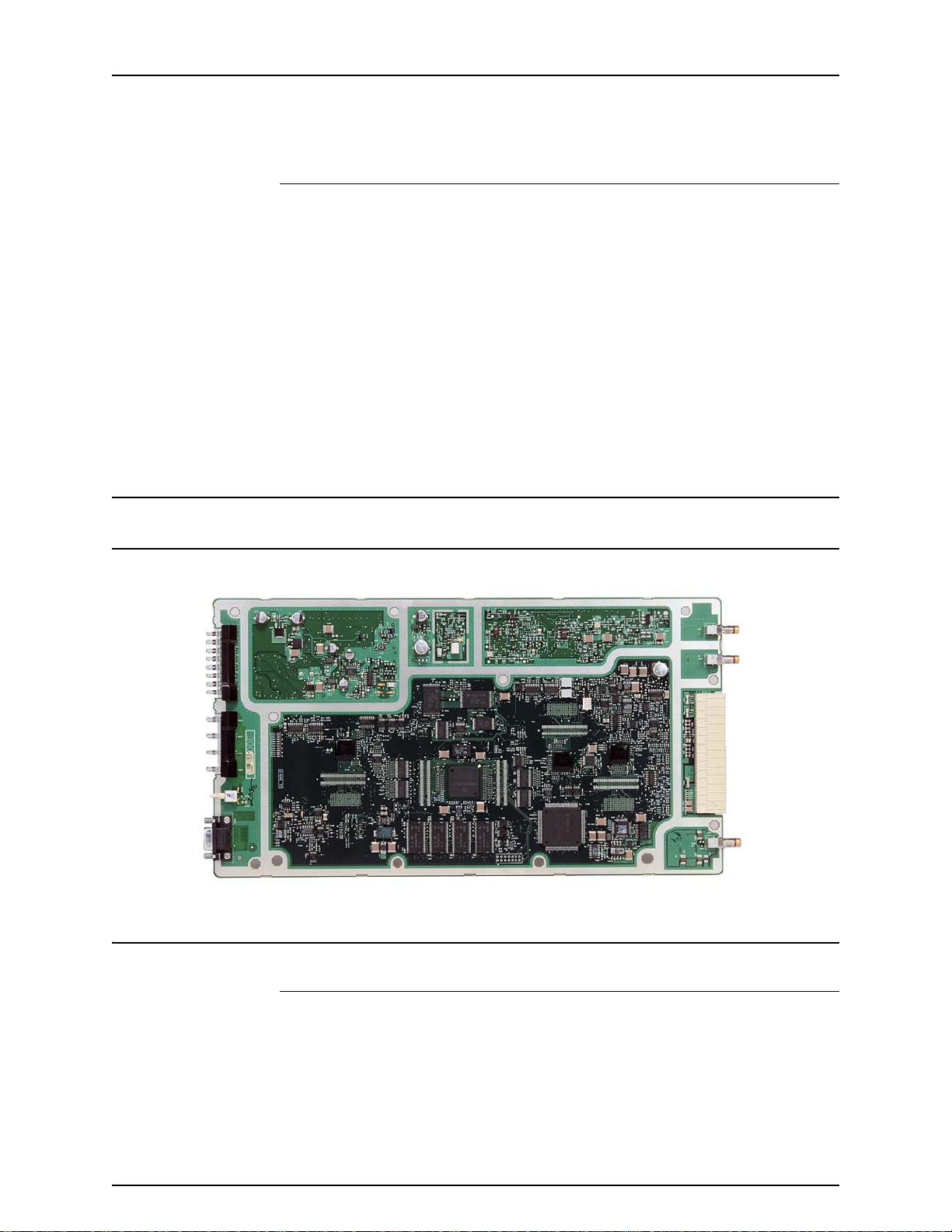
Figure 2-6 900 MHz QUAD Channel Base Radio Controller, version DLN1203 (with cover
removed)
The Base Radio Controller (BRC) provides signal processing and operational
control for Base Radio modules. The BRC module consists of a printed circuit
board, a slide-in housing, and associated hardware.
The BRC memory contains the operating software and codeplug. The
software defines BR operating parameters, such as output power and
operating frequency.
The BRC connects to the Base Radio backplane with one 168-pin FutureBus+
connector and one blindmate RF connector. Two Torx screws secure the BRC
in the Base Radio chassis.
Figure 2-6 shows a top view of the EX/CNTL (model CLF1560) with the
cover removed.
900 MHz QUAD
Channel Base Radio
Controller Controls
and Indicators
Enhanced Base Transceiver System (EBTS)
2-28 68P80801E35-E 16-June-06
The BRC monitors the functions of other Base Radio modules. The LEDs on
the front panel indicate the status of BRC-monitored modules. All LEDs on
the BRC front panel normally flash three times upon initial power-up. A
RESET switch allows a manual reset of the Base Radio. Figure 2-7 shows the
front panel of the BRC.
Page 27

Volume 2 Base Radio Controllers
900 MHz QUAD Channel Base Radio Controller
Figure 2-7 900 MHz QUAD Channel BR Controller (Front View)
PS
EX/CNTLPAREF
RX1
RX2
RX3
RX4
TX4
RESET
STATUS
QUAD CHANNEL EX/CNTL
EBTS316Q
013001JNM
TX4
TX4
TX4
Indicators
Table 2-12 lists and describes the BRC LEDs.
Table 2-12 900 MHz QUAD Channel BR Controller Indicators
Module
LED Color
PS Red Power Supply
EXBRC Red
PA Red
Monitored
Controller/
Exciter
Power
Amplifier
Condition Indications
Solid (on)
Flashing
(on)
Off Power Supply is operating normally (no alarms)
Solid (on)
Flashing
(on)
Off Controller/Exciter is operating normally (no alarms)
Solid (on)
Flashing
(on)
FRU failure indication - Power Supply has a major
alarm, and is out of service
Power Supply has a minor alarm, and may be operating
at reduced performance
FRU failure indication - Controller/Exciter has a major
alarm, and is out of service (Note: Upon power-up of the
BR, this LED indicates a failed mode until BR software
achieves a known state of operation.)
Controller/Exciter has a minor alarm, and may be
operating at reduced performance
FRU failure indication - PA has a major alarm, and is out
of service
PA has a minor alarm, and may be operating at reduced
performance
Off PA is operating normally (no alarms)
Enhanced Base Transceiver System (EBTS)
16-June-06 68P80801E35-E 2-29
Page 28

Base Radio Controllers Volume 2
900 MHz QUAD Channel Base Radio Controller
Table 2-12 900 MHz QUAD Channel BR Controller Indicators (continued)
Module
LED Color
Monitored
Condition Indications
Controller
REF Red
RX1
RX2
RX3
RX4
TX1 Green BR
TX2 Green BR
Red
Station
Reference
Receiver #1,
#2, #3, or #4
Solid (on)
Flashing
(on)
Off BRC is operating normally (no alarms)
Solid (on)
Flashing
(on)
Off
Solid (on) Station Transmit Carrier #1 is keyed
Flashing
(on)
Off Station is out of service, or power is removed
Solid (on) Station Transmit Carrier #2 is keyed
Flashing
(on)
FRU failure indication - Controller Station Reference
has a major alarm, and is out of service
BRC has a minor alarm, and may be operating in a
marginal region
FRU failure indication - Receiver (#1, #2, #3 or #4) has
a major alarm, and is out of service
Receiver (#1, #2, #3 or #4) has a minor alarm, and may
be operating at reduced performance
Receiver (#1, #2, #3 or #4) is operating normally (no
alarms)
Station Transmit Carrier #1 is not keyed
Station Transmit Carrier #2 is not keyed
TX3 Green BR
TX4 Green BR
Off Station is out of service, or power is removed
Solid (on) Station Transmit Carrier #3 is keyed
Flashing
(on)
Off Station is out of service, or power is removed
Solid (on) Station Transmit Carrier #4 is keyed
Flashing
(on)
Off
Station Transmit Carrier #3 is not keyed
Station Transmit Carrier #4 is not keyed
Station is out of service, or power is removed
Enhanced Base Transceiver System (EBTS)
2-30 68P80801E35-E 16-June-06
Page 29

Volume 2 Base Radio Controllers
900 MHz QUAD Channel Base Radio Controller
Controls
Table 2-13 lists the controls and descriptions.
Table 2-13 900 MHz QUAD Channel BR Controller Controls
Control Description
RESET Switch
STATUS connector
A push-button switch used to manually reset the
BR.
A 9-pin connector used for connection of a
service computer, providing a convenient
means for testing and configuring.
STATUS Connector
Table 2-14 the pin-outs for the STATUS connector.
Table 2-14 Pin-outs for the STATUS Connector
Pin-out Signal
1 not used
2TXD
3RXD
4 not used
5GND
6 not used
7 not used
8 not used
9 not used
Enhanced Base Transceiver System (EBTS)
16-June-06 68P80801E35-E 2-31
Page 30

Base Radio Controllers Volume 2
900 MHz QUAD Channel Base Radio Controller
900 MHz QUAD
Channel Base Radio
Controller Theory of
Operation
Table 2-15 briefly describes the BRC circuitry. Figure 2-14 is a functional
block diagram of the BRC.
Table 2-15 900 MHz QUAD Channel BR Controller Circuitry
Circuit Description
Host Microprocessor
Non-Volatile Memory
Volatile Memory
Ethernet Interface
RS-232 Interface
Digital Signal Processors
Contains integrated circuits that comprise the
central controller of the BRC and station
Consists of:
FLASH containing the station operating
software
EEPROM containing the station codeplug data
Contains SDRAM to store station software used
to execute commands.
Provides the BRC with a 10Base2 Ethernet
communication port to network both control and
compressed voice data
Provides the BRC with an RS-232 serial
interface
Performs high-speed modulation/demodulation
of compressed audio and signaling data
TISIC
TX Reclock
RX DSP SPI
Station Reference
Circuitry
Input Ports
Output Ports
Remote Station Shutdown
Contains integrated circuits that provide timing
reference signals for the station
Contains integrated circuits that provide highly
stable, reclocked transmit signals and
peripheral transmit logic
Contains integrated circuits that provide DSP
SPI capability and peripheral receive logic
Generates the 16.8 MHz and 48 MHz reference
signals used throughout the station
Contains 16 signal input ports that receive
miscellaneous inputs from the BR
Contains 40 signal output ports, providing a
path for sending miscellaneous control signals
to circuits throughout the BR
Provides software control to cycle power on the
BR
Enhanced Base Transceiver System (EBTS)
2-32 68P80801E35-E 16-June-06
Page 31

Volume 2 Base Radio Controllers
900 MHz QUAD Channel Base Radio Controller
Host Microprocessor
The host microprocessor is the main controller for the BR. The processor
operates at a 50-MHz clock speed. The processor controls Base Radio
operation according to station software in memory. S tation software resides in
FLASH memory. For normal operation, the system transfers this software to
non-volatile memory. An EEPROM contains the station codeplug.
Note At BR power-up, the EXBRC LED indicates a major alarm. This
indication continues until BR software achieves a predetermined state
of operation. Afterward, the software turns off the EXBRC LED.
Serial Communication Buses
The microprocessor provides a general-purpose SMC serial management
controller bus.
The SMC serial communications bus is an asynchronous RS-232 interface
with no hardware handshake capability. The BRC front panel includes a ninepin, D-type connector . This connector provides a port where service personnel
may connect a service computer. Service personnel can perform prog ramming
and maintenance tasks via Man-Machine Interface (MMI) commands. The
interface between the SMC port and the front- panel ST ATUS connector is via
EIA-232 Bus Receivers and Drivers.
Host Processor
The microprocessor incorporates 4k bytes of instruction cache and 4k bytes of
data cache that significantly enhance processor performance.
The microprocessor has a 32-line address bus. The processor uses this bus to
access non-volatile memory and SDRAM memory . V ia memory mapping, the
processor also uses this bus to control other BRC circuitry.
The microprocessor uses its Chip Select capability to decode addresses and
assert an output signal. The eight chip-select signals select non-volatile
memory, SDRAM memory, input ports, output ports, and DSPs.
The Host processor...
■ Provides serial communications between the Host Microprocessor and
other Base Radio modules.
■ Provides condition signals necessary to access SDRAM.
■ Accepts interrupt signals from BRC circuits (such as DSPs).
■ Organizes the interrupts, based on hardware-defined priority ranking.
■ The Host supports several internal interrupts from its Communications
Processor Module. These interrupts allow efficient use of peripheral
interfaces.
■ The Host supports 10 Mbps Ethernet/IEEE 802.3.
Enhanced Base Transceiver System (EBTS)
16-June-06 68P80801E35-E 2-33
Page 32

Base Radio Controllers Volume 2
900 MHz QUAD Channel Base Radio Controller
■ Provides a 32-line data bus transfers data to and from BRC SDRAM and
other BRC circuitry. Buffers on this data bus allow transfers to and from
non-volatile memory, general input and output ports and DSPs.
Non-Volatile Memory
Base Radio software resides in 2M x 32 bits of FLASH memory. The Host
Microprocessor addresses the FLASH memory with 20 of the host address
bus’ 32 lines. The host accesses FLASH data over the 32-line host data bus. A
host-operated chip-select line provides control signals for these transactions.
The FLASH contains the operating system and application code. The system
stores application code in FLASH for fast recovery from reset conditions.
Application code transfers from network or site controllers may occur in a
background mode. Background mode transfers allow the station to remain
operational during new code upgrades.
The data that determines the station personality resides in a 32K x eight bit
codeplug EEPROM. The microprocessor addresses the EEPROM with 15 of
the host address bus’ 32 lines. The host accesses EEPROM data with eight of
the data bus’ 32 lines. A host-operated chip-select line provides control
signals for these transactions.
During the manufacturing process, the factory programs the codeplug’s
default data. The BRC must download field programming data from network
and site controllers. This data includes operating frequencies and output
power level. The station permits adjustment of many station parameters, but
the station does not store these adjustments. Refer to the Software Commands
chapter for additional information.
Volatile Memory
Each BRC contains 8MB x 32 bits of SDRAM. The BRC downloads station
software code into SDRAM for station use. SDRAM also provides short-term
storage for data generated and required during normal operation. SDRAM is
volatile memory. A loss of power or system reset destroys SDRAM data.
The system performs read and write operations over the Host Address and
Data buses. These operations involve column and row select lines under
control of the Host processor’s DRAM controller. The Host address bus and
column row signals sequentially refresh SDRAM memory locations.
Ethernet Interface
The Host processor’s Communications Processor Module (CPM) provides the
Local Area Network (LAN) Controller for the Ethernet Interface. The LAN
function implements the CSMA/CD access method, which supports the IEEE
802.3 10Base2 standard.
Enhanced Base Transceiver System (EBTS)
2-34 68P80801E35-E 16-June-06
Page 33

Volume 2 Base Radio Controllers
900 MHz QUAD Channel Base Radio Controller
The LAN coprocessor supports all IEEE 802.3 Medium Access Control,
including the following:
■ framing
■ preamble generation
■ stripping
■ source address generation
■ destination address checking
The PCM LAN receives commands from the CPU.
The Ethernet Serial Interface works directly with the CPM LAN to perform
the following major functions:
■ 10 MHz transmit clock generation (obtained by dividing the 20 MHz signal
provided by on-board crystal)
■ Manchester encoding/decoding of frames
■ electrical interface to the Ethernet transceiver
An isolation transformer provides high-voltage protection. The transformer
also isolates the Ethernet Serial Interface (ESI) and the transceiver. The pulse
transformer has the following characteristics:
■ Minimum inductance of 75 µH
■ 2000 V isolation between primary and secondary windings
■ 1:1 Pulse Transformer
The Coaxial Transceiver Interface (CTI) is a coaxial cable line driver and
receiver for the Ethernet. CTI provides a 10Base2 connection via a coaxial
connector on the board. This device minimizes the number of external components necessary for Ethernet operations.
A DC/DC converter provides a constant voltage of -9 Vdc for the CTI from a
3.3 Vdc source.
The CTI performs the following functions:
■ Receives and transmits data to the Ethernet coaxial connection
■ Reports any collision that it detects on the coaxial connection
■ Disables the transmitter when packets are longer than the legal length
(Jabber Timer)
Enhanced Base Transceiver System (EBTS)
16-June-06 68P80801E35-E 2-35
Page 34

Base Radio Controllers Volume 2
900 MHz QUAD Channel Base Radio Controller
Digital Signal Processors
The BRC includes two Receive Digital Signal Processors (RXDSPs) and a
Transmit Digital Signal Processor (TXDSP). These DSPs and related circuitry
process compressed station transmit and receive audio or data. The related
circuitry includes the TDMA Infrastructure Support IC (TISIC) and the TISIC
Interface Circuitry. The DSPs only accept input and output signals in digitized
form.
The RXDSP inputs are digitized receiver signals. The TXDSP outputs are
digitized voice audio and data (modulation signals). These signals pass from
the DSP to the Exciter portion of the EXBRC. DSPs communicate with the
Microprocessor via an eight-bit, host data bus on the host processor side. For
all DSPs, interrupts drive communication with the host.
The RXDSPs operate from an external 16.8 MHz clock, provided by the local
station reference. The RXDSP internal operating clock signal is 150MHz,
produced by an internal Phase-Locked Loop (PLL).
The RXDSPs accept digitized signals from the receivers through Enhanced
Synchronous Serial Interface (ESSI) ports. Each of two ESSI ports on a
RXDSP supports a single carrier (single receiver) digital data input. The DSP
circuitry includes two RXDSPs. These allow processing of up to four carriers
(four receivers).
The RXDSP accesses its DSP program and signal-processing algorithms in
128k words of internal memory. The RXDSPs communicate with the host bus
over an 8-bit interface.
Each RXDSP provides serial communications to its respective receiver
module for receiver control via a Serial Peripheral Interface (SPI). The SPI is
a parallel-to-serial conversion circuit, connected to the RXDSP data bus. Each
RXDSP communicates to two receive modules through this interface.
Additionally , a serial control path conn ects the two RXDSPs and the TXDSP.
The Synchronous Communications Interface (SCI) port facilitates this serial
control path.
For initialization and control purposes, one RXDSP connects to the TISIC
device.
The TXDSP operates at an external clock speed of 16.8 MHz, provided by the
EXBRC local station reference. The TXDSP internal operating clock is
150MHz, produced by an internal Phase Lock Loop (PLL).
The TXDSP sends up to four carriers of digitized signal to the EX11 exciter.
The exciter converts the digital signal to analog. Also at the exciter, a highly
stable clock reclocks the digital data. Reclocking enhances transmit signal
integrity. Two framed and synchronized data streams result. One data stream
is I-data, and the other is the Q-data stream.
Enhanced Base Transceiver System (EBTS)
2-36 68P80801E35-E 16-June-06
Page 35

Volume 2 Base Radio Controllers
900 MHz QUAD Channel Base Radio Controller
The TXDSP contains its own, internal address and data memory. The TXDSP
can store 128k words of DSP program and data memory. An eight-bit
interface handles TXDSP-to-host bus communications.
TISIC
The TISIC controls internal DSP operations. This circuit provides the
following functions:
■ For initialization and control, interfaces with one RXDSP via the DSP
address and data buses.
■ Accepts a 16.8 MHz signal from Station Reference Circuitry.
■ Accepts a 5 MHz signal, modulated with one pulse per second (1 PPS) from
the site reference.
■ Demodulates the 1 PPS
■ Outputs a 1 PPS signal and a windowed version of this signal for network
timing alignment.
■ Outputs a 2.4 MHz reference signal used by the Exciter.
■ Generates 15 ms and 7.5 ms ticks. (These ticks synchronize to the 1 PPS
time mark. The system decodes the time mark from the site reference. Then
the system routes the reference to the TXDSP and RXDSPs.)
Station Reference Circuitry
The Station Reference Circuitry is a phase-locked loop (PLL). This PLL
consists of a high-stability, Voltage-Controlled, Crystal Oscillator (VCXO)
and a PLL IC. GPS output from the iSC connects to the 5 MHz/1 PPS BNC
connector on the BR backplane. Wiring at this connector routes signals to
EXBRC station reference circuitry.
The PLL compares the 5 MHz reference frequency to the 16.8 MHz VCXO
output. Then the PLL generates a DC correction voltage. The PLL applies this
correction voltage to the VCO through an analog gate. The analog gate closes
when three conditions coexist: (1) The 5 MHz tests stable. (2) The PLL IC is
programmed. (3) Two PLL oscillator and reference signal output alignments
occur.
When the gate enables, the control voltage from the PLL can adjust the highstability VCXO frequency. The adjustment can achieve a stability nearly
equivalent to that of the external, 5 MHz frequency reference.
The correction voltage from the PLL continuously adjusts the VXCO
frequency. The VXCO outputs a 16.8 MHz clock signal. The circuit applies
this clock signal to the receiver, 48 MHz reference and TISIC.
The receivers use the 16.8MHz as the clock input and synthesizer reference.
Enhanced Base Transceiver System (EBTS)
16-June-06 68P80801E35-E 2-37
Page 36

Base Radio Controllers Volume 2
900 MHz QUAD Channel Base Radio Controller
The 48 MHz EXBRC synthesizer uses the 16.8 MHz as its synthesizer
reference. The 48 MHz synthesizer output is the clock input for the TXDSP I
and Q data reclock circuitry.
The TISIC divides the 16.8 MHz signal by seven, and outputs a 2.4 MHz
signal. This output signal then becomes the 2.4 MHz reference for the Exciter.
Input Ports
One general-purpose input register provides for BRC and station circuit input
signals. The register has 16 input ports. The Host Data Bus conveys input
register data to the Host Microprocessor. Typical inputs include 16.8 and 48
MHz Station Reference Circuitry status outputs and reset status outputs.
Output Ports
Two general-purpose output registers distribute control signals from the Host
Microprocessor to the BRC and station circuitry. One register has 32 output
ports and the other register has 8 output ports. Control signal distribution
occurs over the backplane. The Host Data Bus drives the output ports’ latched
outputs. Typical control signals include front-panel LED signals and SPI
peripheral enable and address lines.
Remote Station Shutdown
The BRC contains power supply shutdown circuitry. This circuitry can send a
shutdown pulse to the Base Radio Power Supply. BRC software generates the
shutdown control pulse.
After receiving a shutdown pulse, the power supply turns off BR power. Shut
down power sources include 3.3, 28.6 and 14.2 Vdc sources throughout the
BR. Due to charges retained by BR storage elements, power supply voltages
may not reach zero. The shutdown only assures that the host processor enters
a power-on-reset state.
A remote site uses the shutdown function to perform a hard reset of all BR
modules.
Enhanced Base Transceiver System (EBTS)
2-38 68P80801E35-E 16-June-06
Page 37

Volume 2 Base Radio Controllers
Figure 2-14 800 and 900 MHz QUAD Channel Base Radio Controller Functional Block Diagram (Sheet 1 of 2)
LED
CONTROL
LINES
HOST
LATCH
P0 OUT
12
POWER
SUPPLY
EXCITER/
CONTROL
PA REF RX1 RX2 RX3 RX4 TX1 TX2 TX3 TX4
3.3V
P0_OUT
SHUTDOWN
CIRCUITRY
SHUTDOWN
(TO POWER
SUPPLY)
FRONT PANEL LEDS
5MHZ_1PPS
BASE RADIO
INPUT
5MHZ
1PPS
G
A
T
I
SYNTHESIZER
IC / CIRCUITRY
N
G
SPI
BUS
STATION REFERENCE CIRCUITRY
DISCONNECT/
CONNECT
CONTROL
PHASE
DETECTION/
FILTERING/
CONTROL
STEARING
LINE
HIGH
STA BILITY
VCXO
16.8 MHZ
REMOTE STATION
SHUTDOWN CIRCUITRY
SYNTHESIZER
16.8MHZ
IC / CIRCUITRY
SPI
BUS
TRANSMIT REFERENCE CIRCUITRY
PHASE
DETECTION/
FILTERING
STEARING
LINE
HIGH
STA BILITY
VCXO
48 MHZ
Enhanced Base Transceiver System (EBTS)
16-June-06 68P80801E35-E 2-55
Page 38

Base Radio Controllers Volume 2
Figure 2-15 800 and 900 MHz QUAD Channel Base Radio Controller Functional Block Diagram (Sheet 2 of 2)
RECEIVE
DIGITAL
SIGNAL
PROCESSOR
(RX DSP 2)
D[16:23]
D[16:23]
PA RA LLEL
TO SERIAL
CIRCUITRY
SPI BUS TO
RECEIVER 3 & 4
SPI BUS TO
RECEIVER 1 & 2
SERIAL MANAGEMENT CONTROLLER (SMC2)
2
EIA-232
BUS
RECEIVERS/
DRIVERS
2
STATUS PORT
(9 PIN D CONNECTOR
ON BRC FRONT PANEL)
RX1 SERIAL DATA
RX2 SERIAL DATA
DIFFERENTIAL
TO SINGLE END
DIFFERENTIAL
TO SINGLE END
HOST
MICRO-
PROCESSOR
SCC1
ETHERNET
SERIAL
INTERFACE
ETHERNET
SERIAL
8
CS2
CS3
INTERF AC E
SERIAL PERIPHERAL INTERFACE
HOST ADDRESS BUS
GPLA0, A[8,9,17,18,20:29],RAS,CAS,WE
SDRAM
4M x 16
SDRAM
4M x 16
D[0:31]
CS4
HOST BUFFERED ADDRESS BUS
CS0
CS1
MA[2:21]
FLASH
1M x 16
D[0:15]
D[16:31]
HOST DATA BUS
MD[0:15]
ETHERNET INTERF ACE
CLSN
RCV RX
ISOLATION
CD
TRANSFORMER
TRMT TX
3
BUFFER
DRAM MEMORY
SDRAM
D[0:15]
4M x 16
SDRAM
4M x 16
D[16:31]
MA[2:21]
FLASH
MD[0:15]
1M x 16
TRANSCEIVER
3
A[0:7]
D[0:31]
D[0:7]
MA[0:14]
SPI
BUS
A[10:31]
16
16
16
16
EXTENDED HOST
BUS BUFFERS
BUFFER
BUFFER
BUFFER
BUFFER
BUFFER
BUFFER
RX3 SERIAL DATA
10BASE2
COAX
SPI BUS
TO/FROM
STATION MODULES
16
16
16
16
RX4 SERIAL DATA
MA[21:0]
P0_IN
BUFFER
DSP_A[31:24]
MD[31:0]
DSP_D[31:24]
DIFFERENTIAL
TO SINGLE END
DIFFERENTIAL
TO SINGLE END
DIGITAL SIGNAL PROCESSING
CIRCUITRY
HOST-DSP BUFFERED ADDRESS BUS
HOST-DSP BUFFERED DATA BUS
HOST BUFFERED DATA BUS
MD[0:32]
P0_OUT
LATCH
32
RECEIVE
DIGITAL
SIGNAL
PROCESSOR
(RX DSP 1)
NETWORKED
SCI
TRANSMIT
DIGITAL
SIGNAL
PROCESSOR
(TX DSP)
DIGITAL SIGNAL PROCESSING
CIRCUITRY
D[0, 23]
D[0, 8:23]
A[0:5]
1 PPS TIMING, CONTROL/ SLOT TIMING/RESET
5MHZ
FRONT PANEL
RESET
1PPS
TRANSMIT
CLOCK AND
FRAME SYNCH
CIRCUITRY
I/Q DATA
DSP SPI
EXCITER
SPI
BUS
SPI
CONTROL
TISIC
48 MHZ
SINGLE END
TO DIFFERENTIAL
16.8MHZ
2.4 MHz
TO EXCITER
SERIAL DATA
TO EXCITER
SPI BUS
TO EXCITER
FLASH
1M x 16
MD[16:31]
EEPROM
32k x 8
MD[24:31]
8
MD[16,17,20-24,28-31]
EXPANDED STATUS INPUT
AND OUTPUT CONTROL CIRCUITRY
MD[24:31]
P1_OUT
LATCH
8
40
P0_OUT/P1_OUT
CONTROL BUS
TO
STATION MODULES
50 MHZ
CLOCK
P0_IN
STATUS BUS
STATION MODULES
FROM
FLASH
1M x 16
MD[16:31]
NON-VOLATILE MEMORY
Enhanced Base Transceiver System (EBTS)
2-56 68P80801E35-E 16-June-06
Page 39

Base Radio Exciter Volume 2
Overview
Overview 4
This chapter provides technical information for the Exciter (EX).
FRU Number to Kit
Number Cross
Reference
Exciter Field Replaceable Units (FRUs) are available for the iDEN EBTS.
The FRU contains the Exciter kit and required packaging. Table 4-1 provides
a cross reference between Exciter FRU numbers and kit numbers.
Table 4-1 FRU Number to Kit Number Cross Reference
FRU
Description
Single Channel Exciter (800 MHz) TLN3337 CLF1490
QUAD Channel 900 MHz Exciter/Base Radio
Controller)
QUAD Channel 800 MHz Exciter/Base Radio
Controller
LNODCT (Low Noise Offset Direct Conversion
Transmit) Exciter (800 MHz)
Number
CLN1497 CLF6452
CLN1497 CLF1560
TLN3337 CLF1789
Kit
Number
Enhanced Base Transceiver System (EBTS)
4-2 68P80801E35-E 16-June-06
Page 40

Base Radio Exciter Volume 2
QUAD Channel 900 MHz Exciter
QUAD Channel 900 MHz Exciter 4
QUAD Channel 900
MHz Exciter
Overview
Figure 4-3 900 MHz QUAD Channel Exciter (with cover removed)
The Exciter and the Power Amplifier (PA) provide the transmitter functions of
the QUAD Channel 900 MHz Base Radio. The Exciter module consists of a
printed circuit board, a slide in housing, and associated hardware. The BRC
shares the printed circuit board and housing.
The Exciter connects to the Base Radio backplane through a 168-pin
connector and two blindmate RF connectors. Controller and exciter circuitry
also interconnect on the Exciter/Controller module. T w o Torx screws on the
front of the Exciter secure it to the chassis.
An LED identifies the Exciter’s operational condition, as described in the
manual’s Controller section. The Base Radio section of the manual provides
specifications for transmitter circuitry. This information includes data on the
Exciter and PAs.
Figures 4-4 shows the Exciter with the cover removed.
Enhanced Base Transceiver System (EBTS)
4-12 68P80801E35-E 16-June-06
Page 41

Volume 2 Base Radio Exciter
QUAD Channel 900 MHz Exciter
900 MHz QUAD
Channel Exciter
Theory of Operation
Table 4-4 describes the basic circuitry of the Exciter. Figure 4-7 show the
QUAD Carrier Exciter’s functional block diagram.
Table 4-4 900 MHz Exciter Circuitry
Circuit Description
Up-converts baseband data to the transmit
frequency
Down-converts the PA feedback signal to
baseband
LNODCT IC
Memory & A/D Converter
Frequency Synthesizer
Circuitry
Uses a baseband Cartesian feedback loop
system, necessary to obtain linearity from the
transmitter and avoid splattering power into
adjacent channels
Performs training functions for proper
linearization of the transmitter
Serves as the main interface between the
synthesizer, Tranlin IC, A/D, and EEPROM on
the Exciter, and the BRC via the SPI bus
Consists of a phase-locked loop and VCO
Provides a LO signal to the LNODCT IC for the
second up-conversion and first downconversion of the feedback signal from the PA
1025 MHz VCO
(900 MHz BR)
90.3 MHz VCO
(900 MHz BR)
Regulator Circuitry
Linear RF amplifier Stages
Provides a LO signal to the LNODCT IC, for upconversion to the transmit frequency
Provides a LO signal to LNODCT IC, for the upconversion and for the down-conversion of the
feedback signal.
The mixed output becomes the LO signal for
Transmit signal up- and down- conversion
Provides a regulated voltage to various ICs and
RF devices located on the Exciter
Amplifies the RF signal from the Exciter IC to an
appropriate level for input to the PA
Enhanced Base Transceiver System (EBTS)
16-June-06 68P80801E35-E 4-13
Page 42

Base Radio Exciter Volume 2
QUAD Channel 900 MHz Exciter
Memory Circuitry
The memory circuitry is an EEPROM on the Controller portion of the Exciter/
Controller module. The Controller performs memory read and write operations over the parallel bus. The memory device stores the following data...
■ kit number
■ revision number
■ module specific scaling and correction factors
■ serial number
■ free form information (scratch pad)
A/D Converter Circuitry
Analog signals from various areas throughout the Exciter board enter the A/D
converter (A/DC). The A/DC converts these analog signals to digital form.
Upon request of the BRC, A/DC output signals enter the BRC via SPI lines.
The Controller periodically monitors all signals.
Some of the monitored signals include amplifier bias and synthesizer signals.
Low Noise Offset Direct Conversion Transmit (LNODCT) IC
Circuitry
The Low Noise IC is a main interface between the Exciter and BRC. The
BRC’s Digital Signal Processor (DSP) sends digitized signals (baseband data)
to the Exciter over the DSP data bus.
The differential data clock signal serves as a 2.4 MHz reference signal to the
Low Noise IC’s internal synthesizer. The Low Noise IC compares the
reference signal with the outputs of Voltage Controlled Oscillators (VCOs).
The Low Noise IC might sense that a VCO’s output is out of phase or offfrequency. If so, then the Low Noise IC sends correction pulses to the VCO.
The pulses adjust VCO output, thereby matching phase and frequency with
the reference.
The Low Noise IC up-converts baseband data from the BRC to the transmit
frequency. The Low Noise IC also down-converts the Transmit signal from
the Power Amplifier to baseband data for cartesian feedback linearization.
The BRC uses the Serial Peripheral Interface (SPI) bus to communicate with
the Low Noise IC. The SPI bus serves as a general purpose, bi-directional,
serial link between the BRC and other Base Radio modules, including the
Exciter. The SPI carries control and operational data signals to and from
Exciter circuits.
Enhanced Base Transceiver System (EBTS)
4-14 68P80801E35-E 16-June-06
Page 43

Volume 2 Base Radio Exciter
QUAD Channel 900 MHz Exciter
Synthesizer Circuitry
The synthesizer circuit consists of the Phase-Locked Loop (PLL) IC and
associated circuitry. This circuit’s controls the 1025 MHz VCO signal. An
internal phase detector generates a logic pulse. This pulse is proportional to
the phase or frequency difference between the reference frequency and loop
pulse signal.
The charge pump circuit generates a correction signal. The correction signal
moves up or down in response to phase detector output pulses. The correction
signal passes through the low-pass loop filter. The signal then enters the 1025
MHz Voltage Controlled Oscillator (VCO) circuit.
1025 MHz Voltage Controlled Oscillator (VCO)
For proper operation, the VCO requires a very low-noise, DC supply voltage.
An ultra low-pass filter prepares the necessary low-noise voltage and drives
the oscillator.
A portion of the oscillator output signal enters the synthesizer circuitry. The
circuitry uses this feedback signal to generate correction pulses.
The 1025MHz VCO output mixes with the 90.3 MHz VCO output. Th e result
is a Local Oscillator [LO) signal for the Low Noise IC. The LNODCT uses
this LO signal to up-convert the programmed transmit frequency. The Low
Noise IC also uses the LO signal to down-convert the PA feed back signal.
90.3 MHz Voltage Controlled Oscillator (VCO)
The synthesizer within the Low Noise IC sets the 90.3 MHz signal. The 90.3
MHz VCO provides a LO signal to the LNODCT IC. The Low Noise IC uses
this signal in up-converting and down-converting the feedback signal.
Regulator Circuitry
The voltage regulators generate three regulated voltages: +3 Vd c, +5 Vdc a nd
+11.7 Vdc. The regulators obtain input voltages from the +3.3 Vdc and +14.2
Vdc backplane voltages. The regulated voltages power various ICs and RF
devices in the Exciter.
Linear RF Amplifier Stages
The linear RF amplifiers boost the RF signal from the Low Noise IC. The RF
Amplifier generates an appropriate signal level to drive the PA.
Enhanced Base Transceiver System (EBTS)
16-June-06 68P80801E35-E 4-15
Page 44

Volume 2 Base Radio Exciter
Figure 4-7 800 and 900 MHz Exciter Board Functional Block Diagram
RF FEEDBACK
FROM PAMODULE
DIFFERENTIAL
DATA & CLOCK
FROM
BRC MODULE
ADDRESS BUS
FROM CONTROL
MODULE
SPI BUS
TO/FROM CONTROL
MODULE
LNODCT IC CIRCUITRY
TX DATA & CLOCK
90.3
VCO
CIRCUITRY
OSCILLATOR
BUFFER
AMP
ADDRESS DECODE, MEMORY, & A/D
CONVERTER CIRCUITRY
VARIOUS
SIGNALS
TO MONITOR
I
DAC
Q
MEMORY
A/D
CONVERTER
EXCITER IC CIRCUITRY
REGULATOR
CIRCUITRY
+14.2 V
FROM
BACKPLANE
+11.7 V
REGULATOR
LNODCT IC
LO
INJECTION
CIRCUITRY
+3.3 V
+3 V
REGULATOR
(U3702)
+5 V
REGULATOR
+3 V
SOURCE
+11.7 V
SOURCE
+5 V
SOURCE
970 MHZ
VCO CIRCUITRY
BUFFER
SYNTHESIZER
CIRCUITRY
2.4 MHZ
BUFFER
AMP
RIN
FIN
CHIP
SELECT
PHASE
LOCKED
LOOP
IC
OSCILLATOR
FEEDBACK
+10 V
FILTER
CONTROL VOLTAGE
VCO FEEDBACK
SPI BUS (CLOCK & DATA)
FROM BACKPLANE
CHARGE
PUMP
VCO
DC
LOW-PASS
LOOP
FILTER
LINEAR RF AMPLIFIER
CIRCUITRY
RF OUTPUT
TO PAMODULE
NOTE: Where two frequencies are given, frequency without parentheses applies to 800 MHz BR only and frequency with parentheses applies to 900 MHz BR only.
BPF
EBTS283Q
080601JNM
Enhanced Base Transceiver System (EBTS)
16-June-06 68P80801E35-E 4-23
Page 45

Power Amplifier Volume 2
Overview
Overview 5
This section provides technical information for the Power Amplifier (PA).
FRU Number to Kit
Number Cross
Reference
Power Amplifier (PA) Field Replaceable Units (FRUs) are available for the
iDEN EBTS. The FRU contains the PA kit and required packaging. Table 5- 1
provides a cross reference between PA FRU numbers and kit numbers.
Table 5-1 FRU Number to Kit Number Cross Reference
FRU
Description
40 W- 800 MHz Single Channel Base Radio PA TLF2020 CLF1772
70 W- 800 MHz Single Channel Base Radio PA TLN3335 CLF1771
52 W- 900 MHz QUAD Channel Base Radio PA DLN1202 CTF1082
52 W- 800 MHz QUAD Channel Base Radio PA CLF1499 CLF1400
QUAD+2 Channel Base Radio PA DLN6655 CLF1835
Number
Kit
Number
Enhanced Base Transceiver System (EBTS)
5-2 68P80801E35-E 16-June-06
Page 46

Volume 2 Power Amplifier
Power Amplifier Overview
Power Amplifier Overview 5
Note The power outputs discussed on this section for the 800 MHz QUAD
and 900 MHz QUAD Power Amplifiers are referenced to the single
carrier mode, operating at 52 W average power output from the Power
Amplifier’s output connector.
General Specifications of the transmitter circuitry, including the Exciter and PAs, are
provided in Base Radio Overview section. Figure 5-1 shows the 40W, 800
MHz PA. Figure 5-2 shows the 70W, 80 0 MHz PA. Figure 5-3 shows the 800
MHz QUAD PA (the 900 MHz QUAD PA is similar in appearance). Figure
5-4 shows the QUAD+2 PA.
40W-800 MHz, 70W-800 MHz, 800 MHz QUAD and 900 MHz
QUAD
The Power Amplifier (PA), with the Exciter, provides the transmitter
functions for the Base Radio. The PA accepts the low-level modulated RF
signal from the Exciter. The PA then amplifies the signal for transmission and
distributes the signal through the RF output connector.
The 800 MHz Base Radio can be equipped with either 40 Watt PA, TLF2020
(version CLF1771) or 70 Watt PA, TLN3335 (version CLF1772). The 40W
PA module consists of five hybrid modules, four pc boards, and a module
heatsink/housing assembly. The 70W PA module consists of eight hybrid
modules, four pc boards, and a module heatsink/housing assembly.
The PA connects to the chassis backplane through a 96-pin DIN connector
and three blindmate RF connectors. Two Torx screws located on the front of
the PA hold it in the chassis.
QUAD+2
The QUAD+2 Power Amplifier is a hot-swap capable, forced convection
cooled RF power amplifier. It accepts a low-level modulated RF signal from
the transceiver module, and amplifies it for transmission via the site transmit
antenna.
Enhanced Base Transceiver System (EBTS)
16-June-06 68P80801E35-E 5-3
Page 47

Power Amplifier Volume 2
Power Amplifier Overview
Figure 5-3 800/900 MHz QUAD PA
Figure 5-4 QUAD+2 PA
Enhanced Base Transceiver System (EBTS)
5-6 68P80801E35-E 16-June-06
Page 48

Volume 2 Power Amplifier
PA Theory of Operation
PA Theory of Operation 5
Table 5-2 describes the basic functions of the PA circuitry. Figures 5-5 and
5-6 show the functional block diagrams of 40W, 800 MHz and 70W , 800 MHz
P A, respectively. Figures 5-7 shows a functional block diagram of 800 QUAD
MHz. Figures 5-8 shows a functional block diagram of 900 MHz QUAD PA.
Figures 5-9 shows a functional block diagram of QUAD+2 PA.
Table 5-2 Power Amplifier Circuitry
Circuit Description
■ Serves as the main interface between the PA and the backplane
board
■ Accepts RF input from the Exciter via a blindmate RF connector
■ Routes the RF input via a 50 Ω stripline to the Linear Driver Module
RF amplifier
■ Routes the RF feedback from the RF Combiner/Peripheral Module to
the Exciter via a blindmate RF connector
DC/Metering Board
■ Provides digital alarm and metering information of the PA to the BRC
via the SPI bus
■ Routes DC power to the fans and PA
■ Contains the thermistor that senses the PA temperature (800 MHz
QUAD and 900 MHz QUAD)
■ Contains a Linear Driver Module and Linear Final Module Bias
Enable Circuit (900 MHz QUAD)
■ Contains a Voltage Variable Attenuator Circuit (900 MHz QUAD)
Linear Driver Module
(LDM)
Interconnect Board
■ Contains two Class AB stages with the final stage in a parallel
configuration (70W-800 MHz, 40W-800 MHz, 800 MHz QUAD)
■ Contains three cascaded Class AB stages with the first two stages
configured as distributed amplifiers and the final stage in parallel
configuration (900 MHz QUAD)
■ Amplifies the low level RF signal ~11mW average power from the
Exciter via the DC/Metering Board (70W-800 MHz, 800 MHz QUAD*,
900 MHz QUAD*)
■ Amplifies the low-level RF signal ~8 mW average power from the
Exciter via the DC/Metering Board (40W- 800 MHz)
■ Provides an output of:
~8 W (70W, 800MHz) average power
■ ~4 W (40W, 800 MHz) average power
■ ~6 W (800 MHz QUAD* and 900 MHz QUAD*) average power
■ Provides RF interconnection from the LDM to the RF Splitter board
■ Provides DC supply filtering
Enhanced Base Transceiver System (EBTS)
16-June-06 68P80801E35-E 5-7
Page 49

Power Amplifier Volume 2
PA Theory of Operation
Table 5-2 Power Amplifier Circuitry (continued)
Circuit Description
■ Interfaces with the DC/Metering Board to route DC power to the
LFMs
■ Interfaces with the DC/Metering Board to route PA Bias Enable to the
six Linear Final Modules (900 MHz Quad)
RF Splitter/DC board
Linear Final Module
(LFM)
■ Contains splitter circuits that split the RF output signal of the LDM to
the three Linear Final Modules (40W- 800 MHz)
■ Contains splitter circuits that split the RF output signal of the LDM to
the six Linear Final Modules (70W- 800 MHz, 800 MHz QUAD and
900 MHz QUAD)
■ Each module contains two Class AB amplifiers in parallel. Each
module amplifies one of three RF signals (~ 84 W average power)
from the LDM (via the Splitter/DC board). Three LFMs provide a sum
RF output of approximately 48 W average power, before losses.
(40W, 800MHz)
■ Each module contains two Class AB amplifiers in parallel. Each
module amplifies one of six RF signals (~ 8 W average power) from
the LDM (via the Splitter/DC board). Six LFMs provide a sum RF
output of approximately 97 W average power, before losses. (70W,
800MHz)
■ Each module contains two Class AB amplifiers in parallel. Each
module amplifies one of six RF signals (~6W average power) from
the LDM (via the splitter/DC Board). Six LFMs provide a sum RF
output of approximately 73W average power , before losses. (800
MHZ QUAD* and 900 MHz QUAD*)
RF Interconnect Board
(40W- 800 MHz PA only)
Combiner Board
(70W-800 MHz,
800 MHz QUAD, and
900 MHz QUAD only)
■ Contains three transmission lines that interconnect the LFMs to the
RF Combiner/Peripheral Module
■ Contains three separate Quadrature combiner circuits that
respectively combine the six RF outputs from the LFMs into three
signals. These three signals, in turn, are applied to the RF Combiner/
Peripheral Module.
Enhanced Base Transceiver System (EBTS)
5-8 68P80801E35-E 16-June-06
Page 50

Volume 2 Power Amplifier
PA Theory of Operation
Table 5-2 Power Amplifier Circuitry (continued)
Circuit Description
■ Contains a combiner circuit that combines the three RF signals from
the RF Interconnect Board (40W- 800 MHz PA) or the Combiner
Board (70W-800 MHz PA). It then routes the combined RF signal
through a single stage circulator and a Low Pass Filter. The final
output signal is routed to the blindmate RF connector (40W-800 MHz
and 70W-800 MHz PAs).
■ Contains a combiner circuit that combines the three RF signals from
the Combiner Board. It then routes the combined RF signal through
RF Combiner/Peripheral
Module
a dual stage circulator and a Low Pass Filter. The final output signal
is routed to the blindmate RF output connector. (800 MHz QUAD and
900 MHz QUAD PAs)
■ Contains an RF coupler that provides an RF feedback signal to the
Exciter via a blindmate RF connector on the DC/Metering Board.
Also contains a forward and reverse power detector for alarm and
power monitoring purposes.
■ Contains the thermistor that senses PA temperature and feeds the
signal back to the DC/Metering Board for processing (40W-800 MHz,
70W-800 MHz)
Fan Assembly
DC Core Board
(QUAD+2 only)
Driver Board
(QUAD+2 only)
Final Board
(QUAD+2 only)
Isolator Board
(QUAD+2 only)
Low Pass Filter Board
(QUAD+2 only)
■ Consists of three fans used to keep the PA within predetermined
operating temperatures
■ Provides Non-volatile memory (NVM) to store unique power amplifier
calibration information
■ Provides Gain and FB power control
■ Provides Diagnostic sensors
■ Provides Digital interface to the rest of the base radio
■ Provides Cooling measures control
■ Provides Status LEDs
■ Amplifies the output RF signal from the transceiver module (via the
core board) to an intermediate power level
■ Provides first two stages of RF amplification
■ Amplifies the output RF signal from the driver board (via the
distribution board).
■ Provides last two stages of RF amplification
■ Provides proper RF loading to the final module
■ Reduces harmonic power levels conducted through the PA RF
output connector to acceptable levels
Enhanced Base Transceiver System (EBTS)
16-June-06 68P80801E35-E 5-9
Page 51

Power Amplifier Volume 2
PA Theory of Operation
Table 5-2 Power Amplifier Circuitry (continued)
Circuit Description
Null Board
■ Provides +28Vdc to the Distribution Board
(QUAD+2 only)
Distribution Board
(QUAD+2 only)
■ Provides all signal routing from the Core and Null Boards to that of
the Final and Low Pass Filter boards
Note * The power outputs described in this section for the 800 QUAD and 900 QUAD PAs are
references to the single carrier mode operating at 52W average power out from the PA output connector.
DC/Metering Board Non-QUAD PA
The DC/Metering Board provides the interface between the PA and the Base
Radio backplane. The preamplified/modulated RF signal is input directly
from the Exciter via the Base Radio backplane.
The RF input signal is applied to the input of the Linear Driver Module
(LDM). The RF feedback signal is fed back to the Exciter, where it is
monitored for errors.
The primary function of the DC/Metering Boards is to monitor proper
operation of the PA. This information is forwarded to the Base Radio
Controller (BRC) via the SPI bus. The alarms diagnostic points monitored by
the BRC on the PA include the following:
■ Forward power
■ Reflected power
■ PA temperature sense
■ Fan Sensor
QUAD PA Only
The DC/Metering Board in the QUAD Radio serves the same function as it
does in other radios. However, its circuitry is modified for compatibility with
the QUAD Station. As a result, its logic circuitry is operated at 3.3 VDC.
In addition to the functions listed for non-QUAD versions above, the
following meter points are ported to the SPI bus:
■ A and B Currents
■ Thermistor (for PA temperature sensing circuit on the DC/Metering Board)
■ Voltage Variable Attenuator Circuit (900 MHz QUAD version)
■ PA Bias Enable Circuitry (900 MHz QUAD version)
Enhanced Base Transceiver System (EBTS)
5-10 68P80801E35-E 16-June-06
Page 52

Volume 2 Power Amplifier
PA Theory of Operation
Linear Driver Module 40W-800 MHz, 70W-800 MHZ and 800 MHZ QUAD PAs
The Linear Driver Module (LDM) amplifies the low-level RF signal from the
Exciter. The LDM consists of a two-stage cascaded Class AB amplifier, with
the final stage in a parallel configuration.
See Table 5-2 for the approximate input and output levels of the various
LDMs. The LDM output is fed to the RF Splitter/DC Distribution Board via
an Interconnect Board.
900 QUAD PA
The Linear Driver Module (LDM) amplifies the low-level RF signal from the
Exciter. The LDM consists of a three stage, cascaded, Class AB amplifier,
with the final stage in a parallel configuration.
See Table 5-2 for the approximate input and output power of the 900 MHz
QUAD LDM.
The LDM Output is fed to the RF Splitter/DC Distribution Board via the
Interconnect Board.
Interconnect Board The output of the LDM is applied to the Interconnect Board, which provides
an RF connection to the RF Splitter/DC Distribution Board. As a separate
function, area on the Interconnect Board serves as a convenient mounting
location for electrolytic capacitors used for filtering the +28 VDC supply.
RF Splitter/DC
Distribution Board
The RF Splitter portion of this board accepts the amplified signal from the
LDM (via the Interconnect Board). The primary function of this circuit is to
split the RF signal into drive signals for the LFMs.
In the 40W-800 MHz PA, this circuit splits the drive signal into three separate
paths to be applied to the three LFMs, where the signals will be amplified
further. In the 70W-800 MHz, 800 MHz QUAD and 900 MHZ QUAD PAs,
this circuit splits the drive signal into six separate paths to be applied to the six
LFMs, where the signals will be amplified further.
The DC Distribution portion of this board interfaces directly with the DC/
Metering Board to route DC power to the LFMs and provide PA Bias Enable
(900 MHz QUAD only)
Enhanced Base Transceiver System (EBTS)
16-June-06 68P80801E35-E 5-11
Page 53

Power Amplifier Volume 2
PA Theory of Operation
Linear Final Modules The RF Splitter output signals are applied directly into the LFMs for final
amplification. Each LFM contains a coupler that splits the LFM input signal
and feeds the parallel Class AB amplifiers that amplify the RF signals.
In the 40W PA, the amplified signals are then combined on the LFM and sent
directly to the RF Interconnect Board. In the 70W PA, the amplified signals
are then combined on the LFM and sent directly to the Combiner Board.
See Table 5-2 for the approximate total summed output powers of the various
LFMs, before output losses.
RF Interconnect
40W- 800 MHz PA Only
Board
The RF Interconnect Board consists of transmission line paths which route the
three output signals from the LFMs to the three inputs of the RF Combiner/
Peripheral Module.
Combiner Board The Combiner Board combines pairs of signals into single signals, thereby
combining the six signals from the LDMs into three signals. The resulting
three signals are applied to the RF Combiner/Peripheral Module.
RF Combiner/
40- 800 MHz, 70W- 800 MHz PAs
Peripheral Module
This module consists of two portions: an RF combiner and a peripheral
module. The RF Combiner portion of the module combines the three RF
signals from the RF Interconnect Board (40W- 800 MHz PA) or the Combiner
Board (70W- 800 MHz PA) into a single signal using a Wilkinson coupler
arrangement.
Following the combiner circuit, the single combined RF signal is then passed
through a directional coupler which derives a signal sample of the LFM RF
power output. Via the coupler, a sample of the RF output signal is fed to the
Exciter, via the DC/Me t eri ng Boa r d, as a feedback signal. Following the
coupler, the power output signal is passed through a single stage circulator,
which protects the PA in the event of high reflected power.
The peripheral portion of the module provides a power monitor circuit that
monitors the forward and reflected power of the output signal. This circuit
furnishes the A/D converter on the DC/Metering Board with input signals
representative of the forward and reflected power levels.
Enhanced Base Transceiver System (EBTS)
5-12 68P80801E35-E 16-June-06
Page 54

Volume 2 Power Amplifier
PA Theory of Operation
For forward power, a signal representative of the measur ed value is sent to the
BRC via the SPI bus. The BRC determines if this level is within tolerance of
the programmed forward power level. If the level is not within parameters,
the BRC will issue a warning to the site controller which, in turn, will shut
down the Exciter if required.
Reflected power is monitored in the same manner. The BRC uses the
reflected power to calculate the voltage standing wave ratio (VSWR). If the
VSWR is determined to be excessive, the forward power is rolled back. If it is
extremely excessive, the BRC issues a shut-down command to the Exciter.
A thermistor is located on the RF Combiner/Peripheral module to monitor the
operating temperature of the PA. The thermistor signal indicating excessive
temperature is applied to the A/D converter and then sent to the BRC. The
BRC issues a cut-back command to the Exciter module if the monitored
temperature is greater than 185° F (85° C).
800 MHz QUAD and 900 MHz QUAD
This module consists of two parts: an RF combiner and a Peripheral module.
The RF combiner combines three RF signals from the Combiner Board into a
single signal using a Wilkinson coupler arrangement. Following the combiner
circuit, the single combined RF signal is then passed through a directional
coupler, which derives a signal sample of the LFM RF power output. Via the
coupler, a sample of the RF output signal is fed to the Exciter, via the DC/
Metering Board, as a feedback signal. Following the coupler , the power output
signal is passed through a dual stage circulator, which protects the PA in the
event of high reflected power.
The Peripheral module provides a power monitor circuit that monitors the
forward and reflected power of the output signal. This circuit furnishes the A/
D converter on the DC/Metering Board with input signals, representative of
the forward and reflected power levels.
For forward power, a signal representative of the measur ed value is sent to the
BRC via the SPI bus. The BRC determines if this level is within tolerance of
the programmed forward power level. If the level is not within tolerance, the
BRC will issue a warning to the site controller, which, in turn, will shut down
the Exciter, if required.
Reflected power is monitored in the same manner. The BRC uses the reflected
power to calculate the voltage standing wave ratio (VSWR). If the VSWR is
calculated as excessive, forward power is rolled back. If the VSWR calculation is exceedingly out of tolerance, the BRC issues a shut-down command
to the Exciter.
The Thermistor that monitors the operating temperature of the 800 MHZ
QUAD and 900 MHz QUAD PAs is located on the DC/Metering Board
Enhanced Base Transceiver System (EBTS)
16-June-06 68P80801E35-E 5-13
Page 55

Power Amplifier Volume 2
PA Theory of Operation
Fan Module The PA contains a fan assembly to maintain normal operating temperature
through the use of a cool air intake. The fan assembly consists of three
individual fans in which airflow is directed across the PA heatsink.
The current draw of the fans is monitored by the DC/Metering Board. A
voltage representative of the current draw is monitored by the BRC. The BRC
flags the iSC if an alarm is triggered. The PA LED on the front panel of the
BRC also lights, however the PA does not shut down due to a fan failure
alone.
DC Core Board
(QUAD+2)
Driver Board
(QUAD+2)
Final Board
(QUAD+2)
The Core Board communicates with the other base radio modules as well as
internal P A modules. It utilizes non-volatile memory (NVM) via an EEPROM
to store unique PA calibration information.
The Driver Amplifier Board provides the first two stages of RF amplification
within the PA. It accepts the output RF signal from the transceiver module
(via the core board) and amplifies it to an intermediate power level. The
Driver Amplifier Board also provides:
■ Gain compensation over temperature.
■ On-board DC regulation.
■ Transmitter standby functionality
The Final Amplifier Board provides the last two stages of RF amplification,
including the second RF gain stage (parallel stage). QUAD+2 utilizes two
Final Amplifier Boards.:
■ RF power splitting (4–way)
■ RF power combining (4–way)
■ Diagnostics
■ Transmitter standby functionality
Isolator Board
(QUAD+2)
The Isolator provides proper RF loading to the final module output regardless
of the load presented to the output of the PA itself. The Isolator contains a
load resistor to dissipate any reflected power caused by load mismatches at
the output of the PA.
Enhanced Base Transceiver System (EBTS)
5-14 68P80801E35-E 16-June-06
Page 56

Volume 2 Power Amplifier
PA Theory of Operation
Low Pass Filter
(LPF) Board
(QUAD+2)
Null Board
(QUAD+2)
Distribution Board
(QUAD+2)
The LPF Board reduces harmonic power levels conducted through the PA RF
output connector to acceptable levels. The LPF Board has forward and
feedback RF power detectors to monitor forward and reflected output power
from the PA, in reference to its output connector. It has a single stage isolator
that provides > 20dB isolation with < 0.35dB insertion loss. It also p rovi des a
low pass filter with < 0.54dB of in-band insertion loss.
The Null Board provides the +28Vdc supply routing from the Core board to
the Distribution board (which routes it to the Final board). It also provides the
necessary bulk capacitance that is warranted by the Final board.
The Distribution Board provides for all signal routing from the Core and the
Null boards to the Final and LPF boards:
■ RF signal from the driver module is split and provided as the input to each
of the two final modules.
■ RF output from both of the final modules is combined to a single path and
provided as the input to the isolator.
■ RF power is coupled off the combined port and fed back to the XCVR
■ DC Power routing from the NULL board to the Final board
■ Forward and reverse DC signaling from the LPF board
Enhanced Base Transceiver System (EBTS)
16-June-06 68P80801E35-E 5-15
Page 57

Power Amplifier Volume 2
Figure 5-8 900 MHz QUAD Power Amplifier Functional Block Diagram
RF INPUT
SPI BUS
TO/FROM BRC
ADDRESS BUS
FROM BRC
ADDRESS DECODE, MEMORY,
& A/D CONVERTER CIRCUITRY
EEPOT
C_E
INC
V_D
CLK/DATA
MEMORY
CHIP SELECT
DECODE
CIRCUITRY
BOARD SELECT
DECODE
CIRCUITRY
VVA
PA_ENABLE (PA_E)
CHIP SELECT
CHIP
SELECT
A/D
CONVERTER
LINEAR DRIVER MODULE
STAGE 1
CLASS AB
DISTRIBUTED
FAN SENSE
PATEMP SENSE
FWD PWR
REF PWR
STAGE 2
CLASS AB
DISTRIBUTED
PA_E
STAGE 2
CLASS AB
FAN ASSEMBLY
INTERCONNECT
BOARD
FILTER
+28 VDC
DC
PA_E PA_E
RF SPLITTER/DC
DISTRIBUTION BOARD
50 OHM
LOAD
LOAD
50 OHM
LOAD
LOAD
50 OHM
50 OHM
PA_E
PA_E
PA_E
PA_E
LINEAR FINAL
MODULES
PA_E
PA_E
PA_E
PA_E
PA_E
COMBINER
BOARD
50 OHM
LOAD
50 OHM
LOAD
50 OHM
LOAD
RF OUT
TO ANTENNA
RF FEEDBACK
TO EXCITER
MODULE
Enhanced Base Transceiver System (EBTS)
LOW-PASS
FILTER
50 OHM
LOAD
CIRCULATOR
50 OHM
LOAD
CIRCULATOR
TEMPERATURE
SENSOR
RF COMBINER/
PERIPHERAL MODULE
50 OHM
LOAD
50 OHM
LOAD
LOAD
50 OHM
PA_E
STAGE 3
CLASS AB
PA_E
EBTS417_900
121701JNM
5-20 68P80801E35-E 16-June-06
Page 58

Power Supply Volume 2
Overview
Overview 6
This section provides technical information for the DC Power Supply (PS).
FRU Number to Kit
Number Cross
Reference
DC Power Supply Field Replaceable Units (FRUs) are available for the iDEN
EBTS. The FRU contains the Power Supply kit and required packaging. Table
6-1 provides a cross reference between Exciter FRU numbers and kit
numbers.
Table 6-1 FRU Number to Kit Number Cross Reference
FRU
Description
Single Channel DC Power Supply TLN3338 CPN1027
QUAD Channel DC Power Supply CLN1498 CLN1461
QUAD+2 Channel DC Power Supply DLN6568 CPN1081
Number
Kit
Number
Enhanced Base Transceiver System (EBTS)
6-2 68P80801E35-E 16-June-06
Page 59

Power Supply Volume 2
DC Power Supply for QUAD Channel Base Radios
DC Power Supply for QUAD Channel Base Radios 6
QUAD Channel DC
Power Supply
Overview
The QUAD Channel DC Power Supply provides DC operating voltages to
QUAD Channel Base Radio FRUs. The power supply accepts input voltage
sources from 41VDC to 60VDC. Input sources may be either positively or
negatively grounded.
On initial startup, the supply requires a nominal 43 VDC. If the voltage drops
below 41 VDC, the QUAD Channel DC Power Supply enters quiescent mode.
In quiescent mode, the power supply emits no power.
The QUAD Channel DC Power Supply is designed for sites with an available
DC voltage source. Output voltages from the DC Power Supply are 28.6
VDC, 14.2 VDC and 3.3 VDC, with reference to output ground. The supply is
rated for 575 Watts of continuous output, with up to 113° F (45° C) inlet air.
At 140° F (60° C), the 28.6 VDC output reduces to 80% of maximum.
The QUAD Channel DC Power Supply consists of the Power Supply and
front panel hardware. The QUAD Channel DC Power Supply connects to the
chassis backplane through an edgecard connector. Two Torx screws on the
front panel secure the QUAD Channel DC power supply to the chassis.
Figure 6-2 shows the QUAD Channel Power Supply with the cover removed.
Figure 6-2 Quad Carrier Power Supply
Enhanced Base Transceiver System (EBTS)
6-6 68P80801E35-E 16-June-06
Page 60

Volume 2 Power Supply
DC Power Supply for QUAD Channel Base Radios
QUAD Channel DC
Power Supply
Controls and
Indicators
QUAD Channel DC
Power Supply
Performance
Specifications
Table 6-5 summarizes LED indications on the QUAD Channel DC Power
Supply during normal operation. The ON/OFF switch behind the front panel
turns DC power supply on and off.
Table 6-5 DC Power Supply Indicators
LED Condition Indications
Solid (on)
Green
Off
Solid (on)
Red
Off
Power Supply is on, and operating under normal
conditions with no alarms
Power Supply is turned off or required power is
not available
Power Supply fault or load fault on any output, or
input voltage is out of range
Power Supply is operating normally, with no
alarms
Table 6-6 lists the specifications for the QUAD Channel DC Power Supply.
Table 6-6 DC Power Supply Specifications
Description Value or Range
Operating Temperature
Input Voltage 41 to 60 VDC
Input Polarity Positive (+) ground system
Startup Voltage 43 VDC (minimum)
Input Current 18.0 A (maximum) @ 41 VDC
Steady State Output Voltages
Total Output Power Rating
0° to +40° C (no derating)
+41° to +60° C (derating)
28.6 VDC +
14.2 VDC +
3.3 VDC +
575 W (no derating)
485 W (derating)
5%
5%
5%
Enhanced Base Transceiver System (EBTS)
16-June-06 68P80801E35-E 6-7
Page 61

Power Supply Volume 2
DC Power Supply for QUAD Channel Base Radios
Table 6-6 DC Power Supply Specifications (continued)
Description Value or Range
All outputs 150mV p-p (measured with
20 MHz BW oscilloscope at 25°C)
High Frequency individual harmonic
voltage limits (10kHz to 100MHz) are:
Output Ripple
Short Circuit Current 0.5 A average (maximum)
28.6 VDC 1.5 mV p-p
14.2 VDC 3.0 mV p-p
3.3 VDC 5.0 mV p-p
QUAD Channel DC
Power Supply
Theory of Operation
Table 6-7 briefly describes the basic DC Power Supply circuitry. Figure 6-6
shows the functional block diagrams for the DC Power Supply.
Table 6-7 DC Power Supply Circuitry
Circuit Description
Routes input current from the DC power input cable
Input Circuit
Startup Inverter
Circuitry
Main Inverter Circuitry
Temperature
Protection
+14.2 VDC
Secondary Converter
Circuitry
through the high current printed circuit edge
connector, EMI filter, panel mounted combination
circuit breaker, and on/off switch
Provides VDC for power supply circuitry during initial
power-up
Consists of a switching-type power supply to
generate the +28.6 VDC supply voltage
The Power Supply contains a built-in cooling fan that
runs whenever the supply is powered on. The supply
shuts down if the temperature exceeds a preset
threshold
Consists of a switching-type power supply to
generate the +14.2 VDC supply voltage
+3.3 VDC Secondary
Converter Circuitry
Clock Generator
Circuitry
Address Decode,
Memory, & A/D
Converter
Consists of a switching-type power supply to
generate the +3.3 VDC supply voltage
Generates the 267 kHz and 133 kHz clock signals
used by the pulse width modulators in the four
inverter circuits
Serves as the main interface between A/D on the
Power Supply and the BRC via the SPI bus
Enhanced Base Transceiver System (EBTS)
6-8 68P80801E35-E 16-June-06
Page 62

Volume 2 Power Supply
Figure 6-6 QUAD DC Power Supply Functional Block Diagram (Sheet 1 of 2)
EXTERNAL
DC INPUT
41-60 VDC
INPUT FILTER BOARD
VCC
PULSE
WIDTH
MODULATOR
FILTER
CIRCUITRY
TRANSISTOR
A
FRONT PANEL
ON / OFF
SWITCH
STARTUP INVERTER CIRCUITRY
STARTUP ISOLATION
VCC
TRANSFORMER
SWITCH
MAIN INVERTER CIRCUITRY
SOFTSTART
CIRCUITRY
SHUTDOWN
+12V STARTUP BIAS
PULSE
WIDTH
MODULATOR
267 KHZ
+12V STARTUP BIAS
VCC
VCC
PULSE
WIDTH
MODULATOR
TRANSISTOR
DRIVERS
VCC
133 KHZ
133 KHZ
VCC
FET
DRIVER
+28 V BULK
POWER FET
SWITCHES
POWER FET
SWITCH
MAIN ISOLATION
TRANSFORMER
133 KHZ
133 KHZ
+ 14.2V OVERCURRENT
DETECT
FILTER
CIRCUITRY
REF
REF
CURRENT
DETECT
SURGE CURRENT
DELAY
FILTERING
CIRCUITRY
REF
REF
+28 V BULK TO
+28.6 V OVERVOLTAGE
DETECT
REF
OVERCURRENT
DETECT
+14.2 V INVERTER CIRCUITRY
+14.2V
FET
OVERVOLTAGE
DETECT
DIAGNOSTICS
CIRCUITRY
CROWBAR
CIRCUIT
MOD FAIL
+28.6 VDC
+14.2V
P/O
BACKPLANE
CONNECTOR
3
4
14
15
P/O
BACKPLANE
CONNECTOR
16
17
22
23
A
B
+28.6 VDC
STATION
MODULES
BACKPLANE
A
+14.2V DC
STATION
MODULES
BACKPLANE
TO
VIA
TO
VIA
BULK DETECT
133 KHZ
CLOCK GENERATOR CIRCUITRY
CLOCK
GENERATOR
CIRCUITRY
267 KHZ
267 KHZ
÷ 2
133 KHZ
TO
DIAGNOSTICS
CIRCUITRY
267 KHZ
133 KHZ
VCC
PULSE
WIDTH
MODULATOR
VCC
FET
DRIVER
+ 28V BULK
POWER FET
SWITCH
133 KHZ
+ 5V OVERCURRENT
DETECT
FILTER
CIRCUITRY
REF
REF
SURGE CURRENT
DELAY
REF
+5.1 V INVERTER CIRCUITRY
FET
OVERVOLTAGE
DETECT
CROWBAR
CIRCUIT
CONNECTOR
+5.1 V
P/O
BACKPLANE
24
25
30
31
A
+5.1 V DC
TO
STATION
MODULES
VIA
BACKPLANE
EBTS323
011497JNM
Enhanced Base Transceiver System (EBTS)
16-June-06 68P80801E35-E 6-17
Page 63

Power Supply Volume 2
Figure 6-7 QUAD DC Power Supply Functional Block Diagram (Sheet 2 of 2)
B
BULK DETECT
FROM STARTUP
INVERTER
CIRCUITRY
DIAGNOSTICS CIRCUITRY
REF
REF
REF
HEATSINK STATUS
DETECT
HI-TEMP
DETECT
REF
REF
MODULE
FAIL
(RED)
MOD FAIL
INPUT FAIL
HEATSINK DIAG
REF
INPUT GOOD
(GREEN)
A
J300
COOLING
FAN
+5.1 V
A/D
CONVERTER
SPI BUS
3
SPI BUS
TO/FROM
STATION CONTROL
MODULE
FROM
STATION
CONTROL
BOARD
ADDRESS DECODE CIRCUITRY
P/O ADDRESS BUS
9
T°
ADDRESS
DECODE
CIRCUITRY
THERMISTOR
MOUNTED ON
HEATSINK
ENABLE
FROM
DETECT
CIRCUITRY
+14.2V DIAG
+5.1 V DIAG
+28.6 V DIAG
ENABLE
EBTS324
012097JNM
Enhanced Base Transceiver System (EBTS)
6-18 68P80801E35-E 16-June-06
Page 64

Troubleshooting Volume 2
Overview
Overview
This chapter is a guide for isolating Base Radio failures to the FRU level.
There are three sections- one each for Legacy Single Channel Base Radios,
Generation 2 Single Channel Base Radios, QUAD Channel Base Radios and
QUAD+2 Channel Base Radios. Each section contains procedures for:
n Troubleshooting
n Verification/Station Operation
The maintenance philosophy for any Base Radio is to repair by replacing
defective FRUs with new FRUs. This method limits down-time.
Two troubleshooting procedures are included. Each procedure is designed to
quickly identify faulty FRUs.
Ship defective FRUs to a Motorola repair depot for repair.
Note Any product damage resulting from improperly packaged equipment
will not be covered under the standard Motorola warranty agreement.
Enhanced Base Transceiver System (EBTS)
8-2 6880801E35-E 22-Mar-06
Page 65

Volume 2 Troubleshooting
Troubleshooting Preliminaries
Troubleshooting Preliminaries
Recommended Test
Equipment
Table 8-1 lists recommended test equipment necessary for performing Base
Radio troubleshooting/verification procedures.
Table 8-1 Recommended Test Equipment
Equipment Model/Type Manufacturer Description
Service Computer † 80286 or better
Application Code n/a Motorola
Communication
Software
RS-232 Cable n/a Locally Procured
RF Attenuator,
250W, 10dB
RF Power Meter††
ProComm Plus
HyperTerminal
01-80301E72
58-45-33
HP438A
E4418
IBM, IBM compatible, or
Macintosh
Symantec
Windows 95/98/2000/XP
Motorola
Aeroflex / Weinschel
Hewlett-Packard
Agilent
Local service computer with a
Serial Port
Compressed application code for
Gen 3 SC and BRC
Host communication
Straight through connecting
cable with DB9 connector for
BRC port
Used to attenuate receive signals
for testing
Used to perform relative
calibration and linearity checks of
signal source
Low-Power Sensor
Head
Rubidium Frequency
Standard
iDEN Test Set R2660 Motorola
HP8481D
E9301
RubiSource Symmetricom
Hewlett-Packard
Agilent
Used in conjunction with Power
Meter
Used as a frequency standard for
receive test
Used for checking receive
operation
Note † Either a DOS-based computer or Macintosh computer may be used for the service computer.
Contact your iDEN System Manager for additional information.
†† Do not substitute analog power meter (such as HP435A). Analog power meter averaging time is not
long enough to accurately read pulsed iDEN signal.
Troubleshooting
Procedures
Many of the troubleshooting and station operation procedures require ManMachine Interface (MMI) commands. These commands are used to communicate station level commands to the Base Radio via the RS-232 communications port located on the front of the BRC.
Enhanced Base Transceiver System (EBTS)
22-Mar-06 6880801E35-E 8-3
Page 66

Troubleshooting Volume 2
Troubleshooting Preliminaries
Routine Checkout
Procedure One is a quick, non-intrusive test performed during a routine site
visit. Use this procedure to verify proper station operation without taking the
station out of service. Figure 8-1 shows the Procedure One Troubleshooting
Flowchart.
Figure 8-1 Procedure One Troubleshooting Flowchart
ROUTINE
SITE VISIT
OBSERVE LED
INDICATORS
Refer to
Controls and Indicators
for LED Definitions
PROCEDURE 1
Module Suspected
of Being Faulty?
No
CHECK CURRENT
ALARM STATUS
Use MMI command
get alarms
to check alarm status
Module Suspected
of Being Faulty?
No
DONE
Ye s
Ye s
Go to Troubleshooting
Procedure 2 Flow Chart
Go to Troubleshooting
Procedure 2 Flow Chart
EBTS021
071895JNM
Enhanced Base Transceiver System (EBTS)
8-4 6880801E35-E 22-Mar-06
Page 67

Volume 2 Troubleshooting
Troubleshooting Preliminaries
Reported/Suspected Problem
Use Procedure T wo to troubleshoot reported or suspected equipment malfunctions. Perform this procedure with equipment in service (non-intrusive) and
with equipment taken temporarily out of service (intrusive).
Figure 8-2 shows the Procedure Two Troubleshooting Flowchart.
Figure 8-2 Procedure Two Troubleshooting Flowchart
PROBLEM
REPORTED OR SUSPECTED
OBSERVE LED
INDICATORS
Refer to
Controls and Indicators
for LED Definitions
PROCEDURE 2
Module Suspected
of Being Faulty?
No
CHECK CURRENT
ALARM STATUS
Use MMI command
get alarms
to check alarm status
Module Suspected
of Being Faulty?
No
PERFORM
VERIFICATION TESTS
Use MMI commands to
perform tests as specified in
station verification procedure.
Module Suspected
of Being Faulty?
No
DONE
Clear Problem Report
Ye s
Ye s
Ye s
Go to Module Replacement
Procedures Section
Go to Module Replacement
Procedures Section
Go to Module Replacement
Procedures Section
EBTS022
071895JNM
Enhanced Base Transceiver System (EBTS)
22-Mar-06 6880801E35-E 8-5
Page 68

Troubleshooting Volume 2
QUAD Channel Base Radio/Base Radio FRU Replacement Procedures
QUAD Channel Base Radio/Base Radio FRU
Replacement Procedures
Replace suspected station modules with known non-defective modules to
restore the station to proper operation. The following procedures provide FRU
replacement instructions, post-replacement adjustments and verification
instructions.
QUAD Base Radio
Replacement
Procedure
Note Base Radio removal and installation procedures appear for reference
or buildout purposes. Field maintenance of Base Radios typically
consists of replacement of FRUs within the Base Radio. Perform Base
Radio FRU replacement according to “Base Radio FRU Replacement
Procedure” below.
Perform Base Radio (BR) replacement as described in the following
paragraphs.
CAUTION
!
Ì
Improper lifting or dropping the BR could result in serious
personal injury or equipment damage.
Base Radios are HEAVY!
Handle the BR with extreme caution, and according to local
health and safety regulations.
Removal
Remove the BR from the Equipment Cabinet as follows:
CAUTION
!
Ì
A Single Carrier BR can weigh up to 76 LBS (34 KG). A QUAD
Carrier BR can weigh up to 91 LBS (41 KG). Handle the BR with
extreme caution, and according to local health and safety
regulations.
1. Remove power from the Base Radio by setting the Power Supply ON/OFF
switch to the OFF position.
2. Tag and disconnect the cabling from the BR rear panel connectors.
Enhanced Base Transceiver System (EBTS)
8-82 6880801E35-E 22-Mar-06
Page 69

Volume 2 Troubleshooting
QUAD Channel Base Radio/Base Radio FRU Re-
3. Remove the Power Amplifier module to reduce the BR weight. Remove
the two M10 Torx screws that secure the Power Amplifier module. Slide
the module out of the chassis.
4. Remove the four M30 TORX screws which secure the BR front panel to
the Equipment Cabinet mounting rails.
5. While supporting the BR, carefully remove the BR from the Equipment
Cabinet by sliding the BR from the front of cabinet. When the BR becomes
free from its mounting rails, be sure to fully support it.
Installation
Install BR in Equipment Cabinet as follows:
CAUTION
!
Ì
A Single Carrier BR can weigh up to 76 LBS (34 KG). A QUAD
Carrier BR can weigh up to 91 LBS (41 KG). Handle the BR with
extreme caution, and according to local health and safety
regulations.
1. If adding a BR, install side rails in the appropriate BR mounting position
in the rack.
2. Remove the Power Amplifier module to reduce the BR weight. Remove
the two M10 Torx screws that secure the Power Amplifier module. Slide
the module out of the chassis.
3. While supporting the BR, carefully lift and slide the BR in the Equipment
Cabinet mounting position.
4. Secure the BR to the Equipment Cabinet mounting rails using four M30
Torx screws. Tighten the screws to 40 in-lb (4.5 Nm).
5. Slide the Power Amplifier module back into the BR chassis. Replace two
M10 Torx screws that secure the Power Amplifier module. Secure the
module by tightening the screws to the specified torque of 5 in-lbs.
6. Connect the cabinet cabling to the BR. Refer to Backplane figure XX.
7. Perform BR activation as described below.
Note Base Radio removal and installation procedures appear for reference
or buildout purposes. Field maintenance of Base Radios typically
consists of replacement of FRUs within the Base Radio. Perform Base
Radio FRU replacement according to “Base Radio FRU Replacement
Procedure” below.
Enhanced Base Transceiver System (EBTS)
22-Mar-06 6880801E35-E 8-83
Page 70

Troubleshooting Volume 2
QUAD Channel Base Radio/Base Radio FRU Replacement Procedures
Anti-Static
Precautions
CAUTION
The Base Radio contains static-sensitive devices. Prevent
electrostatic discharge damage to Base Radio modules! When
replacing Base Radio FRUs, wear a grounded wrist strap.
Observe proper anti-static procedures.
Motorola publication 68P811 06E84 provides complete static protection information. This publication is available through Motorola National Parts.
Observe the following additional precautions:
n Wear a wrist strap (Motorola Part No. 4280385A59 or equivalent) at all
times when servicing the Base Radio to minimize static build-up.
n A grounding clip is provided with each EBTS cabinet. If not available, use
another appropriate grounding point.
QUAD BRs Radio
FRU Replacement
Procedure
n DO NOT insert or remove modules with power applied to the Base Radio.
ALWAYS turn the power OFF using the Power Supply rocker switch on
the front of the Power Supply module.
n Keep spare m odule s in fa ctor y pac kag ing for transporting. When shipping
modules, always pack in original packaging.
Perform the following steps to replace any of the Base Radio FRUs:
Note After a Control Board or BR replacement, the integrated Site
Controller (iSC) reboots the BR. Whenever the BR goes off-line, the
Replacement BRC Accept Timer begins counting down. A BR reboot
occurs if the BR remains off-line as the timer times out. (The timer’ s
default period is three minutes.) If someone turns on the BR before
the timer times out, power down the BR. Then wait for the minimum
timer period before turning on the BR.
1. Notice the Power Supply rocker switch, behind the front panel of the
Power Supply. Set the Power Supply rocker switch to the OFF (0) position.
Turning off this switch removes power from the Base Radio.
2. Loosen the front panel fasteners. These are located on each side of the
module being replaced.
3. Pull out the module.
4. Insert the non-defective replacement module by aligning the module side
rails with the appropriate rail guides inside the Base Radio chassis.
5. Gently push the replacement module completely into the Base Radio
chassis assembly using the module handle(s).
Enhanced Base Transceiver System (EBTS)
8-84 6880801E35-E 22-Mar-06
Page 71

Volume 2 Troubleshooting
QUAD Channel Base Radio/Base Radio FRU Re-
CAUTION
DO NOT slam or force the module into the chassis assembly.
Rough handling can damage the connectors or backplane.
6. Secure the replacement module by tightening the front panel fasteners to
the specified torque of 5 in-lbs.
7. Apply power to the Base Radio by setting the switch to the ON position.
8. Perform the Station Verification Procedure.
QUAD BR Power
Amplifier (PA) Fan
FRU Replacement
Perform the following steps to replace the Power Amplifier (PA) fans.
1. Remove the Power Amplifier from the Base Radio per FRU Replacement
Procedure.
2. Disconnect fan power cable from PA housing.
3. Remove front panel from fan assembly.
4. Remove fan assembly from PA chassis.
Note To install the new fan kit, reverse above procedure.
Enhanced Base Transceiver System (EBTS)
22-Mar-06 6880801E35-E 8-85
Page 72

Troubleshooting Volume 2
QUAD Base Radio Station Verification Procedures
QUAD Base Radio Station Verification Procedures
Perform the Station Verification Procedures whenever you replace a FRU.
The procedures verify transmit and receive operations. Each procedure also
contains the equipment setup.
QUAD BR
Replacement FRU
Verification
QUAD BR Base
Repeater FRU
Hardware Revision
Verification
Before shipment, the factory programs all module-specific information. Base
Radio specific information (e.g., receive and transmit frequencies) involves a
download to the Base Radio from the network/site controller.
The Base Radio does not require replacement FRU alignment.
Note The following procedure requires the Base Radio to be out of service.
Unless the Base Radio is currently out of service, Motorola
recommends performing this procedure during off-peak hours.
Performing this procedure then minimizes or eliminates disruption of
service to system users.
1. Connect one end of the RS-232 cable to the service computer.
2. Connect the other end of the RS-232 cable to the STATUS port, located on
the front panel of the EX/CNTL module.
3. After the BR is powered up using the front switch on the Power Supply
Module, press the reset button on the Control Module front panel. At the
prompt, hit a Carriage Return on the service computer to enter the test
application mode. Using the field password, log in to the BR.
To enter field mode, at the
> prompt type login -ufield.
After entering the correct field password, the field> prompt is displayed on
the service computer.
The default factory set field password is
motorola.
Note The ‘Out of Box’ default factory set field password is deleted and is
replaced by the customer defined field password contained within the
OMC. This occurs as soon as the controller module receives its initial
OMC download.
The default OMC set field password is
Motorola.
Enhanced Base Transceiver System (EBTS)
8-86 6880801E35-E 22-Mar-06
Page 73

Volume 2 Troubleshooting
QUAD Base Radio Station Verification Procedures
Note The OMC field password is customer configurable. Please contact the
Operations and Maintenance Center (OMC) operator on duty to obtain
your customer unique field password.
field>login -ufield
password:<login password>
field>
Note Future versions of the QUAD BR will ship with software that
recognizes the BR cabinet position. Default Motorola Manufacturing
BR programmed cabinet position is (0,0), which automatically sends
the radio to Test Application software mode upon power up. Upon
setting a valid cabinet position, the radio will default to the Call
Processing mode of operation.
4. Collect revision numbers from the station by typing the
following command:
field>fv -oplatform
field>
5. If all modules return revision numbers of the format “Rxx.xx.xx”, then all
revision numbers are present. In that case, verification requires no further
action. If revision numbers return as blank, or not in the format
“Rxx.xx.xx”, contact your local Motorola representative or Technical
Support.
6. Set desired cabinet id, position, and of BR by typing the following
commands, with the final number on each command being the desired
cabinet id and position. The command example below sets cabinet id to 5,
and cabinet position to 2.
field>ci -oplatform -c5
field>pi -oplatform -p2
field>
7. After checking all BRs, log out by keying the following command:
field> logout
Note T o start Call Processing mode of operation, reset the Base Radio using
the front panel switch.
Enhanced Base Transceiver System (EBTS)
22-Mar-06 6880801E35-E 8-87
Page 74

Troubleshooting Volume 2
QUAD Base Radio Station Verification Procedures
QUAD BR
Transmitter
Verification
The transmitter verification procedure verifies the transmitter operation and
the integrity of the transmit path. This verification procedure is recommended
after replacing an Exciter, Power Amplifier, BRC, or Power Supply module.
Note The following procedure requires the Base Radio to be out of service.
Unless the Base Radio is currently out of service, Motorola
recommends performing this procedure during off-peak hours. This
minimizes or eliminates disruption of service to system users.
Equipment Setup
To set up the equipment, use the following procedure:
1. Remove power from the Base Radio by setting the Power Supply rocker
switch (located behind the front panel of the Power Supply) to the OFF (0)
position.
2. Connect one end of the RS-232 cable to the service computer.
3. Connect the other end of the RS-232 cable to the STATUS port located on
the front panel of the BRC.
CAUTION
!
Ì
Make sure power to BR is OFF before disconnecting
transmitter RF connectors. Disconnecting transmitter RF
connectors while the BR is keyed may result in RF burns from
arcing.
4. Disconnect the existing cable from the connector labeled PA OUT. This
connector is located on the backplane of the Base Radio.
5. Connect a test cable to the PA OUT connector.
6. Connect a 10 dB attenuator (100 W or more average power dissipation) on
the other end of the test cable.
7. From the attenuator, connect a cable to the RF IN/OUT connector on the
R2660 Communications Analyzer.
8. Remove power from the R2660 and connect the Rubidium Frequency
Standard 10MHZ OUTPUT to a 10 dB attenuator.
9. Connect the other end of the 10 dB attenuator to the 10MHZ REFERENCE
OSCILLATOR IN/OUT connector on the R2660.
Note Refer to the equipment manual provided with the R2660 for further
information regarding mode configuration of the unit (Motorola Part
No. 68P80386B72).
10. Set the R2660 to the EXT REF mode.
Enhanced Base Transceiver System (EBTS)
8-88 6880801E35-E 22-Mar-06
Page 75

Volume 2 Troubleshooting
QUAD Base Radio Station Verification Procedures
11. Apply power to the R2660.
12. Set the R2660 to the SPECTRUM ANALYZER mode with the center
frequency set to the transmit frequency of the Base Radio under test.
13. Perform the appropriate transmitter verification procedure below for the
particular Power Amplifier used in the Base Radio.
Transmitter Verification Procedure
(QUAD Carrier 800 MHz and 900 MHz Power Amplifiers)
This procedure provides commands and responses to verify proper operation
of the transmit path for 800 MHz and 900 MHz QUAD Channel Base Radios.
1. Power on the BR using the front switch on the Power Supply Module.
Press the reset button on the Control Module front panel. At the prompt,
hit a Carriage Return on the service computer to enter the test application
mode. Using the user_id -ufield and the field password, login to the BR.
To enter field mode, at the
> prompt type login -ufield.
After entering the correct field password, the field> prompt is displayed on
the service computer.
The default factory set field password is
motorola.
Note The ‘Out of Box’ default factory set field password is deleted and is
replaced by the customer defined field password contained within the
OMC. This occurs as soon as the controller module receives its initial
OMC download.
The default OMC set field password is
Motorola.
Note The OMC field password is customer configurable. Please contact the
Operations and Maintenance Center (OMC) operator on duty to obtain
your customer unique field password.
field>login -ufield
password:<login password>
field>
2. Dekey the BR to verify that no RF power is being transmitted. Set the
transmit DSP test mode to “stop.” At the field > prompt, type:
Enhanced Base Transceiver System (EBTS)
22-Mar-06 6880801E35-E 8-89
Page 76

Troubleshooting Volume 2
QUAD Base Radio Station Verification Procedures
field> power -otxch1 -p0
field> ptm -otx_all -mstop
field> dpm -otxch1 -mnone
field> dpm -otxch2 -mnone
field> dpm -otxch3 -mnone
field> dpm -otxch4 -mnone
Note The following command keys the transmitter. Make sure that
transmission only occurs on licensed frequencies or into an RF load.
3. Key the BR to 40 watts, following the steps below from the field > prompt:
a) 800 MHz QUAD: Set the frequency of transmit channel 1 through 4.
field> freq -otxch1 -f860
field> freq -otxch2 -f860.025
field> freq -otxch3 -f860.05
field> freq -otxch4 -f860.075
b) 900 MHz QUAD: Set the frequency of transmit channel 1 through 4.
field> freq -otxch1 -f935
field> freq -otxch2 -f935.025
field> freq -otxch3 -f935.05
field> freq -otxch4 -f935.075
c) Enable the channels by setting a data pattern to “iden”
field> dpm -otxch1 -miden
field> dpm -otxch2 -miden
field> dpm -otxch3 -miden
field> dpm -otxch4 -miden
Enhanced Base Transceiver System (EBTS)
8-90 6880801E35-E 22-Mar-06
Page 77

Volume 2 Troubleshooting
QUAD Base Radio Station Verification Procedures
Note After the following command is entered, power will be transmitted at
the output of the Power Amplifier.
d) Set the transmit power to 40 watts and key the BR.
field> ptm -otx_all -mdnlk_framed
field> power -otxch1 -p40
4. After keying the Base Radio, verify the forward and reflected powers of
the station along with the station VSWR with the parameters listed in T able
8-41.
Table 8-41 QUAD BR Transmitter Parameters
Parameter Value or Range
Forward Power Gr ea te r th an 36 Watts
Reflected Power Less than 4.0 Watts
VSWR Less than 2:1
Note The reported value for forward power are not indicative of Base Radio
performance. This value is reported from the internal wattmeter. These
limits are only for verification of operation and are not representative
of true operational power of the transmitter.
a) At the field > prompt, type:
field> power -otx_all
This command returns all active alarms of the Base Radio.
b) At the field > prompt, type:
field> alarms -ofault_hndlr
alarms command displays alarms, refer to the System
If the
Troubleshooting section of this manual for corrective actions.
5. View the spectrum of the transmitted signal on the R2660
Communications Analyzer in the Spectrum Analyzer mode. Figure 8-10
and Figure 8-11 shows a sample of the 800MHz and 900MHz spectrum,
respectively.
Enhanced Base Transceiver System (EBTS)
22-Mar-06 6880801E35-E 8-91
Page 78

Troubleshooting Volume 2
QUAD Base Radio Station Verification Procedures
Figure 8-10 800 MHz QUAD Carrier Spectrum
Enhanced Base Transceiver System (EBTS)
8-92 6880801E35-E 22-Mar-06
Page 79

Volume 2 Troubleshooting
QUAD Base Radio Station Verification Procedures
Figure 8-11 900 MHz QUAD Carrier Spectrum
6. Dekey the BR to verify no RF power is being transmitted. Set the transmit
DSP test mode to “stop.” At the field> prompt, type:
field> power -otxch1 -p0
field> ptm -otx_all -mstop
field> dpm -otxch1 -mnone
field> dpm -otxch2 -mnone
field> dpm -otxch3 -mnone
field> dpm -otxch4 -mnone
Enhanced Base Transceiver System (EBTS)
22-Mar-06 6880801E35-E 8-93
Page 80

Troubleshooting Volume 2
QUAD Base Radio Station Verification Procedures
Equipment Disconnection
Use the following steps to disconnect equipment after verifying the transmitter.
1. Remove power from the Base Radio by setting the Power Supply rocker
switch (located behind the front panel of the Power Supply) to the OFF (0)
position.
2. Disconnect the RS-232 cable from the connector on the service computer.
3. Disconnect the other end of the RS-232 cable from the RS-232 connector
located on the front panel of the BRC.
CAUTION
!
Ì
Make sure power to BR is OFF before disconnecting
transmitter RF connectors. Disconnecting transmitter RF
connectors while the BR is keyed may result in RF burns from
arcing.
4. Disconnect the test cable from the PA OUT connector located on the
backplane of the Base Radio.
5. Connect the standard equipment cable to the PA OUT connector.
6. Disconnect the 10 dB attenuator from the other end of the test cable.
7. From the attenuator, disconnect the cable to the R2660
Communications Analyzer.
8. Restore power to the Base Radio by setting the Power Supply rocker
switch to the ON (1) position.
9. If necessary, continue with the Receiver Verification Procedure.
Enhanced Base Transceiver System (EBTS)
8-94 6880801E35-E 22-Mar-06
Page 81

Volume 2 Troubleshooting
QUAD Channel BR Backplane
QUAD Channel BR Backplane
Backplane
Connectors
The Base Radio backplane includes all external equipment connections. Table
8-42 lists and describes the backplane connectors.
Table 8-42 QUAD BR Backplane Connectors
Connector Module Description Connector Type
P1 EXBRC Signal
P2 RX1 Signal
P3 RX1 RF 6 coax Harting Harpak
P4 RX2 Signal
P5 RX2 RF 6 coax Harting Harpak
P6 RX3 Signal
P7 RX3 RF 6 coax Harting Harpak
168 Pin AMP Z-Pack
Futurebus
72 Pin AMP Z-Pack
Futurebus
72 Pin AMP Z-Pack
Futurebus
72 Pin AMP Z-Pack
Futurebus
P8 RX4 Signal
P9 RX4 RF 6 coax Harting Harpak
P10 PA Signal 96 Pin EURO
P11 PS Signal & Power
P12*
P13 EX RF(EX from PA) SMA blindmate
P14 EX RF(EX to PA) SMA blindmate
P15 External / EXBRC Ethernet BNC blindmate
P16 External / PA
P17 External / PA RF (PA to EX) SMA Blindmate
P18 External / PA TX Output SMA blindmate
P19 RX Branch 1 RF SMA
PS
-48 Vdc Power
In
RF (PA from
EX)
72 Pin AMP Z-Pack
Futurebus
78 Pin AMP
Teledensity
8 Pin AMP 530521-3
SMA blindmate
Enhanced Base Transceiver System (EBTS)
22-Mar-06 6880801E35-E 8-117
Page 82

Troubleshooting Volume 2
QUAD Channel BR Backplane
Table 8-42 QUAD BR Backplane Connectors
Connector Module Description Connector Type
P20 RX Branch 2 RF SMA
P21 RX Branch 3 RF SMA
P22**
External RS232 Dsub-9
P23 External Alarm Dsub-25
P24 External 5MHz/1PPS BNC
Note * P12 is a cutout in the backplane with threaded inserts for securing
the connector which mates directly to the power supply.
Note ** P22 will not be placed on the backplane. However, the backplane
shall be designed with P22 to allow for reuse on future products.
Figure 8-14 shows the locations of the QUAD Base Radio external connections.
Figure 8-14 QUAD Base Radio Backplane Connectors
GROUND
RX 3
(YEL)
*
AC POWER
RX 2
(GRN)
RX 1
(RED)
RS 232 ALARM
This port must be terminated by 50Ω load when configured for
*
2 Branch Diversity. Also, the rx_fru_config parameter must be set to R12.
Enhanced Base Transceiver System (EBTS)
5MHZ/1 PPS
RE
PA O UT
DC POWER
ETHERNET
PA F B
BLACK
EX FB
EX OUT
PA I N
EBTS327Q
112501JNM
8-118 6880801E35-E 22-Mar-06
Page 83

Volume 2 Troubleshooting
QUAD Channel BR Backplane
QUAD BR Backplane
Connector Pinouts
T able 8-43 lists the pin-outs for the Base Radio Controller board’s 168-pin P1
connector.
Table 8-43 EXBRC P1 Pinout, Signal and Power
Row A B C D
1GND 3.3 Vdc3.3 VdcNC
2 GND 3.3 Vdc 14.2 Vdc 14.2 Vdc
3 GN D 3.3 Vdc 14 .2 Vd c 14.2 Vdc
4 GND GND GND GND
5NCNCNCNC
6 GND GND GND GND
7 GND 16.8MHz_RX 16.8MHz_RX_RTN GND
8 GND GND GND GND
9 GND 5 MHz/1 PPS 3.3 Vdc 3.3 Vdc
10 NC NC NC 3.3 Vdc
11 TxD CTS DTR BRG
12 RTS RxD DSR CD
13 NC NC NC 3.3 Vdc
14 NC NC SHUTDOWN_ SLEEP_
15 PA_ENABLE NC 28.6 Vdc 14.2 Vdc
16 NC NC NC 3.3 Vdc
17 EXT_GPI_1_ EXT_GPI_2_ EXT_GPO_1_ EXT_GPO_2_
18 BAT_STAT_ MTR_STAT_ EXT_VFWD EXT_VREV
19 SPI_M3 SPI_M2 SPI_M1 SPI_M0
20 SPI_ENABLE SPI_MOSI SPI_MISO SPI_CLK
21 SPI_A2 SPI_A1 SPI_A0 WP_
22 NC RxRESET_ NC NC
23 NC Clock_SyncB_ NC NC
24 GND GND 3.3 Vdc 3.3 Vdc
25 SSI_Data_D SSI_CLK_D SSI_FS_D 3.3 Vdc
Enhanced Base Transceiver System (EBTS)
22-Mar-06 6880801E35-E 8-119
Page 84

Troubleshooting Volume 2
QUAD Channel BR Backplane
Table 8-43 EXBRC P1 Pinout, Signal and Power (continued)
Row A B C D
26 SSI_Data_D_RTN SSI_CLK_D_RTN NC 3.3 Vdc
27 GND GND 3.3 Vdc 3.3 Vdc
28 DSPIb_MOSI DSPIb_CLK DSPIb_EN_1 DSP Ib_EN_2
29 DSPIb_MOSI_RTN DSPIb_CLK_RTN DSPIb_EN_3 NC
30 GND GND 3.3 Vdc 3.3 Vdc
31 GND SSI_Data_C SSI_CLK_C SSI_FS_C
32 GND SSI_Data_C_RTN SSI_CLK_C_RTN NC
33 NC Clock_SyncA_ NC NC
34 GND GND 3.3 Vdc 3.3 Vdc
35 SSI_Data_B SSI_CLK_B SSI_FS_B 3.3 Vdc
36 SSI_Data_B_RTN SSI_CLK_B_RTN NC 3.3 Vdc
37 GND GND 3.3 Vdc 3.3 Vdc
38 DSPIa_MOSI DSPIa_CLK DSPIa_EN_1 DSP Ia_EN_2
39 DSPIa_MOSI_RTN DSPIa_CLK_RTN DSPIa_EN_3 NC
40 GND GND 3.3 Vdc 3.3 Vdc
41 GND SSI_Data_A SSI_CLK_A SSI_FS_A
42 GND SSI_Data_A_RTN SSI_CLK_A_RTN NC
Table 8-44 EXBRC P13 Pinout, Exciter from PA
Coaxial Description
Center PA IN
Outer GND
Table 8-45 EXBRC P14 Pinout, Exciter to PA
Coaxial Description
Center PA Feedback
Outer GND
Enhanced Base Transceiver System (EBTS)
8-120 6880801E35-E 22-Mar-06
Page 85

Volume 2 Troubleshooting
QUAD Channel BR Backplane
Table 8-46 EXBRC P15 Pinout, Ethernet
Coaxial Description
Center Ethernet
Outer GND
RX1 Connections
Table 8-47 RX1 P2 Pinout, Signal and Power
Row A B C D
1 NC GND GND Clock_SyncA_
2 GND
3 GND DSPIa_MOSI DSPIa_CLK DSPIa_EN_2
4 GND GND GND GND
5 14.2 SSI_CLK_A_RTN SSI_FS_B SSI_CLK_B_RTN
6 14.2 SSI_CLK_A SSI_FS_A SSI_CLK_B
7 14.2 GND GND GND
8 14.2 SSI_Data_A_RTN GND SSI_Data_B
9 GND SSI_Data_A GND SSI_Data_B_RTN
10 GND NC NC NC
11 3.3 RxRESET_ GND (ID0) GND (ID1)
12 3.3 WP_ SPI_A0 SPI_A1
13 3.3 SPI_MISO SPI_CLK SPI_A2
14 GND SPI_M0 SPI_ENABLE SPI_MOSI
15 GND SPI_M1 SPI_M2 SPI_M3
DSPIa_MOSI_RT
N
DSPIa_CLK_RTN DSPIa_EN_1
16 GND GND GND NC
17 GND 16.8MHz_RX GND NC (WB switch)
18 GND
16.8MHz_RX_RT
N
GND NC (MC switch)
Enhanced Base Transceiver System (EBTS)
22-Mar-06 6880801E35-E 8-121
Page 86

Troubleshooting Volume 2
QUAD Channel BR Backplane
Table 8-48 RX1 P3 Pinout, RF Input and Output Connection
Row A B C D E
1 GND - GND - G ND
2 - RX3_EXP3 - RX1_EXP3 3 GND - GND - G ND
4 GND - GND - GND
5 - RX2_EXP2 - RX1_EXP2 6 GND - GND - GND
7 GND - GND - G ND
8 - RX Branch 1 - RX1_EXP1 9 GND - GND - GND
RX2 Connections
Table 8-49 RX2 P4 Pinout, Signal and Power
Row A B C D
1 NC GND GND Clock_SyncA_
2 GND DSPIa_MOSI_RTN DSPIa_CLK_RTN DSPIa_EN_3
3 GND DSPIa_MOSI DSPIa_CLK DSPIa_EN_2
4 GND GND GND GND
5 14.2 SSI_CLK_B_RTN NC NC
6 14.2 SSI_CLK_B SSI_FS_B NC
7 14.2 GND GND GND
8 14.2 SSI_Data_B_RTN GND NC
9 GND SSI_Data_B GND NC
10 GND NC NC NC
11 3.3 RxRESET_ NC (ID0) GND (ID1)
12 3.3 WP_ SPI_A0 SPI_A1
13 3.3 SPI_MISO SPI_CLK SPI_A2
14 GND SPI_M0 SPI_ENABLE SPI_MOSI
Enhanced Base Transceiver System (EBTS)
8-122 6880801E35-E 22-Mar-06
Page 87

Volume 2 Troubleshooting
QUAD Channel BR Backplane
Table 8-49 RX2 P4 Pinout, Signal and Power (continued)
Row A B C D
15 GND SPI_M2 SPI_M1 SPI_M3
16 GND GND GND NC
17 GND 16.8MHz_RX GND NC (WB switch)
18 GND 16.8MHz_RX_RTN GND NC (MC switch)
Table 8-50 RX2 P5 Pinout, RF Input and Output Connection
Row A B C D E
1 GND - GND - GND
2 - RX3_EXP2 - RX2_EXP3 -
3 GND - GND - GND
4 GND - GND - GND
5 - RX1_EXP1 - RX2_EXP2 -
6 GND - GND - GND
7 GND - GND - GND
8 - RX Branch 2 - RX2_EXP1 -
9 GND - GND - GND
RX3 Connections
Table 8-51 RX3 P6 Pinout, Signal and Power
Row A B C D
1 NC GND GND Clock_SyncB_
2 GND DSPIb_MOSI_RTN DSPIb_CLK_RTN DSPIb_EN_1
3 GND DSPIb_MOSI DSPIb_CLK DSPIb_EN_2
4 GND GND GND GND
5 14.2 SSI_CLK_C_RTN SSI_FS_D SSI_CLK_D_RTN
6 14.2 SSI_CLK_C SSI_FS_C SSI_CLK_D
7 14.2 GND GND GND
8 14.2 SSI_Data_C_RTN GND SSI_Data_D
Enhanced Base Transceiver System (EBTS)
22-Mar-06 6880801E35-E 8-123
Page 88

Troubleshooting Volume 2
QUAD Channel BR Backplane
Table 8-51 RX3 P6 Pinout, Signal and Power (continued)
Row A B C D
9 GND SSI_Data_C GND SSI_Data_D_RTN
10 GND NC NC NC
11 3.3 RxRESET_ GND (ID0) NC (ID1)
12 3.3 WP_ SPI_A0 SPI_A1
13 3.3 SPI_MISO SPI_CLK SPI_A2
14 GND SPI_M2 SPI_ENABLE SPI_MOSI
15 GND SPI_M1 SPI_M0 SPI_M3
16 GND GND GND NC
17 GND 16.8MHz_RX GND GND (WB switch)
18 GND 16.8MHz_RX_RTN GND NC (MC switch)
Table 8-52 RX3 P7 Pinout, RF Input and Output Connection
Row A B C D E
1GND-GND-GND
2 - RX1_EXP2 - RX3_EXP3 -
3GND-GND-GND
4 GND - GND - GND
5 - RX2_EXP1 - RX3_EXP2 -
6 GND - GND - GND
7GND-GND-GND
8 - RX Branch 3 - RX3_EXP1 -
9GND-GND-GND
Enhanced Base Transceiver System (EBTS)
8-124 6880801E35-E 22-Mar-06
Page 89

Volume 2 Troubleshooting
QUAD Channel BR Backplane
RX4 Connections
Table 8-53 RX4 P8 Pinout, Signal and Power
Row A B C D
1 NC GND GND Clock_SyncB_
2 GND DSPIb_MOSI_RTN DSPIb_CLK_RTN DSPIb_EN_3
3 GND DSPIb_MOSI DSPIb_CLK DSPIb_EN_2
4 GND GND GND GND
5 14.2 SSI_CLK_D_RTN NC NC
6 14.2 SSI_CLK_D SSI_FS_D NC
7 14.2 GND GND GND
8 14.2 SSI_Data_D_RTN GND NC
9 GND SSI_Data_D GND NC
10 GND NC NC NC
11 3.3 RxRESET_ NC (ID0) NC (ID1)
12 3.3 WP_ SPI_A0 SPI_A1
13 3.3 SPI_MISO SPI_CLK SPI_A2
14 GND SPI_M0 SPI_ENABLE SPI_MOSI
15 GND SPI_M3 SPI_M2 SPI_M1
16 GND GND GND NC
17 GND 16.8MHz_RX GND NC (WB switch)
18 GND 16.8MHz_RX_RTN GND GND (MC switch)
Table 8-54 RX4 P9 Pinout, RF Input and Output Connection
Row A B C D E
1 GND - GND - GND
2 - RX1_EXP3 - NC 3 GND - GND - GND
4 GND - GND - GND
5 - RX2_EXP3 - NC -
Enhanced Base Transceiver System (EBTS)
22-Mar-06 6880801E35-E 8-125
Page 90

Troubleshooting Volume 2
QUAD Channel BR Backplane
Table 8-54 RX4 P9 Pinout, RF Input and Output Connection
Row A B C D E
6 GND - GND - GND
7 GND - GND - GND
8 - RX3_EXP1 - NC 9 GND - GND - GND
PA Connections
Table 8-55 QUAD BR PA P10 Pinout, Signal and Power
Row A B C
1 SPI_ENABLE GND 28.6 Vdc
2 GND GND 28.6 Vdc
3 SPI_A0 GND 28.6 Vdc
4 GND GND 28.6 Vdc
5 SPI_A1 GND 28.6 Vdc
6 GND GND 28.6 Vdc
7 SPI_A2 GND 28.6 Vdc
8 GND GND 28.6 Vdc
9 SPI_M0 GND 28.6 Vdc
10 GND GND 28.6 Vdc
11 SPI_M1 GND 28.6 Vdc
12 GND GND 28.6 Vdc
13 SPI_M2 GND 28.6 Vdc
14 GND GND 28.6 Vdc
15 SPI_M3 GND 28.6 Vdc
16 GND GND 28.6 Vdc
17 SPI_MISO GND 28.6 Vdc
18 GND GND 28.6 Vdc
19 SPI_MOSI G ND 28.6 Vdc
20 GND GND 28.6 Vdc
Enhanced Base Transceiver System (EBTS)
8-126 6880801E35-E 22-Mar-06
Page 91

Volume 2 Troubleshooting
QUAD Channel BR Backplane
Table 8-55 QUAD BR PA P10 Pinout, Signal and Power (continued)
Row A B C
21 SPI_CLK GND 28.6 Vdc
22 GND 3.3 Vdc 28.6 Vdc
23 WP* 3.3 Vdc 2 8. 6 Vdc
24 GND GND 28.6 Vdc
25 PA_ENABLE GND 28.6 Vdc
26 GND 14.2 Vdc 28.6 Vdc
27 GND 14.2 Vdc 28.6 Vdc
28 GND 14.2 Vdc 28.6 Vdc
29 GND 14.2 Vdc 28.6 Vdc
30 GND 28.6 Vdc 28.6 Vdc
31 GND 28.6 Vdc 28.6 Vdc
32 GND 28.6 Vdc 28.6 Vdc
Table 8-56 EXBRC P16 Pinout, PA from Exciter
Coaxial Description
Center PA IN
Outer GND
Table 8-57 EXBRC P17 Pinout, PA to Exciter
Coaxial Description
Center PA Feedback
Outer GND
Table 8-58 EXBRC P18 Pinout, PA RF OUT
Coaxial Description
Center PA RF OUT
Outer GND
Enhanced Base Transceiver System (EBTS)
22-Mar-06 6880801E35-E 8-127
Page 92

Troubleshooting Volume 2
QUAD Channel BR Backplane
External
Connections
Table 8-59 QUAD BR Backplane Coaxial and DC
Signal
P12 -48 Vdc Power
P13 EX Out
P14 Feedback
P15 Ethernet
P16 PA In
P17 PA Feedback
P18 PA RF OUT
P19 RX Branch 1
P20 RX Branch 2
P21 RX Branch 3
P24 5 MHz/1 PPS
Table 8-60 QUAD BR Backplane Alarm 25 Pin Dsub (P23)
Alarm Signal
1 EXT_GPI_1_
2 EXT_GPO_1_
3GND
4 EXT_GPI_2_
5 EXT_GPO_2_
6
7
8
9
10 GND
11
12
Enhanced Base Transceiver System (EBTS)
8-128 6880801E35-E 22-Mar-06
Page 93

Volume 2 Troubleshooting
QUAD Channel BR Backplane
Table 8-60 QUAD BR Backplane Alarm 25 Pin Dsub (P23)
Alarm Signal
13
14
15
16 GND
17 BAT_STAT_
18 MTR_STAT_
19 EXT_VFWD
20 EXT_VREV
21 GND
22 GND
23
24
25 GND
Table 8-61 QUAD BR Backplane RS-232 9 Pin Dsub (P22)
RS-232 Signal
1CD
2 RxD
3TxD
4 DTR
5GND
6 DSR
7RTS
8 CTS
9BRG*
Enhanced Base Transceiver System (EBTS)
22-Mar-06 6880801E35-E 8-129
Page 94

Troubleshooting Volume 2
QUAD Channel BR Backplane
PS Connections
Table 8-62 QUAD PS Power and Signal (P11)
Pin Description Pin Description Pin Description
1 GND (Plug In) 31 3.3 Vdc 61 SPI_MOSI
2 GND 32 GND 62 SPI_CLK
3 GND 33 GND 63 N.C.
4 28.6 Vdc 34 GND 64 N.C.
5 28.6 Vdc 35 GND 65 N.C.
6 28.6 Vdc 36 GND 66 N.C.
7 28.6 Vdc 37 GND 67 SPI_A0
8 28.6 Vdc 38 GND 68 SPI_A1
9 28.6 Vdc 39 GND 69 SPI_M2
10 28.6 Vdc 40 GND 70 SPI_M3
11 28.6 Vdc 41 GND 71 SPI_M1
12 28.6 Vdc 42 GND 72 SLEEP_
13 28.6 Vdc 43 GND 73 SPI_M0
14 28.6 Vdc 44 GND 74 WP_
15 28.6 Vdc 45 GND 75 SPI_A2
16 14.2 Vdc 46 GND 76 GND
17 14.2 Vdc 47 GND 77 GND
18 14.2 Vdc 48 GND 78 GND
19 14.2 Vdc 49 GND
20 14.2 Vdc 50 GND
21 14.2 Vdc 51 GND
2 14.2 Vdc 52 GND
23 14.2 Vdc 53 GND
24 3.3 Vdc 54
25 3.3 Vdc 55 N.C.
26 3.3 Vdc 56 N.C.
NC (FAN
CONTROL)
Enhanced Base Transceiver System (EBTS)
8-130 6880801E35-E 22-Mar-06
Page 95

Volume 2 Troubleshooting
QUAD Channel BR Backplane
Table 8-62 QUAD PS Power and Signal (P11)
Pin Description Pin Description Pin Description
27 3.3 Vdc 57 SHUTDOWN_
28 3.3 Vdc 58
29 3.3 Vdc 59 SPI_ENABLE
30 3.3 Vdc 60 SPI_MISO
NC (Power
sharing)
Table 8-63 QUAD BR 48 Vdc Battery Power (P12)
Pin Description Description Pin
1 + BATTERY + BATTERY 5
2 + BATTERY + BATTERY 6
3 - BATTERY (RTN) - BATTERY (RTN) 7
4 - BATTERY (RTN) - BATTERY (RTN) 8
Enhanced Base Transceiver System (EBTS)
22-Mar-06 6880801E35-E 8-131
Page 96

Troubleshooting Volume 2
QUAD Base Radio Signals
QUAD Base Radio Signals
Table 8-64 lists and describes signals for the QUAD Base Radio.
Table 8-64 QUAD Base Radio Signal Descriptions
Signal Name Description Special
28.6 Vdc 28.6 Vdc output from PS
14.2 Vdc 14.2 Vdc output from PS
3.3 Vdc 3.3 Vdc output from PS
GND Station Ground
RX Branch 1 RX Branch 1 from RFDS 50 ¾
RX Branch 2 RX Branch 2 from RFDS 50 ¾
RX Branch 3 RX Branch 3 from RFDS 50 ¾
RX1_EXP1 RX1 (branch 1) expansion output 1 50 ¾
RX1_EXP2 RX1 (branch 1) expansion output 2 50 ¾
RX1_EXP3 RX1 (branch 1) expansion output 3 50 ¾
RX2_EXP1 RX2 (branch 2) expansion output 1 50 ¾
RX2_EXP2 RX2 (branch 2) expansion output 2 50 ¾
RX2_EXP3 RX2 (branch 2) expansion output 3 50 ¾
RX3_EXP1 RX3 (branch 3) expansion output 1 50 ¾
RX3_EXP2 RX3 (branch 3) expansion output 2 50 ¾
RX3_EXP3 RX3 (branch 3) expansion output 3 50 ¾
5 MHz/1 PPS 5 MHz/1 PPS reference to the BRC
SPI_ENABLE Host Centric SPI Enable
SPI_MISO Host Centric SPI MISO
SPI_MOSI Host Centric SPI MOSI
SPI_CLK Host Centric SPI Clock
SPI_A0 Host SPI Device Address Line A0
SPI_A1 Host SPI Device Address Line A1
SPI_A2 Host SPI Device AddressLine A2
SPI_M0 Host SPI Module Address Line M0
SPI_M1 Host SPI Module Address Line M1
Enhanced Base Transceiver System (EBTS)
8-132 6880801E35-E 22-Mar-06
Page 97

Volume 2 Troubleshooting
QUAD Base Radio Signals
Table 8-64 QUAD Base Radio Signal Descriptions (continued)
Signal Name Description Special
SPI_M2 Host SPI Module Address Line M2
SPI_M3 Host SPI Module Address Line M3
WP_ Write Protect (active low)
PA_ENABLE Turns off PA bias with active low
SLEEP_ Sleep signal from PS
SHUTDOWN_ PS reset line from BRC
CD RS232 Carrier Detect
RxD RS232 RX Data
TxD RS232 TX Data
DTR RS232 Data Terminal Ready
DSR RS232 Data Set Ready
RTS RS232 Request to Send
CTS RS232 Clear to Send
BRG Baud Rate Generator
RxRESET_ Reset Signal to RX modules
16.8MHz_RX 16.8 MHz reference to RX differential
16.8MHz_RX_RTN 16.8 MHz reference to RX return differential
Clock_SyncA_ Clock Sync signal to RX1 & RX2
Clock_SyncB_ Clock Sync signal to RX3 & RX4
SSI_Data_A RX Data from RX module 1 differential
SSI_Data_A_RTN RX Data from RX module 1return differential
SSI_Data_B RX Data from RX module 2 differential
SSI_Data_B_RTN RX Data from RX module 2 return differential
SSI_Data_C RX Data from RX module 3 differential
For
Abacus III
For
Abacus III
SSI_Data_C_RTN RX Data from RX module 3 return differential
SSI_Data_D RX Data from RX module 4 differential
SSI_Data_D_RTN RX Data from RX module 4 return differential
Enhanced Base Transceiver System (EBTS)
22-Mar-06 6880801E35-E 8-133
Page 98

Troubleshooting Volume 2
QUAD Base Radio Signals
Table 8-64 QUAD Base Radio Signal Descriptions (continued)
Signal Name Description Special
SSI_CLK_A RX Clock from RX module 1 differential
SSI_CLK_A_RTN RX Clock from RX module 1 return differential
SSI_CLK_B RX Clock from RX module 2 differential
SSI_CLK_B_RTN RX Clock from RX module 2 return differential
SSI_CLK_C RX Clock from RX module 3 differential
SSI_CLK_C_RTN RX Clock from RX module 3 return differential
SSI_CLK_D RX Clock from RX module 4 differential
SSI_CLK_D_RTN RX Clock from RX module 4 return differential
SSI_FS_A RX Frame Sync from RX module 1
SSI_FS_B RX Frame Sync from RX module 2
SSI_FS_C RX Frame Sync from RX module 3
SSI_FS_D RX Frame Sync from RX module 4
DSPIa_En_1 DSPa SPI RX1 Abacus enable
DSPIa_En_3 DSPa SPI RX2 Abacus enable
DSPIa_En_2 DSPa SPI RX1 & RX2 SGC enable
DSPIb_En_1 DSPb SPI RX3 Abacus enable
DSPIb_En_3 DSPb SPI RX4 Abacus enable
DSPIb_En_2 DSPb SPI RX3 & RX4 SGC enable
DSPIa_MOSI DSPa SPI MOSI differential
DSPIa_MOSI_RTN DSPa SPI MOSI return differential
DSPIb_MOSI DSPb SPI MOSI differential
DSPIb_MOSI_RTN DSPb SPI MOSI return differential
DSPIa_CLK DSPa SPI Clock differential
DSPIa_CLK_RTN DSPa SPI CLK return differential
DSPIb_CLK DSPb SPI Clock differential
DSPIb_CLK_RTN DSPb SPI CLK return differential
MTR_STAT_ External Wattmeter Status
BAT_STAT_ Battery Status
EXT_VFWD External Wattmeter Forward meter
Enhanced Base Transceiver System (EBTS)
8-134 6880801E35-E 22-Mar-06
Page 99

Volume 2 Troubleshooting
QUAD Base Radio Signals
Table 8-64 QUAD Base Radio Signal Descriptions (continued)
Signal Name Description Special
EXT_VREV External Wattmeter Reflected meter
EXT_GPO_1_ General purpose output 1
EXT_GPO_2_ General purpose output 2
EXT_GPI_1_ General purpose input 1
EXT_GPI_2_ General purpose input 2
NC Not connected reserved
Enhanced Base Transceiver System (EBTS)
22-Mar-06 6880801E35-E 8-135
Page 100

Appendix A
Parts and Suppliers
In This Chapter
Topic
Overview ...................................................................................... A-2
Surge Arrestors ............................................................................ A-3
RF Attenuators ............................................................................. A-5
Emergency Generator .................................................................. A-7
Portable Generator Connection ................................................... A-8
Site Alarms ................................................................................... A-9
Cabinet Mounting Hardware ....................................................... A-11
Cable Connections ..................................................................... A-12
Battery System Connections ...................................................... A-13
Intercabinet Cabling ................................................................... A-16
Equipment Cabinet Power Connections ..................................... A-18
Other Recommended Suppliers ................................................. A-20
Spare Parts Ordering ................................................................. A-22
See Page
Enhanced Base Transceiver System (EBTS)
16-June-06 68P80801E35-E A-1
 Loading...