

Page 1

APPLICANT: MOTOROLA INC. EQUIPMENT TYPE: ABZ89FC5772-A
INSTRUCTION MANUALS
Due to the highly specialized application of this radio equipment, there is no ‘operational’ or ‘user’ manual.
The instruction and service manual for this base radio are available on a compact disk (CD). The title of this CD is
‘EBTS and integrated Site Controller, SYSTEM MANUALS’, the part number is 98P80800A17-0 (5/1/2002-UP).
Pertinent sections of the manual have been extracted and are included as part of this filing package in the form of
an electronic pdf document.
Upon request, published and/or printed manuals will be sent to the commission and/or telecommunication
certification body (TCB). All of the descriptions and schematics included in this filing package are current as of the
submission date.
EXHIBIT 8
Page 2

APPLICANT: MOTOROLA INC. EQUIPMENT TYPE: ABZ89FC5772-A
TUNE-UP PROCEDURE
There is no field tune-up procedure. All adjustments are software controlled and are pre-set at the factory. Certain
station operating parameters can be changed via man-machine interface (MMI) commands, within predetermined
limits. Examples include transmit / receiver operating frequencies and power level.
EXHIBIT 9
Page 3

Global Telecom Solutions Sector
ENHANCED BASE TRANSCEIVER SYSTEM (EBTS)
SYSTEM INSTALLATION AND TESTING
VOLUME 1 OF 3
© 2002 Motorola, Inc.
All Rights Reserved
Printed in U.S.A.
68P80801E35-B
ECCN 5E992
Page 4

FCC INTERFERENCE WARNING
The FCC requires that manuals pertaining to Class A computing devices must contain warnings about possible interference with local residential radio and TV reception. This
warning reads as follows:
Note: This equipment has been tested and found to comply with the limits for a Class A digital device, pursuant to Part 15 of the FCC Rules. These limits
are designed to provide reasonable protection against harmful interference when the equipment generates, uses, and can radiate radio frequency
energy and, if not installed and used in accordance with the instruction manual, may cause harmful interference to radio communications. Operation of
this equipment in a residential area is likely to cause harmful interference in which case the user will be required to correct the interference at his own
expense.
INDUSTRY OF CANADA NOTICE OF COMPLIANCE
This Class A digital apparatus meets all requirements of the Canadian Interference-Causing Equipment Regulations.
Cet appareil numérique de la classe A respecte toutes les exigences du Règlement sur le matériel brouilleur du Canada.
COMMERCIAL WARRANTY (STANDARD)
Motorola radio communications products (the “Product”) is warranted to be free from defects in material and workmanship for a period of ONE (1) YEAR (except for crystals and
channel elements which are warranted for a period of ten (10 years) from the date of shipment. Parts including crystals and channel elements, will be replaced free of charge for
the full warranty period but the labor to replace defective parts will only be provided for One Hundred-Twenty (120) days from the date of shipment. Thereafter purchaser must
pay for the labor involved in repairing the Product or replacing the parts at the prevailing rates together with any transportation charges to or from the place where warranty
service is provided. This express warranty is extended by Motorola, 1301 E. Algonquin Road, Schaumburg, Illinois 60196 to the original end use purchaser only, and only to
those purchasing for purpose of leasing or solely for commercial, industrial, or governmental use.
THIS WARRANTY IS GIVEN IN LIEU OF ALL OTHER WARRANTIES EXPRESS OR IMPLIED WHICH ARE SPECIFICALLY EXCLUDED, INCLUDING WARRANTIES OF
MERCHANTABILITY OR FITNESS FOR A PARTICULAR PURPOSE. IN NO EVENT SHALL MOTOROLA BE LIABLE FOR INCIDENTAL OR CONSEQUENTIAL DAMAGES TO
THE FULL EXTENT SUCH MAY BE DISCLAIMED BY LAW.
In the event of a defect, malfunction or failure to conform to specifications established by Motorola, or if appropriate to specifications accepted by Motorola in writing, during the
period shown, Motorola, at its option, will either repair or replace the product or refund the purchase price thereof. Repair at Motorola's option, may include the replacement of
parts or boards with functionally equivalent reconditioned or new parts or boards. Replaced parts or boards are warranted for the balance of the original applicable warranty
period. All replaced parts or product shall become the property of Motorola.
This express commercial warranty is extended by Motorola to the original end user purchaser or lessee only and is not assignable or transferable to any other party. This is the
complete warranty for the Product manufactured by Motorola. Motorola assume no obligations or liability for additions or modifications to this warranty unless made in writing and
signed by an officer of Motorola. Unless made in a separate agreement between Motorola and the original end user purchaser, Motorola does not warrant the installation,
maintenance or service of the Products.
Motorola cannot be responsible in any way for any ancillary equipment not furnished by Motorola which is attached to or used in connection with the Product, or for operation of
the Product with any ancillary equipment, and all such equipment is expressly excluded from this warranty. Because each system which may use Product is unique, Motorola
disclaims liability for range, coverage, or operation of the system as a whole under this warranty.
This warranty does not cover:
a) Defects or damage resulting from use of the Product in other than its normal and customary manner.
b) Defects or damage from misuse, accident, water or neglect
c) Defects or damage from improper testing, operation, maintenance installation, alteration, modification, or adjusting.
d) Breakage or damage to antennas unless caused directly by defects in material workmanship.
e) A Product subjected to unauthorized Product modifications, disassemblies or repairs (including without limitation, the addition to the Product of non-Motorola supplied
equipment) which adversely affect performance of the Product or interfere with Motorola's normal warranty inspection and testing of the Product to verify any warranty claim.
f) Product which has had the serial number removed or made illegible.
g) A Product which, due to illegal to unauthorized alteration of the software/firmware in the Product, does not function in accordance with Motorola's published specifications or
the FCC type acceptance labeling in effect for the Product at the time the Product was initially distributed from Motorola.
This warranty sets forth the full extent of Motorola's responsibilities regarding the Product. Repair, replacement or refund of the purchase date, at Motorola’s option is the
exclusive remedy. IN NO EVENT SHALL MOTOROLA BE LIABLE FOR DAMAGES IN EXCESS OF THE PURCHASE PRICE OF THE PRODUCT, FOR ANY LOSS OF USE,
LOSS OR TIME, INCONVENIENCE, COMMERCIAL LOSS, LOST PROFITS OR SAVINGS OR OTHER INCIDENTAL, SPECIAL OR CONSEQUENTIAL DAMAGE ARISING
OUT OF THE USE OR INABILITY TO USE SUCH PRODUCT, TO THE FULL EXTENT SUCH MAY BE DISCLAIMED BY LAW.
SOFTWARE NOTICE/WARRANTY
Laws in the United States and other countries preserve for Motorola certain exclusive rights for copyrighted Motorola software such as the exclusive rights to reproduce in copies
and distribute copies of such Motorola software. Motorola software may be used in only the Product in which the software was originally embodied and such software in such
Product may not be replaced, copied, distributed, modified in any way, or used to produce any derivative thereof. No other use including without limitation alteration, modification,
reproduction, distribution, or reverse engineering of such Motorola software or exercise of rights in such Motorola software is permitted. No license is granted by implication,
estoppel or otherwise under Motorola patent rights or copyrights.
This warranty extends only to individual products: batteries are excluded, but carry their own separate limited warranty.
In order to obtain performance of this warranty, purchaser must contact its Motorola salesperson or Motorola at the address first above shown, attention Quality Assurance
Department.
This warranty applies only within the fifty (50) United States and the District of Columbia.
Page 5

About This Volume
2 System Installation
and Testing
Volume 1 of the Enhanced Base Transceiver System (EBTS) manual, System
Installation and Testing, provides the experienced service technician with an
overview of the EBTS operation and functions, and contains information on
installing and testing the 800 MHz, 900 MHz, and 1.5 GHz EBTSs and the
Multi-Sector Expansion Rack (MSER).
The EBTS has three major components:
❐ Generation 3 Site Controller (Gen 3 SC) or integrated Site Controller (iSC)
❐ Base Radios (BRs)
❐ RF Distribution System (RFDS)
The BRs are described in Volume 2, Base Radios, and RFDS are described in
Volume 3, RF Distribution Systems (RFDS). Detailed information about the Gen 3
SC is contained in the Gen 3 SC Supplement Manual, 68P880801E30 or iSC
Supplement Manual 68P1098E05 (this manual is incomplete without the Gen 3 SC
or iSC Supplement.)
The information in this manual is current as of the printing date. If changes to this
manual occur after the printing date, they will be documented and issued as
Schaumburg Manual Revisions (SMRs).
Target Audience
The target audience of this document includes field service technicians
responsible for installing, maintaining, and troubleshooting the EBTS.
In keeping with Motorola’s field replaceable unit (FRU) philosophy, this manual
provides sufficient functional information to the FRU level. Please refer to the
appropriate section of this manual for removal and replacement instructions.
Global Telecommunications Solutions
68P80801E35-A 5/1/2002 1
1301 E. Algonquin Road, Schaumburg, IL 60196
Page 6

System Installation and Testing EBTS System Manual - Vol 1
Reference Materials (MSER)
Reference Materials (MSER)
In addition to this manual, the following technical manuals are related to the
MSER and may be needed for installation or maintenance.
Publication Title Description
68P80801E30 Generation 3 Site
Controller (Gen 3 SC) System Manual
68P81098E05 Integrated Site Controller
(iSC) System Manual
68P81089E50 Motorola Standards and
Guidelines for
Communications Sites
Provides detailed information about the
Gen 3 SC including a description of major
subsystems, components, installation,
testing, troubleshooting, and other
information
Provides detailed information about the
iSC including a description of major
subsystems, components, installation,
testing, troubleshooting, and other
information.
A useful reference for the installation of
fixed network equipment. This manual
provides guidelines and procedures to
ensure the quality of Motorola radio
equipment installation, integration,
optimization, and maintenance. Field
service personnel should be familiar with
the guidelines and procedures contained
in this publication.
Motorola Literature Distribution Center
To order printed copies of the publications listed above, please contact:
Motorola Literature Distribution Center
1313 E. Algonquin Road
Schaumburg, Illinois 60196
Phone: 800-442-4210
iDEN Online
This manual is available from iDEN online (http://AccessSecure.mot.com). iDEN
online is a secured web site that provides Motorola customers with critical
information about iDEN subscriber and infrastructure.
Some of the features of this web site include:
❐ Quick reference to the iDEN organization, answers to frequently asked
questions, and definitions to iDEN acronyms.
❐ Product training information; including course descriptions, prerequisites,
training planning tools, schedules, pricing, and registration information.
❐ New product announcements and marketing bulletins.
❐ System product performance and customer satisfaction.
To request an account for iDEN online, please call 847-576-9541.
2 68P80801H35-B 5/1/2002
Page 7

EBTS System Manual - Vol 1 System Installation and Testing
Reference Materials (MSER)
Maintenance Philosophy
The EBTS has been designed using a Field Replaceable Unit (FRU) maintenance
concept. To minimize system down time, faulty FRUs may be quickly and easily
replaced with replacement FRUs. This helps to restore normal system operation
quickly.
Due to the high percentage of surface mount components and multi-layer circuit
boards, field repair is discouraged. Faulty or suspect FRUs should be returned to
the Motorola Customer Support Center for further troubleshooting and repair.
Each FRU has a bar code label attached to its front panel. This label identifies a
sequential serial number for the FRU. Log this number whenever contacting the
Motorola Customer Support Center. For complete information on ordering
replacement FRUs, or instructions on how to return faulty FRUs for repair,
contact:
Nippon Motorola LTD. OR Motorola Customer Support Center
Tokyo Service Center 1311 East Algonquin Road
044-366-8860 Schaumburg, Illinois 60196
(800) 448-3245 or (847) 576-7300
Technical Support Service
Motorola provides technical support services for installation, optimization, and
maintenance of its fixed network equipment. Before calling the Motorola
Customer Support Center, please note the following information:
❐ Where the system is located
❐ The date the system was put into service
❐ A brief description of problem
❐ Any other unusual circumstances
68P80801H35-B 5/1/2002 3
Page 8

System Installation and Testing EBTS System Manual - Vol 1
Available Field Replaceable Units
Available Field Replaceable Units
The items listed in the following tables are available as FRUs. The listings are
divided into the following FRU categories:
❐ System General – FRUs that can be used throughout any system
❐ Single Channel Base Radio- FRU used within a Single Channel Base
Radio.
❐ 800 MHz QUAD Channel Base Radio- FRU used within a QUAD
Channel Base Radio.
❐ 900 MHz QUAD Channel Base Radio- FRU used within a QUAD
Channel Base Radio.
❐ Generation 2 Base Radio- FRU used within a Generation 2 Base Radio
❐ Base Radio – FRU used within a Base Radio
❐ GEN 4 Duplexed RFDS – FRUs used within, or exclusively used with,
the following:
❍ An RF Cabinet equipped with an 800 MHz GEN 4 Duplexed RFDS
❍ An Expansion RF Cabinet utilizing GEN 4 Duplexed assemblies
❍ A Single Rack, Redundant Controller (SRRC) and/or Single Rack,
Single Controller (SRSC) EBTS and associated expansion cabinets
❐ Cavity Combining RFDS – FRUs used within, or exclusively used with,
an 800 MHz Cavity Combining RFDS
❐ 900 MHz Duplexed RFDS – FRUs used within, or exclusively used
with, an 900 MHz Duplexed RFDS
❐ 900 MHz QUAD RFDS- FRUs used within, or exclusively with, a 900
MHz QUAD RFDS
❐ Hybrid Expansion RFDS – FRUs used within a Hybrid Expansion
RFDS
❐ Site Controller Hardware – FRUs used for site control and alarm
monitoring
4 68P80801H35-B 5/1/2002
Page 9

EBTS System Manual - Vol 1 System Installation and Testing
Available Field Replaceable Units
System General FRUs
P/N Description
TLN3348 Open Rack - 43 Rack Units
TLN3349 Solid Door - 43 Rack Units
TLN3350 Door Louvered - 43 Rack Units
TLN3351 Cover Flat Top Louvered
TLN3352 Cover Base
TLN3353 Base Stationary
55-82097V01 Lock, Standard
Single Channel Base Radio FRUs
P/N Description
CLN1282 Integrated Base Radio Chassis
CLN1283 Integrated Receiver Module, 800 MHz
CLN1355 Power Amplifier, 60 Watt, 900 MHz
CLN1356 Integrated Receiver Module, 900 MHz
CLN1357 Exciter Module, 900 MHz
TLF2020 Power Amplifier, 40 Watt, 800 MHz
TLN3334 Base Radio Controller
TLN3335 Power Amplifier, 70 Watt, 800 MHz
TLN3337 Exciter Module, 800 MHz
TLN3338 DC Power Supply Module
TLN3425 Base Radio Controller (DCMA), 1500 MHz
TLN3426 Power Amplifier, 40 Watt, 1500 MHz
TLN3427 Receiver Module, 1500 MHz
TLN3428 Exciter Module, 1500 MHz
TLN3429 AC Power Supply Module (DCMA)
68P80801H35-B 5/1/2002 5
Page 10

System Installation and Testing EBTS System Manual - Vol 1
Available Field Replaceable Units
Generation 2 FRUs
P/N Description
CLN1282 Integrated Base Radio Chassis
CLN1283 Integrated Receiver Module, 800 MHz
TLF2020 Power Amplifier, 40 Watt, 800 MHz
DLN6446 Enhanced Base Radio Controller
TLN3335 Power Amplifier, 70 Watt, 800 MHz
DLN1204 Low Noise Exciter
TLN3337 Exciter Module, 800 MHz
TLN3338 DC Power Supply Module
TLN3429 AC Power Supply Module (DCMA)
800 MHz QUAD Channel Base Radio FRUs
P/N Description
CLN1496 800 MHz QUAD Receiver
CLN1497 800 MHz QUAD Exciter/Base Radio Controller
CLN1498 800 MHz QUAD DC Power Supply
CLN1499 800 MHz QUAD Power Amplifier
DLN1200 800 MHZ QUAD Base Radio Chassis
900 MHz QUAD Channel Base Radio FRUs
P/N Description
DLN1201 900 MHz QUAD Receiver
DLN1203 900 MHz QUAD Exciter/BR Controller
CLN1498 900 MHz QUAD DC Power Supply
DLN1202 900 MHz QUAD Power Amplifier
DLN1200 900 MHz QUAD Base Radio Chassis
6 68P80801H35-B 5/1/2002
Page 11

EBTS System Manual - Vol 1 System Installation and Testing
Available Field Replaceable Units
GEN 4 Duplexed RFDS FRUs
800 MHz QUAD
P/N
CLN1349 Power Supply
CLN1350 Triple 2-Way Combiner Deck w/o Isolators
CLN1351
(NOTE 1)
CLN1353 Dual 3-Way Combiner Deck w/ Isolators
CLN1362 4-Way Rx Low Noise Amplifier/
CLN1363 6-Way Rx Low Noise Amplifier/
CLN1366A Triple Through w/Isolators
CLN1401 Alarm Board
CLN1402 I/O Board
CLN1403 Duplexed TTA Field Retrofit Kit
CLN1405 Duplexed TTA Alarm Module
CLN1481 Dual 2-Way Combiner Deck w/ Isolators
NOTES:
1. This item associated with expansion.
Triple 2-Way Combiner Deck w/o Isolators
Multicoupler Subassembly
Multicoupler Subassembly
Description 900 MHz QUAD
P/N
DLN1206
Cavity Combining RFDS FRUs
P/N Description
CKN1010 Rx Cavity Expansion Hardware: Main to Expansion Cabinet
TLF1900 Low Gain Amplifier Receiver Tray
TLF1980 Tx RF Transfer Switch for 800 MHz Cavity PCCH
TLG1002 Tx RF Transfer Switch for 1500 MHz Cavity PCCH
TLN3392 DC Low-Noise Amplifier Power Supply and Alarm Tray
TLN3393 DC Injector RF Distribution
TLN3394 Power Monitor Assembly
TTF1540 Isolator/Load Assembly
TTF1560 Cavity Combiner Channels 3 & 4
TTF1570 Cavity Combiner Channel 5
68P80801H35-B 5/1/2002 7
Page 12

System Installation and Testing EBTS System Manual - Vol 1
Available Field Replaceable Units
900 MHz QUAD Duplexed RFDS FRUs
P/N Description
See Note 1 Triple 2-Way Combiner Deck w/o Isolators
CLN1382 DC & Alarm Expansion Tray
DLN1205 RX Preselector
DLN1206 Three-Branch Rx Multicoupler Tray w/ 4-Way
LNAs
See Note 1 900 MHz Duplexer
See Note 1 800/900 MHz Diplexer
NOTE: 1- Refer to iDEN Price Book for FRU details
Hybrid Expansion RFDS
P/N Description
CLN1285 Hybrid/Coupler Expansion Load Assembly
CLN1313 Duplexed Retrofit 3 Branch TTA, V03
CLN1314 Duplexed Retrofit 3 Branch TTA, V01
CLN1315 Duplexed Retrofit 3 Branch TTA, V06
CLN1325 Hybrid Expansion Receive Cabling, Primary Rack
TFF1090 Bandpass Transmit Filter
TLF1990 Primary Isolator
TLF2000 Secondary Isolator
TLN3358 Duplexed RF Expansion Tray (Non-5th Channel)
TLN3439 Duplexed RF Expansion Tray (5th Channel)
8 68P80801H35-B 5/1/2002
Page 13

EBTS System Manual - Vol 1 System Installation and Testing
Available Field Replaceable Units
Site Control Hardware
P/N Description
DLN1103 GEN 3 Site Controller
DLN1107 Environmental Alarm System
DPN1007 Gen3 SC Power Supply
68P80801H35-B 5/1/2002 9
Page 14

System Installation and Testing EBTS System Manual - Vol 1
General Safety Information
General Safety Information
The following general safety precautions must be observed during all phases of
operation, service, and repair of the equipment described in this manual. The
safety precautions listed below represent warnings of certain dangers of which
we are aware. You should follow these warnings and all other safety precautions
necessary for the safe operation of the equipment in your operating environment.
Read and follow all warning notices and instructions marked on the product or
included in this manual before installing, servicing or operating the equipment.
Retain these safety instructions for future reference. Also, all applicable safety
procedures, such as Occupational, Safety, and Health Administration (OSHA)
requirements, National Electrical Code (NEC) requirements, local code
requirements, safe working practices, and good judgement must be used by
personnel.
Refer to appropriate section of the product service manual for additional
pertinent safety information.
Because of the danger of introducing additional hazards, do not install substitute
parts or perform any unauthorized modifications of equipment.
Identify maintenance actions that require two people to perform the repair. Two
people are required when:
A repair has the risk of injury that would require on person to perform first
aid or call for emergency support. An example would be work around high
voltage sources. A second person may be required to remove power and call
for emergency aid if an accident occurs to the first person.
Use the National Institute of Occupational Safety and Health (NIOSH) listing
equation to determine whether a one or two person lift is required when a
system component must be removed and replaced in its rack.
If troubleshooting the equipment while power is applied, be aware of the live
circuits.
DO NOT operate the transmitter of any radio unless all RF connectors are secure
and all connectors are properly terminated.
All equipment must be properly grounded in accordance with Motorola Standards
and Guidelines for Communication Sites “R56” (6881089E50) and specified
installation instructions for safe operation. Slots and openings in the cabinet are
provided for ventillation. To ensure reliable operation of the product and protect
it from overheating, these slots and openings must not be blocked or covered.
Only a qualified technician familiar with similar electronic equipment should
service equipment.
Some equipment components can become extremely hot during operation. Turn
off all power to the equipment and wait until sufficiently cool before touching.
10 68P80801H35-B 5/1/2002
Page 15

EBTS System Manual - Vol 1 System Installation and Testing
General Safety Information
Human Exposure Compliance
This equipment is designed to generate and radiate radio frequency (RF) energy
by means of an external antenna. When terminated into a non-radiating RF load,
the base station equipment is certified to comply with Federal Communications
Commission (FCC) regulations pertaining to human exposure to RF radiation in
accordance with the FCC Rules Part 1 section 1.1310 as published in title 47 code
of federal regulations and procedures established in TIA/EIA TSB92, Report on
EME Evaluation for RF Cabinet Emissions Under FCC MPE Guidelines,
Compliance to FCC regulations of the final installation should be assessed and
take into account site specific characteristics such as type and location of
antennas, as well as site accessibility of occupational personnel (controlled
environment) and the general public (uncontrolled environment). This equipment
should only be installed and maintained by trained technicians. Licensees of the
FCC using this equipment are responsible for insuring that its installation and
operation comply with FCC regulations Part 1 section 1.1310 as published in title
47 code of federal regulations.
Whether a given installation meets FCC limits for human exposure to radio
frequency radiation may depend not only on this equipment but also on whether
the “environments” being assessed are being affected by radio frequency fields
from other equipment, the effects of which may add to the level of exposure.
Accordingly, the overall exposure may be affected by radio frequency generating
facilities that exist at the time the licensee’s equipment is being installed or even
by equipment installed later. Therefore, the effects of any such facilities must be
considered in site selection and in determining whether a particular installation
meets the FCC requirements.
FCC OET Bulletin 65 provides materials to assist in making determinations if a
given facility is compliant with the human exposure to RF radiation limits.
Determining the compliance of transmitter sites of various complexities may be
accomplished by means of computational methods. For more complex sites direct
measurement of power density may be more expedient. Additional information
on the topic of electromagnetic exposure is contained in the Motorola Standards and
Guidelines for Communications Sites publication. Persons responsible for
installation of this equipment are urged to consult the listed reference material to
assist in determining whether a given installation complies with the applicable
limits.
In general the following guidelines should be observed when working in or
around radio transmitter sites:
- All personnel should have electromagnetic energy awareness training.
- All personnel entering the site must be authorized.
- Obey all posted signs.
- Assume all antennas are active.
- Before working on antennas, notify owners and disable appropriate
transmitters.
- Maintain minimum 3 feet clearance from all antennas.
- Do not stop in front of antennas.
- Use personal RF monitors while working near antennas.
- Never operate transmitters without shields during normal operation.
- Do not operate base station antennas in equipment rooms.
68P80801H35-B 5/1/2002 11
Page 16

System Installation and Testing EBTS System Manual - Vol 1
General Safety Information
For installations outside of the U.S., consult with the applicable governing body
and standards for RF energy human exposure requirements and take necessary
steps for compliance with local regulations.
References:
TIA/EIA TSB92 “Report on EME Evaluation for RF Cabinet Emissions Under
FCC MPE Guidelines”, Global Engineering Documents: http://globl.ihs.com/
FCC OET Bulletin 65 “Evaluating Compliance with FCC Guidelines for Human
Exposure to Radiofrequency Electromagnetic Fields”; http://www.fcc.gov/oet/
rfsaftey/
Motorola Standards and Guidelines for Communications Sites, Motorola manual
68P81089E50
IEEE Recommended Practice for the Measure of Potentially Hazardous
Electromagnetic Fields-- RF and Microwave, IEEE Std. C95.3-1991, Publication
Sales, 445 Hoes Lane, P.O. Box 1331, Piscattaway, NJ 08855-1331
IEEE Standard for Safety Levels with Respect to Human Exposure to Radio
Frequency Electromagnetic Fields, 3 kHz to 300 Iscattaway, NY 08855-1331GHz,
IEEE C95.1-1991, Publication Sales, 445 Hoes Lane, P.O. Box 1331
12 68P80801H35-B 5/1/2002
Page 17

Global Telecom Solutions Sector
ENHANCED BASE TRANSCEIVER SYSTEM (EBTS)
VOLUME 2 OF 3
BASE RADIOS
© 2002 Motorola, Inc.
All Rights Reserved
Printed in U.S.A.
68P80801E35-B
ECCN 5E992
Page 18

About This Volume
Base Radios
Volume 2 of the Enhanced Base Transceiver System (EBTS) manual, Base Radios,
provides the experienced service technician with an overview of the EBTS
operation and functions, and contains information regarding the 800 MHz,
900 MHz, 1500 MHz Single Channel and 800 MHz and 900 MHz QUAD Channel
Channel base radios.
The EBTS System has three major components:
❐ Generation 3 Site Controller (Gen 3 SC) or an integrated Site Controller (iSC)
❐ Base Radios (BRs)
❐ RF Distribution System (RFDS)
Installation and testing is described in Volume 1, System Installation and Testing,
and RFDS are described in Volume 3, RF Distribution Systems (RFDS). Detailed
information about the Gen 3 SC is contained in the Gen 3 SC Supplement Manual,
68P80801E30. Detailed information about the iSC is contained in the iSC
Supplement Manual, 68P81098E05
The information in this manual is current as of the printing date. If changes to
this manual occur after the printing date, they will be documented and issued as
Schaumburg Manual Revisions (SMRs).
Target Audience
The target audience of this document includes field service technicians
responsible for installing, maintaining, and troubleshooting the EBTS.
In keeping with Motorola’s field replaceable unit (FRU) philosophy, this manual
provides sufficient functional information to the FRU level. Please refer to the
appropriate section of this manual for removal and replacement instructions.
Global Telecommunications Solutions Sector
68P80801E35-B 5/1/2002 1
1301 E. Algonquin Road, Schaumburg, IL 60196
Page 19

Base Radios EBTS System Manual - Vol 2
Maintenance Philosophy
The EBTS has been designed using a Field Replaceable Unit (FRU) maintenance
concept. To minimize system down time, faulty FRUs may be quickly and easily
replaced with replacement FRUs. This helps to restore normal system operation
quickly.
Due to the high percentage of surface mount components and multi-layer circuit
boards, field repair is discouraged. Faulty or suspect FRUs should be returned to
the Motorola Customer Support Center for further troubleshooting and repair.
Each FRU has a bar code label attached to its front panel. This label identifies a
sequential serial number for the FRU. Log this number whenever contacting the
Motorola Customer Support Center. For complete information on ordering
replacement FRUs, or instructions on how to return faulty FRUs for repair,
contact:
Nippon Motorola LTD. OR Motorola Customer Support Center
Tokyo Service Center 1311 East Algonquin Road
044-366-8860 Schaumburg, Illinois 60196
(800) 448-3245 or (847) 576-7300
Technical Support Service
Motorola provides technical support services for installation, optimization, and
maintenance of its fixed network equipment. Before calling the Motorola
Customer Support Center, please note the following information:
❐ Where the system is located.
❐ The date the system was put into service.
❐ A brief description of problem.
❐ Any other unusual circumstances.
2 68P80801E35-B 5/1/2002
Page 20

Overview
Base Radio
This chapter provides an overview of the 800/900/1500 MHz Legacy,
800 MHz Generation 2 Single Channel, 800 MHz and 900 MHz QUAD
Channel Base Radios (BRs) along with technical information. The
section topics are listed and described in Table 1.
Section Page Description
Generation 2 Single Channel 800
MHz Base Radio Overview
QUAD Channel 900 MHz Base Radio
Overview
QUAD Channel 800 MHz Base Radio
Overview
Legacy Single Carrier 800 MHz Base
Radio Overview
3 Describes Controls and Indications,
Theory of Operation, and Specifications for
the 800 MHz Generation 2 Base Radio.
11 Provides information on the 900 MHz
QUAD Channel Base Radio’s Controls and
Indications, Specifications and Theory of
Operation.
16 Provides information on the 800 MHz
QUAD Channel Base Radio’s Controls and
Indications, Specifications and Theory of
Operation.
21 This section provides information on the
Legacy Single Channel 800/900/1500MHz
Base Radio including Controls and
Indications, Specifications and Theory of
Operation.
FRU Number to Kit Number Cross Reference
Table 1
68P80801E35-B 5/1/2002 1
FRU Number to Kit Number Cross Reference
Description FRU Number Kit Number
Single Channel 800/900/1500 MHz BRC TLN3334 CLN1469
Single Channel BRC (MCI) TLN3425 CLN1472
Enhanced Base Radio Controller DLN6446 CLN1653
900 MHz QUAD Channel BRC DLN1203 CLF6242
800 MHz QUAD Channel BRC CLN1497 CLF1560
Global Telecommunications Solutions Sector
1301 E. Algonquin Road, Schaumburg, IL 60196
Page 21

Base Radio EBTS System Manual - Vol 2
NOTE
The Single Carrier Base Radio section covers the
800 MHz, 900 MHz and 1500 MHz Legacy and
800 MHz Generation 2 versions of the Base
Radio (BR). Information is presented generally
for all models. Information that is model
specific noted in the text.
NOTE
For Generation 2 BR, both the 800 MHz Exciter and
the 800 MHz Low Noise Exciter modules are
supported subject to Table 2 on page 4.
NOTE
For QUAD Channel 800 MHz BR use, all Single
Carrier BR modules have undergone redesign.
Therefore, Single Carrier BR modules are
incompatible with the QUAD Channel 800 MHz BR.
QUAD Channel 800 MHz BR modules are
incompatible with the Single Carrier BR.
Do not attempt to insert QUAD Channel 800 MHz BR
modules into a Single Carrier BR or Single Carrier BR
modules into a QUAD Channel 800 MHz BR.
NOTE
For QUAD Channel 900 MHz BR use, all Single
Carrier BR modules are incompatable with the 900
MHz QUAD Channel BR. 900 MHz QUAD Channel
BR modules are incompatable with the Single Carrier
BR.
Do not attempt to insert QUAD Channel 900 MHz BR
modules into a Single Carrier BR or Single Carrier BR
modules into a QUAD Channel 900 MHz BR.
2 68P80801E35-B 5/1/2002
Page 22
EBTS System Manual - Vol 2 Base Radio
Generation 2 Single Channel 800 MHz Base Radio Overview
Generation 2 Single Channel 800 MHz Base Radio Overview
The BR provides reliable digital RF communication capabilities in a compact
software-controlled design. Increased channel capacity is provided through voice
compression techniques and Time Division Multiplexing (TDM).
The BR contains the five FRUs listed below:
❐ Enhanced Base Radio Controller (EBRC)
❐ Exciter or Low Noise Exciter
❐ Power Amplifier
❐ Power Supply (DC)
❐ Receiver
The modular design of the BR also offers increased shielding and provides easy
handling. All FRUs connect to the backplane through blindmate connectors.
Figure 1 shows the front view of the BR.
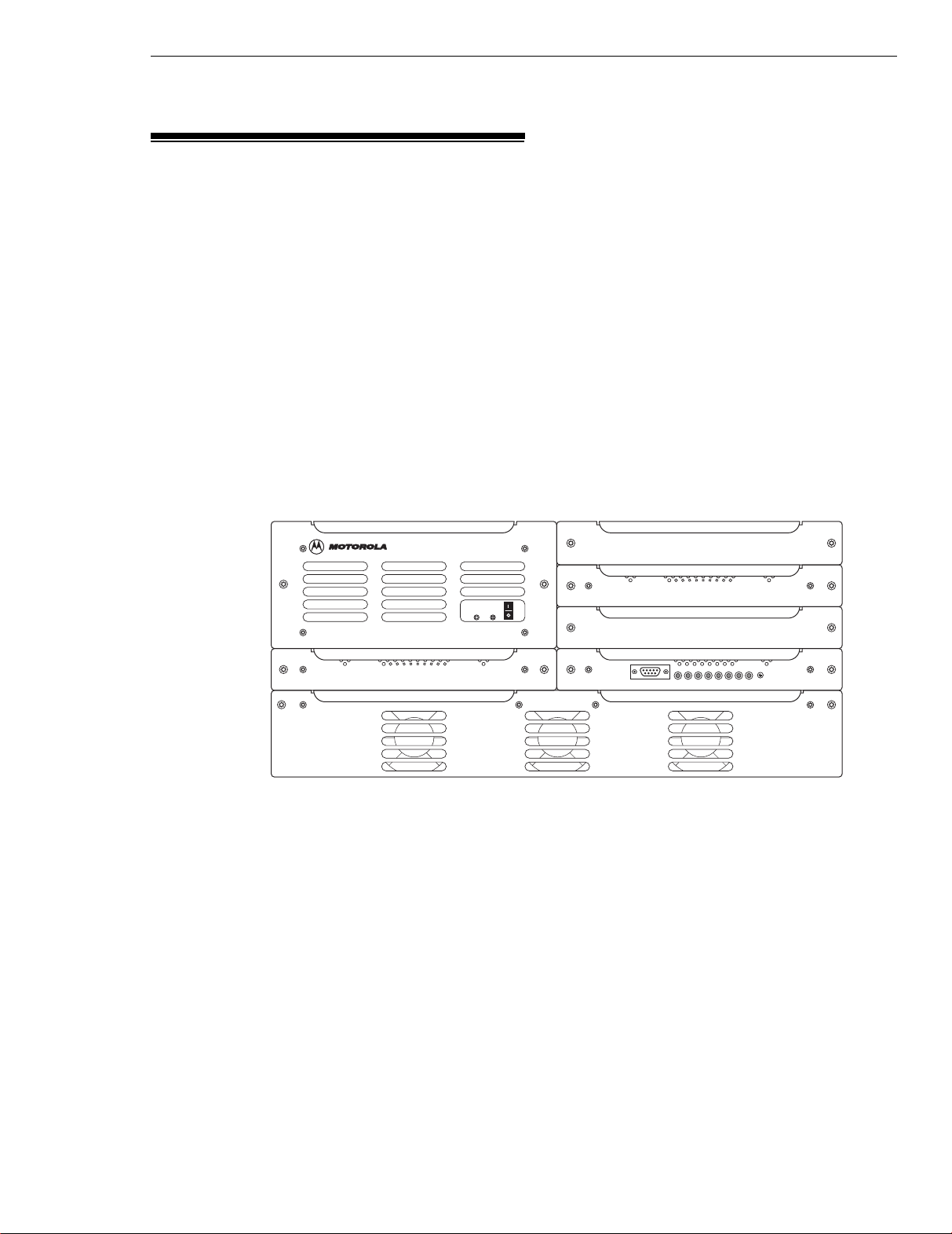
Figure 1
INSERT ONLY IN SLOT RX2 WITH BACKPLANE 0183625X
POWER SUPPLY
LOW NOISE EXCITER
SERVICE ACCESS
Generation 2 Base Radio (Typical)
ENHANCED CONTROL
RESETBR PS EX PA CTL R1 R2 R3
POWER AMPLIFIER
3X RECEIVER
EBTS282
101497JNM
68P80801E35-B 5/1/2002 3
Page 23

Base Radio EBTS System Manual - Vol 2
Generation 2 Single Channel 800 MHz Base Radio Overview
Generation 2 Single Channel Radio Controls and Indicators
The Power Supply and EBRC contain controls and indicators that provide a
means for monitoring various status and operating conditions of the BR, and also
aid in fault isolation. The controls and indicators for both modules are discussed
in the Power Supply and EBRC sections of this chapter.
The Power Supply contains two front panel indicators; the EBRC contains eight
front panel indicators. The Power Supply contains a power switch used to apply
power to the BR. The EBRC contains a RESET switch used to reset the BR.
Generation 2/EBRC Compatibility
Table 2
Exciter R01.00.xx- R01.03.xx SR10.0 or Greater
Exciter R01.04.xx and higher SR9.15 or Greater
Single Receiver R01.00.xx - R01.02.xx SR10.0 or Greater
Single Receiver R01.03.xx and higher SR9.15 or Greater
3X Receiver all versions SR9.15 or Greater
40W Power Amplifier all versions SR9.15 or Greater
70W Power Amplifier all versions SR9.15 or Greater
The Enhanced Base Radio Controller (EBRC) serves as the main controller for the
Base Radio. The EBRC provides signal processing and operational control for
other Base Radio modules. Figure 1 shows a top view of the EBRC module with
the cover removed. The EBRC module consists of two printed circuit boards
(EBRC board and LED display board), a slide-in housing, and associated
hardware.
❐ The EBRC is only compatible with System Software Release SR 9.15 or later.
Any system running a pre-SR 9.15 System Release must be updated to at
least SR 9.15 prior to installation.
❐ The EBRC module is compatible with Legacy Base Radios that support
multiple receiver module assemblies.
❐ The Generation 2 Base Radio is compatible with all versions of power
supplies.
EBRC Compatibility
Module Software Revision System Release
4 68P80801E35-B 5/1/2002
Page 24

EBTS System Manual - Vol 2 Base Radio
Generation 2 Single Channel 800 MHz Base Radio Overview
❐ The Generation 2 Base Radio is compatible with all 800 MHz 70W and 40W
Power Amplifiers.
❐ The EBRC module is only compatible with Legacy Exciter (containing
revision number R1.04.xx and higher) or the Low Noise Exciter.
Determining FRU and Kit Revisions
For Generation 2 BR/EBRC
These commands will return all available FRU and Kit Revision numbers. Use
these to determine installation requirements:
1. Connect one end of the RS-232 cable to the service computer.
2. Connect the other end of the RS-232 cable to the Service Access port, located
on the front panel of the EBRC module.
3. Power on the BR using the front switch on the Power Supply Module. Press
the reset button on the Control Module front panel. At the prompt, hit a
Carriage Return on the service computer to enter the test application mode.
Using the password motorola, log in to the BR.
:> login -ufield
password: motorola
field>
4. Collect revision numbers from the station by typing the
following command:
field> fv -oplatform
field>
5. If all modules return revision numbers of the format “Rxx.xx.xx”, then all
revision numbers are present. In that case, verification requires no further
action. If revision numbers return as blank, or not in the format “Rxx.xx.xx”,
contact your local Motorola representative or Technical Support.
68P80801E35-B 5/1/2002 5
Page 25

Base Radio EBTS System Manual - Vol 2
Generation 2 Single Channel 800 MHz Base Radio Overview
For Legacy Single Channel BR/BRC
1. Connect one end of the RS-232 cable to the service computer.
2. Connect the other end of the RS-232 cable to the STATUS port, located on the
front panel of the BRC.
3. Using the field password, login to the BR.
4. Collect revision numbers from the station by typing the
following commands:
BRC>dekey
BRC>test_mode
BRC>get brc_rev_no
BRC>get rx1_rev_no
BRC>get rx2_rev_no
BRC>get rx3_rev_no
BRC>get pa_rev_no
BRC>get ex_rev_no
(
if BR is 3 branch
)
BRC>
6 68P80801E35-B 5/1/2002
Page 26

EBTS System Manual - Vol 2 Base Radio
Generation 2 Single Channel 800 MHz Base Radio Overview
5. If all modules return revision numbers of the format “Rxx.xx.xx”, then all
revision numbers are present and no further action is required. Log out and
repeat steps 1 through 4 for each additional BR.
If revision numbers were returned as blank or not in the format “Rxx.xx.xx”,
contact your local Motorola representative or Technical Support.
Generation 2 Single Channel BR General Specifications
General specifications for the Generation 2 BR are listed in Table 2.
Table 3
Generation 2 BR General Specifications
Specification Value or Range
Dimensions:
Height
Width
Depth
Operating Temperature 32˚ to 104˚ F (0˚ to 40˚ C)
Storage Temperature -22˚ to 140˚ F (-30˚ to 60˚ C)
Rx Frequency Range:
800 MHz iDEN 806 - 825 MHz
Tx Frequency Range:
800 MHz iDEN 851 - 870MHz
Tx – Rx Spacing:
800 MHz iDEN 45 MHz
Channel Spacing 25 kHz
Frequency Generation Synthesized
Digital Modulation M-16QAM
Power Supply Inputs:
VDC -48 VDC (-41 - 60 VDC)
Diversity Branches Up to 3
5 EIA Rack Units (RU)
19" (482.6 mm)
16.75" (425 mm)
68P80801E35-B 5/1/2002 7
Page 27

Base Radio EBTS System Manual - Vol 2
Generation 2 Single Channel 800 MHz Base Radio Overview
Gen 2 Single Channel BR Transmit Specifications
The Generation 2 BR transmit specifications are listed in Table 4.
Table 4
Transmit Specifications
Specification Value or Range
Average Power Output:
(800 MHz) 40 W PA
(800 MHz) 70 W PA
Transmit Bit Error Rate (BER) 0.01%
Occupied Bandwidth 18.5 kHz
Frequency Stability * 1.5 ppm
RF Input Impedance 50 Ω (nom.)
FCC Designation (FCC Rule Part 90):
(800 MHz Legacy) 40 W PA
(800 MHz Legacy) 70 W PA
(800 MHz Low Noise Exciter) 40 W PA
(800 MHz Low Noise Exciter) 70 W PA
* Stability without site reference connected to station.
5 - 40 W
5- 70 W
ABZ89FC5772
ABZ89FC5763
ABZ89FC5772-A
ABZ89FC5763-A
Gen 2 Single Channel BR Receive Specifications
The receive specifications are listed in Table 5.
Table 5
Receive Specifications
Specification Value or Range
Static Sensitivity †:
800 MHz BR -108 dBm (BER = 8%)
BER Floor (BER = 0.01%) ≥ -80 dBm
IF Frequencies
1st IF (All bands):
2nd IF:
800MHz
Frequency Stability * 1.5 ppm
RF Input Impedance 50 Ω (nom.)
FCC Designation (FCC Rule Part 15):
800 MHz BR ABZ89FR5762
† Measurement referenced from single receiver input port of BR.
* Stability without site reference connected to station.
73.35 MHz (1st IF)
450 kHz (2nd IF)
8 68P80801E35-B 5/1/2002
Page 28

Base Radio EBTS System Manual - Vol 2
Generation 2 Single Channel 800 MHz Base Radio Overview
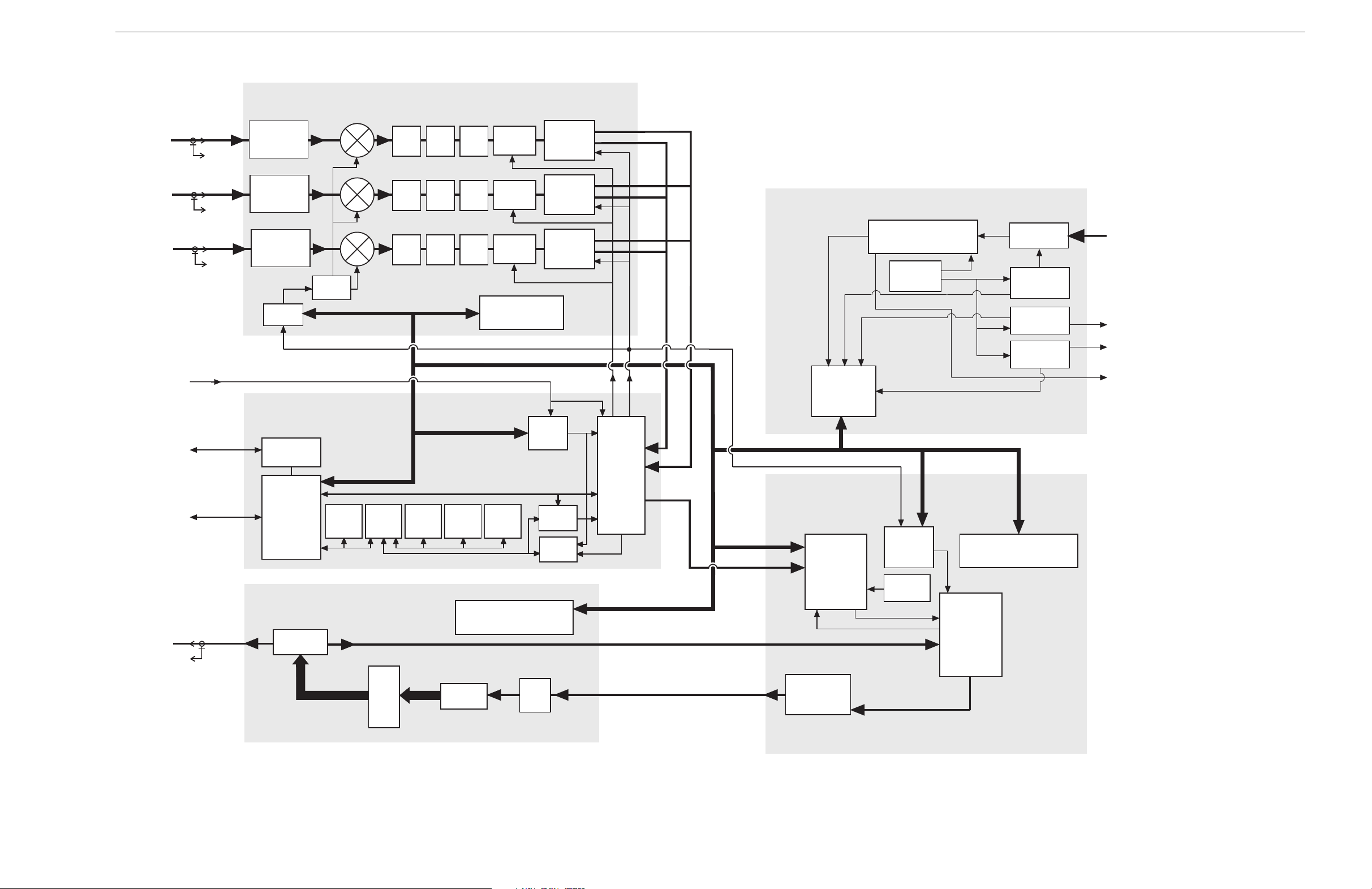
Generation2 Single Channel BR Theory of Operation
The BR operates in conjunction with other site controllers and equipment that are
properly terminated. The following description assumes such a configuration.
Figures 5 shows an overall block diagram of the BR.
Power is applied to the DC Power input located on the BR backplane. The DC
Power input is connected if -48 VDC or batteries are used in the site.
Power is applied to the BR by setting the Power Supply power switch to the ON
position. Upon power-up, the BR performs self-diagnostic tests to ensure the
integrity of the unit. These tests are primarily confined to the EBRC and include
memory and Ethernet verification routines.
After the self-diagnostic tests are complete, the BR reports any alarm conditions
present on any of its modules to the site controller via Ethernet. Alarm conditions
may also be verified locally using service computer and the STATUS port located
on the front of the EBRC.
The software resident in Flash Memory on the EBRC registers the BR with the site
controller via Ethernet. Once registered, the BR software is downloaded via
resident FLASH- or Ethernet and is executed from RAM. Operating parameters
for the BR are included in this download. This software allows the BR to perform
call processing functions.
The BR operates in a TDMA (Time Division Multiple Access) mode. This mode,
combined with voice compression techniques, provides an increased channel
capacity ratio of as much as 6 to 1. Both the receive and transmit signals of the BR
are divided into 6 individual time slots. Each receive slot has a corresponding
transmit slot; this pair of slots comprises a logical RF channel.
The BR uses diversity reception for increased coverage area and improved
quality. The Receiver module within the BR contains up to three receivers. Two
Receivers are used with two-branch diversity sites, and three Receivers are used
with three-branch diversity sites.
All Receivers within a given BR are programmed to the same receive frequency.
The signals from each receiver are fed to the EBRC where a diversity combining
algorithm is performed on the signals. The resultant signal is processed for error
correction and then sent to the site controller via Ethernet with the appropriate
control information regarding its destination.
The transmit section of the BR is comprised of two separate FRUs, the Exciter and
Power Amplifier (PA). Several PA FRUs are available, covering different
applications and power levels; these are individually discussed as applicable in
later subsections.
The Exciter processes the information to transmit from the EBRC in the proper
modulation format. This low level signal is sent to the PA where it is amplified to
the desired output power level. The PA is a continuous keyed linear amplifier. A
power control routine monitors the output power of the BR and adjusts it as
necessary to maintain the proper output level.
10 68P80801E35-B 5/1/2002
Page 29
68P80801E35-B 5/1/2002
27
EBTS System Manual - Vol 2 800/900/1500 MHz Base Radios
Base Radio Overview
POWER AMPLIFIER MODULE
TO/FROM
ETHERNET
ENHANCED
BASE RADIO CONTROLLER
MODULE
EXCITER MODULE
DC POWER SUPPLY MODULE
SERIAL BUS
TO/FROM
STATUS
PORT
(RS-232)
16.8 MHZ
5 MHZ
SPI BUS
5 MHZ
EXTERNAL
REFERENCE
FINAL
LINEAR
AMPS
SPLITTER
LINEAR
DRIVER
ADDRESS DECODE,
MEMORY, A/D CONVERTER
ADDRESS DECODE,
MEMORY, A/D CONVERTER
FROM
RFDS
(RECEIVER
ANTENNA)
#3
3X RECEIVER MODULE
MIXER
DSP BUS
LPF/
PRESELECT/
PREAMP/
IMAGE FILTER
VCO/
SYNTH
ADDRESS DECODE,
MEMORY,
A/D CONVERTER
PLL/
VCO
SPI BUS
2.1 MHZ
COMBINER
LINEAR RF
AMPLIFIER
EXCITER
IC
IF IN IF OUT
TRANLIN
IC
INPUT FILTER
BOARD
CLOCK
GENERATOR
CIRCUITRY
START-UP
INVERTER
CIRCUITRY
133 KHZ
267 KHZ
+14.2 V
INVERTER
CIRCUITRY
133 KHZ
DIAGNOSTICS
CIRCUITRY
+14.2 VDC
TO BACKPLANE
+5 VDC
TO BACKPLANE
+28 VDC
TO BACKPLANE
EXTERNAL
DC INPUT
41 - 60 VDC
RF OUT
SPI BUS
SPI BUS
SPI BUS
SPI BUS
2.1 MHZ
SPI BUS
DATA/CLOCK
DATA/CLOCK
RF IN
RF OUT
RF FEEDBACK
FEEDBACK IN
DIGITAL
ATTEN.
CIRCUIT
AGC
SPI BUS
RF IN
CUSTOM
RECEIVER
IC
EBTS284
053001JNM
TO
RFDS
(TRANSMIT
ANTENNA)
MAIN INVERTER
CIRCUITRY
+5 V
INVERTER
CIRCUITRY
FROM
RFDS
(RECEIVER
ANTENNA)
#2
MIXER
DSP BUS
LPF/
PRESELECT/
PREAMP/
IMAGE FILTER
RF IN
DIGITAL
ATTEN.
CIRCUIT
CUSTOM
RECEIVER
IC
FROM
RFDS
(RECEIVER
ANTENNA)
#1
MIXER
DSP BUS
LPF/
PRESELECT/
PREAMP/
IMAGE FILTER
RF IN
DIGITAL
ATTEN.
CIRCUIT
CUSTOM
RECEIVER
IC
BAND
PASS
FILTER
BAND
PASS
FILTER
BAND
PASS
FILTER
IF
AMP
IF
AMP
IF
AMP
BAND
PASS
FILTER
BAND
PASS
FILTER
BAND
PASS
FILTER
3-WAY
SPLITTER
NOTES:
1. 2-Branch systems must have a 50Ω load (P/N 5882106P03) installed on Antenna Port #3.
2. Set the RX_FRU_CONFIG parameter as follows:
2-Branch Systems: 12
3-Branch Systems: 123
3. Where two frequencies are given, frequency without parentheses applies to 800 MHz BR only and frequency with parentheses applies to 900 MHz BR only.
970 MHZ
(1025 MHZ)
VCO/SYNTH
FREQUENCY
DOUBLER
237 MHZ
(180.6 MHZ)
VCO
SDRAM
IO
LATCHES
EEPROMFLASHBUFFERS
HOST
µ
P
ETHERNET
INTERFACE
RECEIVE
DSP
TRANSMIT
DSP
TISIC
1PPS &
SLOT
TIMING
Figure 5
Generation 2 Single Channel 800 MHz Base Radio Functional Block Diagram
Page 30

Base Radio Controllers
Overview
This chapter provides information on Base Radio Controllers (BRCs):
Chapter Topic Page Description
Enhanced Base Radio Controller 2 Includes information on the Enhanced Base Radio
900 MHz QUAD Channel Base Radio
Controller
800 MHz QUAD Channel Base Radio
Controller
800/900/1500 MHz Legacy Base Radio
Controller
15 Provides an 900 MHz QUAD Channel BRC Controls and
25 Provides an overview, 800 MHz QUAD Channel BRC
35 Provides an overview, outline of controls and indications as
Controller’s Controls and Indications and Theory of
Operation
Indications as well as the controller’s Theory of Operation
Controls and Indications as well as the controller’s Theory of
Operation
well as the controller’s Theory of Operation
FRU Number to Kit Number Cross Reference
Base Radio Controller (BRC) Field Replaceable Units (FRUs) are available for the
iDEN EBTS. The FRU contains the BRC kit and required packaging. Table 1
provides a cross reference between BRC FRU numbers and kit numbers.
Table 1
Description FRU Number Kit Number
Single Channel 800/900/1500 MHz Base Radio
Controller
Single Channel Base Radio Controller
(1500 MHz MCI)
Enhanced Base Radio Controller DLN6446 CLN1653
QUAD Channel 900 MHz Exciter/BR Controller DLN1203
QUAD Channel 800 MHz Exciter/BR Controller CLN1497 CLF1560
FRU Number to Kit Number Cross Reference
TLN3334 CLN1469
TLN3425 CLN1472
Global Telecommunications Solutions Sector
68P80801E35-B 5/1/2002 1
1301 E. Algonquin Road, Schaumburg, IL 60196
Page 31

Base Radio Controllers EBTS System Manual - Vol 2
Enhanced Base Radio Controller
Enhanced Base Radio Controller
Enhanced Base Radio Controller Overview
Generation 2 BR/EBRC Compatibility
Table 2
The Enhanced Base Radio Controller (EBRC) serves as the main controller for the
Base Radio. The EBRC provides signal processing and operational control for
other Base Radio modules. Figure 1 shows a top view of the EBRC with the cover
removed. The EBRC module consists of two printed circuit boards (EBRC board
and LED display board), a slide-in housing, and associated hardware.
❐ The EBRC is only compatible with System Software Release SR 9.15 or
❐ The EBRC is compatible with Legacy Base Radios that support multiple
❐ The Generation 2 Base Radio is compatible with all versions of power
EBRC Compatibility
Module Software Revision Compatible
Exciter R01.00.xx- R01.03.xx SR 10.0 or Greater
Exciter R01.04.xx and higher SR 9.15 or Greater
Single Receiver R01.00.xx - R01.02.xx SR 10.0 or Greater
Single Receiver R01.03.xx and higher SR 9.15 or Greater
3X Receiver all versions SR 9.15 or Greater
40W Power Amplifier all versions SR 9.15 or Greater
70W Power Amplifier all versions SR 9.15 or Greater
newer. Any system running a pre-SR 9.15 System Release must be updated
to at least SR 9.15 prior to installation.
receiver module assemblies.
supplies.
2 68P80801E35-B 5/1/2002
Page 32

EBTS System Manual - Vol 2 Base Radio Controllers
Enhanced Base Radio Controller
Determining FRU and Kit Revisions
For Generation 2 BR/EBRC
These commands will return all available FRU and Kit Revision numbers. Use
these to determine installation requirements:
1. Connect one end of the RS-232 cable to the service computer.
2. Connect the other end of the RS-232 cable to the Service Access port, located
on the front panel of the EBRC module.
3. Power on the BR using the front switch on the Power Supply Module. Press
the reset button on the Control Module front panel. At the prompt, hit a
Carriage Return on the service computer to enter the test application mode.
Using the password motorola, log in to the BR.
:> login -ufield
password: motorola
field>
4. Collect revision numbers from the station by typing the
following command:
field> fv -oplatform
field>
5. If all modules return revision numbers of the format “Rxx.xx.xx”, then all
revision numbers are present. In that case, verification requires no further
action. If revision numbers return as blank, or not in the format “Rxx.xx.xx”,
contact your local Motorola representative or Technical Support.
For Legacy Single Channel BR/BRC
1. Connect one end of the RS-232 cable to the service computer.
2. Connect the other end of the RS-232 cable to the STATUS port, located on the
front panel of the BRC.
3. Using the field password, login to the BR.
68P80801E35-B 5/1/2002 3
Page 33

Base Radio Controllers EBTS System Manual - Vol 2
Enhanced Base Radio Controller
4. Collect revision numbers from the station by typing the
following commands:
BRC>dekey
BRC>test_mode
BRC>get brc_rev_no
BRC>get rx1_rev_no
BRC>get rx2_rev_no
BRC>get rx3_rev_no
BRC>get pa_rev_no
BRC>get ex_rev_no
BRC>
5. If all modules return revision numbers of the format “Rxx.xx.xx”, then all
revision numbers are present and no further action is required. Log out and
repeat steps 1 through 4 for each additional BR.
If revision numbers were returned as blank or not in the format “Rxx.xx.xx”,
contact your local Motorola representative or Technical Support.
(
if BR is 3 branch
)
EBRC Description
The EBRC memory contains the operating software and codeplug. The software
defines BR operating parameters, such as output power and operating frequency.
The EBRC connects to the Base Radio backplane with one 96-pin Euro connector
and one blindmate RF connector. Two Torx screws secure the EBRC in the Base
Radio chassis.
Figure 1 shows a top view of the EBRC (model CLN1653) with the cover removed.
The EBRC module contains the main board, CLN7428 and LED board, CLN7208.
4 68P80801E35-B 5/1/2002
Page 34

EBTS System Manual - Vol 2 Base Radio Controllers
Enhanced Base Radio Controller
Figure 1
Enhanced Base Radio Controller, version CLN1653 (with cover removed)
68P80801E35-B 5/1/2002 5
Page 35

Base Radio Controllers EBTS System Manual - Vol 2
Enhanced Base Radio Controller
Enhanced Base Radio Controller Controls and Indicators
The EBRC monitors the functions of other Base Radio modules. The LEDs on the
front panel indicate the status of EBRC-monitored modules. The CTL LED on the
front panel light momentarily on initial BR power-up and on BR resets. Figure 2
shows the front panel of the EBRC.
Figure 2
SERVICE ACCESS
EBRC (Front View)
ENHANCED CONTROL
RESETBR PS EX PA CTL R1 R2 R3
EBTS316g
06701SJW
Indicators
Table 3 lists and describes the EBRC LEDs.
Table 3
EBRC Indicators
LED Color Module
Monitored
BR Green BR Solid (on) Station is keyed
PS Red Power
Supply
EX Red Exciter Solid (on) FRU failure indication - Exciter has a
PA Red Power
Amplifier
Condition Indications
Flashing (on) Station is not keyed
Off Station is out of service or power is
removed
Solid (on) FRU failure indication - Power Supply
has a major alarm and is out of service
Flashing (on) Power Supply has a minor alarm and
may be operating at reduced
performance
Off Power Supply under normal operation
(no alarms)
major alarm and is out of service
Flashing (on) Exciter has a minor alarm and may be
operating at reduced performance
Off Exciter under normal operation
(no alarms)
Solid (on) FRU failure indication - PA has a major
alarm and is out of service
Flashing (on) PA has a minor alarm and may be
operating at reduced performance
Off PA under normal operation (no
alarms)
6 68P80801E35-B 5/1/2002
Page 36

EBTS System Manual - Vol 2 Base Radio Controllers
Enhanced Base Radio Controller
Table 3
EBRC Indicators (Continued)
LED Color Module
Monitored
CTL Red Controller Solid (on) FRU failure indication - BRC has a
R1
R2
R3
Red Receiver #1,
#2, or #3
Condition Indications
major alarm and is out of service.
NOTE:
Flashing (on) BRC has a minor alarm and may be
operating at reduced performance
Off BRC under normal operation (no
alarms)
Solid (on) FRU failure indication - Receiver (#1,
#2, or #3) has a major alarm and is out
of service
Flashing (on) Receiver (#1, #2, or #3) has a minor
alarm and may be operating at
reduced performance
Off Receiver (#1, #2, or #3) under normal
operation (no alarms)
Controls
Table 4 lists the controls and descriptions.
Table 4
EBRC Controls
Control Description
RESET Switch A push-button switch used to manually reset the BR.
STATUS
connector
A 9-pin connector used for connection of a service computer, providing a
convenient means for testing and configuring.
STATUS Connector
Table 5 the pin-outs for the STATUS connector.
68P80801E35-B 5/1/2002 7
Page 37

Base Radio Controllers EBTS System Manual - Vol 2
Enhanced Base Radio Controller
Table 5
Pin-outs for the STATUS Connector
Pin-out Signal
1 not used
2 TXD
3 RXD
4 not used
5 GND
6 not used
7 not used
8 not used
9 not used
8 68P80801E35-B 5/1/2002
Page 38

EBTS System Manual - Vol 2 Base Radio Controllers
Enhanced Base Radio Controller
Enhanced Base Radio Controllers Theory of Operation
Table 6 briefly describes the EBRC circuitry. Figure 15 is a functional block
diagram of the EBRC.
Table 6
EBRC Circuitry
Circuit Description
Host Microprocessor Contains integrated circuits that comprise the central controller
of the EBRC and station
Non-Volatile Memory Consists of:
• FLASH containing the station operating software
• EEPROM containing the station codeplug data
Volatile Memory Contains SDRAM to store station software used to execute
commands.
Ethernet Interface Provides the EBRC with a 10Base2 Ethernet communication
port to network both control and compressed voice data
RS-232 Interface Provides the EBRC with an RS-232 serial interface
Digital Signal Processors Performs high-speed modulation/demodulation of
compressed audio and signaling data
TISIC Contains integrated circuits that provide timing reference
signals for the station
TX Reclock Contains integrated circuits that provide highly stable,
reclocked transmit signals and peripheral transmit logic
Station Reference Circuitry Generates the 16.8 MHz and 48 MHz reference signals used
throughout the station
Input Ports Contains 16 signal input ports that receive miscellaneous
inputs from the BR
Output Ports Contains 40 signal output ports, providing a path for sending
miscellaneous control signals to circuits throughout the BR
Remote Station Shutdown Provides software control to cycle power on the BR
MPC860 Host Microprocessor
The MPC860 host microprocessor is the main controller for the BR. The processor
operates at a 50-MHz clock speed. The processor controls Base Radio operation
according to station software in memory. Station software resides in FLASH
memory. For normal operation, the system transfers this software to non-volatile
memory. An EEPROM contains the station codeplug.
NOTE
At BR power-up, the EBRC LED indicates a major
alarm. This indication continues until BR software
achieves a predetermined state of operation.
Afterward, the software turns off the EXBRC LED.
68P80801E35-B 5/1/2002 9
Page 39

Base Radio Controllers EBTS System Manual - Vol 2
Enhanced Base Radio Controller
Serial Communication Buses
The microprocessor provides a general-purpose SMC serial management
controller bus.
The SMC serial communications bus is an asynchronous RS-232 interface with no
hardware handshake capability. The BRC front panel includes a nine-pin, D-type
connector. This connector provides a port where service personnel may connect a
service computer. Service personnel can perform programming and maintenance
tasks via Man-Machine Interface (MMI) commands. The interface between the
SMC port and the front- panel STATUS connector is via EIA-232 Bus Receivers
and Drivers.
Host Processor
The microprocessor incorporates 4k bytes of instruction cache and 4k bytes of
data cache that significantly enhance processor performance.
The microprocessor has a 32-line address bus. The processor uses this bus to
access non-volatile memory and SDRAM memory. Via memory mapping, the
processor also uses this bus to control other BRC circuitry.
The microprocessor uses its Chip Select capability to decode addresses and assert
an output signal. The eight chip-select signals select non-volatile memory,
SDRAM memory, input ports, output ports, and DSPs.
The Host processor...
❐ Provides serial communications between the Host Microprocessor and other
Base Radio modules.
❐ Provides condition signals necessary to access SDRAM.
❐ Accepts interrupt signals from EBRC circuits (such as DSPs).
❐ Organizes the interrupts, based on hardware-defined priority ranking.
❐ The Host supports several internal interrupts from its Communications
Processor Module. These interrupts allow efficient use of peripheral
interfaces.
❐ The Host supports 10 Mbps Ethernet/IEEE 802.3.
❐ Provides a 32-line data bus transfers data to and from EBRC SDRAM and
other BRC circuitry. Buffers on this data bus allow transfers to and from
non-volatile memory, general input and output ports and DSPs.
Non-Volatile Memory
Base Radio software resides in 2M x 32 bits of FLASH memory. The Host
Microprocessor addresses the FLASH memory with 20 of the host address bus’ 32
lines. The host accesses FLASH data over the 32-line host data bus. A
host-operated chip-select line provides control signals for these transactions.
The FLASH contains the operating system and application code. The system
stores application code in FLASH for fast recovery from reset conditions.
Application code transfers from network or site controllers may occur in a
10 68P80801E35-B 5/1/2002
Page 40

EBTS System Manual - Vol 2 Base Radio Controllers
Enhanced Base Radio Controller
background mode. Background mode transfers allow the station to remain
operational during new code upgrades.
The data that determines the station personality resides in a 32K x eight bit
codeplug EEPROM. The microprocessor addresses the EEPROM with 15 of the
host address bus’ 32 lines. The host accesses EEPROM data with eight of the data
bus’ 32 lines. A host-operated chip-select line provides control signals for these
transactions.
During the manufacturing process, the factory programs the codeplug’s default
data. The BRC must download field programming data from network and site
controllers. This data includes operating frequencies and output power level. The
station permits adjustment of many station parameters, but the station does not
store these adjustments. Refer to the Software Commands chapter for additional
information.
Volatile Memory
Each BRC contains 8MB x 32 bits of SDRAM. The BRC downloads station
software code into SDRAM for station use. SDRAM also provides short-term
storage for data generated and required during normal operation. SDRAM is
volatile memory. A loss of power or system reset destroys SDRAM data.
The system performs read and write operations over the Host Address and Data
buses. These operations involve column and row select lines under control of the
Host processor’s DRAM controller. The Host address bus and column row signals
sequentially refresh SDRAM memory locations.
Ethernet Interface
The Host processor’s Communications Processor Module (CPM) provides the
Local Area Network (LAN) Controller for the Ethernet Interface. The LAN
function implements the CSMA/CD access method, which supports the IEEE
802.3 10Base2 standard.
The LAN coprocessor supports all IEEE 802.3 Medium Access Control, including
the following:
❐ framing
❐ preamble generation
❐ stripping
❐ source address generation
❐ destination address checking
The PCM LAN receives commands from the CPU.
The Ethernet Serial Interface works directly with the CPM LAN to perform the
following major functions:
❐ 10 MHz transmit clock generation (obtained by dividing the 20 MHz signal
provided by on-board crystal)
❐ Manchester encoding/decoding of frames
68P80801E35-B 5/1/2002 11
Page 41

Base Radio Controllers EBTS System Manual - Vol 2
Enhanced Base Radio Controller
❐ electrical interface to the Ethernet transceiver
An isolation transformer provides high-voltage protection. The transformer also
isolates the Ethernet Serial Interface (ESI) and the transceiver. The pulse
transformer has the following characteristics:
❐ Minimum inductance of 75 µH
❐ 2000 V isolation between primary and secondary windings
❐ 1:1 Pulse Transformer
The Coaxial Transceiver Interface (CTI) is a coaxial cable line driver and receiver
for the Ethernet. CTI provides a 10Base2 connection via a coaxial connector on the
board. This device minimizes the number of external components necessary for
Ethernet operations.
A DC/DC converter provides a constant voltage of -9 Vdc for the CTI from a
3.3 Vdc source.
The CTI performs the following functions:
❐ Receives and transmits data to the Ethernet coaxial connection
❐ Reports any collision that it detects on the coaxial connection
❐ Disables the transmitter when packets are longer than the legal length
(Jabber Timer)
Digital Signal Processors
The BRC includes two Receive Digital Signal Processors (RXDSPs) and a Transmit
Digital Signal Processor (TXDSP). These DSPs and related circuitry process
compressed station transmit and receive audio or data. The related circuitry
includes the TDMA Infrastructure Support IC (TISIC) and the TISIC Interface
Circuitry. The DSPs only accept input and output signals in digitized form.
The RXDSP inputs are digitized receiver signals. The TXDSP outputs are digitized
voice audio and data (modulation signals). These signals pass from the DSP to the
Exciter portion of the EXBRC. DSPs communicate with the Microprocessor via an
eight-bit, host data bus on the host processor side. For all DSPs, interrupts drive
communication with the host.
The RXDSP operates from an external 16.8 MHz clock, provided by the local
station reference. The RXDSP internal operating clock signal is 150MHz,
produced by an internal Phase-Locked Loop (PLL).
The RXDSP accepts digitized signals from the TISIC device through the RxDSP
parallel bus. The RXDSP supports a single carrier (single 3 branch receiver) digital
data input.
The RXDSP accesses its DSP program and signal-processing algorithms in 128k
words of internal memory. The RXDSP communicates with the host bus on an
8-bit interface.
Additionally, a serial control path connects the two RXDSPs and the TXDSP. The
Synchronous Communications Interface (SCI) port facilitates this serial control
path.
12 68P80801E35-B 5/1/2002
Page 42

EBTS System Manual - Vol 2 Base Radio Controllers
Enhanced Base Radio Controller
For initialization and control purposes, the RXDSP connects to the TISIC device.
The TXDSP operates at an external clock speed of 16.8 MHz, provided by the
EBRC local station reference. The TXDSP internal operating clock is 150MHz,
produced by an internal Phase Lock Loop (PLL).
The TXDSP sends one carrier of digitized signal to the TISIC to reformat the date
before sending it to the exciter. The exciter converts the digital signal to analog.
The TXDSP contains its own, internal address and data memory. The TXDSP can
store 128k words of DSP program and data memory. An eight-bit interface
handles TXDSP-to-host bus communications.
TISIC
The TISIC controls internal DSP operations. This circuit provides the following
functions:
❐ For initialization and control, interfaces with the RXDSP via the DSP
address and data buses.
❐ Accepts a 16.8 MHz signal from Station Reference Circuitry.
❐ Accepts a 5 MHz signal, modulated with one pulse per second (1 PPS) from
the site reference.
❐ Demodulates the 1 PPS from the modulated 5 MHz signal
❐ Outputs a 1 PPS signal and a windowed version of this signal for network
timing alignment.
❐ Outputs a 2.1 MHz reference signal used by the Exciter and Receiver(s).
❐ Generates 15 ms and 7.5 ms ticks. (These ticks synchronize to the 1 PPS time
mark. The system decodes the time mark from the site reference. Then the
system routes the reference to the TXDSP and RXDSP.)
❐ Provides a 4.8 MHz reference signal. This signal is used by the Exciter to
clock data into the TRANLIN
❐ Accepts differential data from the Receiver(s) (Rx through Rx3) via the
interface circuitry.
❐ Transmits serial control data to the Receiver(s) (Rx through Rx3) via the
serial data bus.
❐ Accepts and formats differential data from the TXDSP for transmission to
the Exciter via interface circuitry.
❐ Generates the Receiver SSI (RxSSI) frame sync interrupt for the RxDSP.
Station Reference Circuitry
The Station Reference Circuitry is a phase-locked loop (PLL). This PLL consists of
a high-stability, Voltage-Controlled, Crystal Oscillator (VCXO) and a PLL IC. GPS
output from the iSC connects to the 5 MHz/1 PPS BNC connector on the BR
backplane. Wiring at this connector routes signals to EXBRC station reference
circuitry.
The PLL compares the 5 MHz reference frequency to the 16.8 MHz VCXO output.
Then the PLL generates a DC correction voltage. The PLL applies this correction
68P80801E35-B 5/1/2002 13
Page 43

Base Radio Controllers EBTS System Manual - Vol 2
Enhanced Base Radio Controller
voltage to the VCO through an analog gate. The analog gate closes when three
conditions coexist: (1) The 5 MHz tests stable. (2) The PLL IC is programmed. (3)
Two PLL oscillator and reference signal output alignments occur.
A loss in the 5MHz / 1PPS signal causes the control voltage enable switch to
open. This complex PLL control allows the BR to maintain 16.5 MHz capability
during short disconnects (of approximately one minute) of the 5 MHz / 1 PPS
signal. (For example, during 5 MHz / 1 PPS cable maintenance work.)
When the gate enables, the control voltage from the PLL can adjust the
high-stability VCXO frequency. The adjustment can achieve a stability nearly
equivalent to that of the external, 5 MHz frequency reference.
The correction voltage from the PLL continuously adjusts the VXCO frequency.
The VXCO outputs a 16.8 MHz clock signal. The circuit applies this clock signal to
the receiver, and TISIC.
The TISIC divides the 16.8 MHz signal by seven, and outputs a 2.1 MHz signal.
This output signal then becomes the 2.1 MHz reference for the Exciter and
Receiver(s).
Input Ports
One general-purpose input register provides for EBRC and station circuit input
signals. The register has 16 input ports. The Host Data Bus conveys input register
data to the Host Microprocessor. Typical inputs include 16.8 Station Reference
Circuitry status outputs and reset status outputs.
Output Ports
Two general-purpose output registers distribute control signals from the Host
Microprocessor to the BRC and station circuitry. One register has 32 output ports
and the other register has 8 output ports. Control signal distribution occurs over
the backplane. The Host Data Bus drives the output ports’ latched outputs.
Typical control signals include front-panel LED signals and SPI peripheral enable
and address lines.
Remote Station Shutdown
The EBRC contains power supply shutdown circuitry. This circuitry can send a
shutdown pulse to the Base Radio Power Supply. BRC software generates the
shutdown control pulse.
After receiving a shutdown pulse, the power supply turns off BR power. Shut
down power sources include 3.3, 5.1, 28.6 and 14.2 Vdc sources throughout the
BR. Due to charges retained by BR storage elements, power supply voltages may
not reach zero. The shutdown only assures that the host processor enters a
power-on-reset state.
A remote site uses the shutdown function to perform a hard reset of all BR
modules.
14 68P80801E35-B 5/1/2002
Page 44

68P80801E35-B 5/1/2002
51
EBTS System Manual - Vol 2 800/900/1500 MHz Base Radios
Base Radio Controller
Figure 15
Enhanced Base Radio Controller Functional Block Diagram
(Sheet 1 of 2)
Enhanced Base Radio Controller
Functional Block Diagram
Model CLN1653A
LED
CONTROL
LINES
HOST
LATCH
P0 OUT
FRONT PANEL LEDS
12
BASE
RADIO
POWER
SUPPLY
EXCITER
PA CTL RX1 RX2 R3
5MHZ_1PPS
BASE RADIO
INPUT
5MHZ
1PPS
G
A
T
I
N
G
STATION REFERENCE CIRCUITRY
SYNTHESIZER
IC / CIRCUITRY
SPI
BUS
PHASE
DETECTION/
FILTERING/
CONTROL
DISCONNECT/
CONNECT
CONTROL
STEARING
LINE
HIGH
STABILITY
VCXO
16.8 MHZ
28V
P0_OUT
REMOTE STATION
SHUTDOWN CIRCUITRY
SHUTDOWN
CIRCUITRY
SHUTDOWN
(TO POWER
SUPPLY)
Page 45

52
68P80801E35-B 5/1/2002
800/900/1500 MHz Base Radios EBTS System Manual - Vol 2
Base Radio Controller
Figure 16
Enhanced Base Radio Controller Functional Block Diagram
(Sheet 2 of 2)
EnhancedBase Radio Controller
Functional Block Diagram
Model CLN1653A
FRONT PANEL
RESET
5MHZ
1PPS
SERIAL MANAGEMENT CONTROLLER (SMC2)
2
SCC1
HOST
MICRO-
PROCESSOR
ETHERNET
SERIAL
INTERFACE
ETHERNET
SERIAL
8
CS2
CS3
INTERFACE
SERIAL PERIPHERAL INTERFACE
HOST ADDRESS BUS
GPLA0, A[8,9,17,18,20:29],RAS,CAS,WE
SDRAM
4M x 16
CLSN
RCV RX
ISOLATION
TRANSFORMER
TRMT TX
3
DRAM MEMORY
D[0:15]
SDRAM
4M x 16
EIA-232
BUS
RECEIVERS/
DRIVERS
ETHERNET INTERFACE
CD
BUFFER
D[0:15]
2
TRANSCEIVER
3
A[0:7]
STATUS PORT
(9 PIN D CONNECTOR
ON BRC FRONT PANEL)
SPI
BUS
A[10:31]
16
EXTENDED HOST
BUS BUFFERS
BUFFER
BUFFER
16
BUFFER
RX1 SERIAL DATA
DATA CLOCK 1
RX2 SERIAL DATA
DATA CLOCK 2
RX3 SERIAL DATA
DATA CLOCK 3
10BASE2
COAX
SPI BUS
TO/FROM
STATION MODULES
16
MA[21:0]
16
16.8MHZ
DSP_A[31:24]
DIFFERENTIAL
TO SINGLE END
DIFFERENTIAL
TO SINGLE END
DIFFERENTIAL
TO SINGLE END
RECEIVE
DIGITAL
SIGNAL
PROCESSOR
(RX DSP 1)
1 PPS TIMING, CONTROL/ SLOT TIMING/RESET
DIGITAL SIGNAL PROCESSING
CIRCUITRY
HOST-DSP BUFFERED ADDRESS BUS
HOST-DSP BUFFERED DATA BUS
D[0, 23]
A[0:5]
NETWORKED
SCI
D[0, 8:23]
TISIC
AGC
BUFFER/
SPLITTER
SERIAL CONTROL DATA
TO RECEIVER 1
SERIAL CONTROL DATA
TO RECEIVER 2
SERIAL CONTROL DATA
TO RECEIVER 3
AGC TO
4
ALL RECEIVERS
2.1 MHz
TO EXCITER
AND RECEIVERS
CS4
50 MHZ
CLOCK
P0_IN
STATUS BUS
STATION MODULES
FROM
SDRAM
4M x 16
D[0:31]
MA[2:21]
CS0
CS1
FLASH
1M x 16
FLASH
1M x 16
NON-VOLATILE MEMORY
D[16:31]
HOST DATA BUS
HOST BUFFERED ADDRESS BUS
MA[2:21]
MD[0:15]
MD[16:31]
SDRAM
4M x 16
D[16:31]
FLASH
1M x 16
FLASH
1M x 16
MD[16:31]
MD[0:15]
D[0:31]
D[0:7]
MA[0:14]
EEPROM
32k x 8
16
16
MD[24:31]
BUFFER
BUFFER
BUFFER
8
16
MD[31:0]
16
DSP_D[31:24]
P0_IN
BUFFER
MD[16,17,20-24,28-31]
EXPANDED STATUS INPUT
AND OUTPUT CONTROL CIRCUITRY
HOST BUFFERED DATA BUS
MD[0:32]
P0_OUT
LATCH
MD[24:31]
P1_OUT
LATCH
TRANSMIT
DIGITAL
SIGNAL
PROCESSOR
(TX DSP)
32
8
40
TRANSMIT
SERIAL
DATA
3
BUS
SINGLE END
TO DIFFERENTIAL
SERIAL DATA AND
CLOCK TO EXCITER
P0_OUT/P1_OUT
CONTROL BUS
TO
STATION MODULES
Page 46

Overview
Base Radio Exciter
This chapter provides technical information for the Exciter (EX).
Section Page Description
800 Legacy MHz Exciter –
TLN3337; 900 MHz Exciter –
CLN1357; 1500 MHz Exciter –
TLN3428
Low Noise 800 MHz Exciter 8 Describes the functions and characteristics of the
QUAD Channel 900 MHz
Exciter
QUAD Channel 800 MHz
Exciter
3 Describes the functions and characteristics of the
Exciter module for the single channel Base Radio
(BR).
Exciter module for the Low Noise Exciter for the
Generation 2 Base Radio (Gen2 BR).
12 Describes the functions and characters of the 900
MHz QUAD Channel Base Radio (BR)
16 Describes the functions and characteristics of the
Exciter module for the 800 MHz QUAD channel
Base Radio (BR).
FRU Number to Kit Number Cross Reference
Exciter Field Replaceable Units (FRUs) are available for the iDEN EBTS. The FRU
contains the Exciter kit and required packaging. Table 1 provides a cross reference
between Exciter FRU numbers and kit numbers.
Table 1
FRU Number to Kit Number Cross Reference
Description FRU Number Kit Number
Single Channel Exciter (800 MHz) TLN3337 CLF1490
Single Channel Exciter (900 MHz) CLN1357 CLF1500
Single Channel Exciter (1500 MHz) TLN3428 CTX1120
QUAD Channel 900 MHz Exciter/
Base Radio Controller)
QUAD Channel 800 MHz Exciter/
Base Radio Controller
LNODCT (Low Noise Offset Direct
Conversion Transmit) Exciter (800
MHz)
CLN1497 CLF6452
CLN1497 CLF1560
TLN3337 CLF1789
Global Telecommunications Solutions
68P80801E35-B 5/1/2002 1
1301 E. Algonquin Road, Schaumburg, IL 60196
Page 47

EBTS System Manual - Vol 2 Base Radio Exciter
800 Legacy MHz Exciter – TLN3337; 900 MHz Exciter – CLN1357; 1500 MHz Exciter – TLN3428
passed through the low-pass loop filter to the 970 MHz Voltage Controlled
Oscillator (VCO) circuit (1025 MHz VCO for 900 MHz BR).
970/1025 MHz Voltage Controlled Oscillator (VCO)
The 970 MHz VCO (1025 MHz for 900 MHz BR, 700 MHz for 1500 MHz BR)
generates the second injection frequency for the Exciter IC.
The VCO requires a very low-noise DC supply voltage of +10 VDC for proper
operation. The oscillator is driven by a Super Filter that contains an ultra
low-pass filter. The Super Filter obtains the required low-noise output voltage for
the oscillator.
The output of the oscillator is tapped and sent to the VCO Feedback Filter. This
feedback signal is supplied to the Synthesizer circuitry for the generation of
correction pulses.
The untapped output of the 970 (or 1025) MHz VCO is sent to the second LO
injection circuitry.
236/237/180.6 MHz Voltage Controlled Oscillator (VCO)
The 237 MHz VCO (180.6 MHz for 900 MHz BR, 236 MHz for 1500 MHz BR)
provides a LO signal to Tranlin IC for the first up-conversion and for the second
down-conversion of the feedback signal. The synthesizer and divide by 2
circuitry within the Tranlin IC set the first IF to 118.5 MHz (90.3 MHz for 900 MHz
BR).
Regulator Circuity
This circuit generates three regulated voltages of +5 VDC, +10 VDC, and +11.8
VDC. All voltages are obtained from the +14.2 VDC backplane voltage. These
voltages are used to power various ICs and RF devices of the Exciter.
Linear RF Amplifier Stages
This circuitry is used to amplify the RF signal from the Exciter IC to an
appropriate level for input to the PA.
Automatic Gain Control (AGC) (1500 MHz only)
The Automatic Gain Control (AGC) circuit controls the output gain of the
transmitter (Exciter and Power Amplifier modules) so that constant forward gain
of the RF amplifier stages is maintained. This is accomplished through the
comparison of feedback signals from the Power Amplifier and the first amplifier
stage of the Exciter.
The output of the differential amplifiers is used to adjust the Attenuator and
Image Filter.
68P80801E35-B 5/1/2002 7
Page 48

Base Radio Exciter EBTS System Manual - Vol 2
Low Noise 800 MHz Exciter
Low Noise 800 MHz Exciter
LNODCT (Low Noise Offset Direct Conversion Transmit) 800 MHz Exciter Overview
The Low Noise Exciter and the Power Amplifier (PA) provide the transmitter
functions of the Generation 2 Base Radio. The Low Noise Exciter module consists
of a printed circuit board, a slide in housing, and associated hardware.
The Low Noise Exciter connects to the Base Radio backplane through a 96-pin
DIN connector and two blindmate RF connectors. Two Torx screws on the front of
the Exciter secure it to the chassis.
There are no controls or indicators on the Exciter. Specifications of the transmitter
circuitry, including the Exciter and PAs, are provided in the Base Radio section of
the manual.
Figure 3 shows the Exciter with the cover removed.
Figure 3
8 68P80801E35-B 5/1/2002
Low Noise 800 MHz Exciter (with cover removed)
Page 49

EBTS System Manual - Vol 2 Base Radio Exciter
Low Noise 800 MHz Exciter
Low Noise Exciter Theory of Operation
Table 3 describes the basic circuitry of the Low Noise Exciter. Figures 9 show the
Low Noise Exciter’s functional block diagram.
Table 3
Exciter Circuitry
Circuit Description
Low Noise IC • Up-converts baseband data to the transmit frequency
• Down-converts the PA feedback signal to baseband
• Uses a baseband Cartesian feedback loop system, necessary
to obtain linearity from the transmitter and avoid
splattering power into adjacent channels
• Performs training functions for proper linearization of the
transmitter
Memory & A/D Converter Serves as the main interface between the synthesizer, Tranlin
Frequency Synthesizer
Circuitry
970 MHz VCO (800 MHz BR) Provides a LO signal to the Low Noise IC, for up-conversion
90.3 MHz VCO (800 MHz BR) Provides a LO signal to Low Noise IC, for the up-conversion
Regulator Circuitry Provides a regulated voltage to various ICs and RF devices
Linear RF amplifier Stages Amplifies the RF signal from the Exciter IC to an appropriate
IC, A/D, and EEPROM on the Exciter, and the BRC via the
SPI bus
• Consists of a phase-locked loop and VCO
• Provides a LO signal to the Low Noise IC for the second
up-conversion and first down-conversion of the feedback
signal from the PA
to the transmit frequency
and for the down-conversion of the feedback signal.
The mixed output becomes the LO signal for Transmit signal
up- and down- conversion
located on the Exciter
level for input to the PA
Memory Circuitry
The memory circuitry is loaded on an EEPROM on the Exciter. The EBRC
performs memory read and write operations via the SPI bus. Information stored
in this memory device includes the kit number, revision number, module-specific
scaling, and correction factors, operations, parameters, and free-form information
(scratch pad) kit number
A/D Converter Circuitry
Analog signals from various areas throughout the Exciter board enter the A/D
converter (A/DC). The A/DC converts these analog signals to digital form. Upon
request of the BRC, A/DC output signals enter the BRC via SPI lines. The
Controller periodically monitors all signals.
Some of the monitored signals include amplifier bias and synthesizer signals.
68P80801E35-B 5/1/2002 9
Page 50

Base Radio Exciter EBTS System Manual - Vol 2
Low Noise 800 MHz Exciter
LNODCT IC Circuitry
The LNODCT IC (Low Noise Offset Direct Conversion Transmit IC) is a main
interface between the Exciter and BRC. The BRC’s Digital Signal Processor (DSP)
sends digitized signals (baseband data) to the Exciter over the DSP data bus.
The differential data clock signal serves as a 2.4 MHz reference signal to the
LNODCT IC’s internal synthesizer. The LNODCT compares the reference signal
with the outputs of Voltage Controlled Oscillators (VCOs). The LNODCT might
sense that a VCO’s output is out of phase or off-frequency. If so, then the
LNODCT sends correction pulses to the VCO. The pulses adjust VCO output,
thereby matching phase and frequency with the reference.
The LNODCT IC up-converts baseband data from the EBRC to the transmit
frequency. The LNODCT IC also down-converts the Transmit signal from the
Power Amplifier to baseband data for cartesian feedback linearization.
The EBRC uses the Serial Peripheral Interface (SPI) bus to communicate with the
LNODCT IC. The SPI bus serves as a general purpose, bi-directional, serial link
between the EBRC and other Base Radio modules, including the Exciter. The SPI
carries control and operational data signals to and from Exciter circuits.
Synthesizer Circuitry
The synthesizer circuit consists of the Phase-Locked Loop (PLL) IC and associated
circuitry. This circuit’s controls the 970 MHz VCO signal. An internal phase
detector generates a logic pulse. This pulse is proportional to the phase or
frequency difference between the reference frequency and loop pulse signal.
The charge pump circuit generates a correction signal. The correction signal
moves up or down in response to phase detector output pulses. The correction
signal passes through the low-pass loop filter. The signal then enters the 970 MHz
Voltage Controlled Oscillator (VCO) circuit.
970 MHz Voltage Controlled Oscillator (VCO)
For proper operation, the VCO requires a very low-noise, DC supply voltage. An
ultra low-pass filter prepares the necessary low-noise voltage and drives the
oscillator.
A portion of the oscillator output signal enters the synthesizer circuitry. The
circuitry uses this feedback signal to generate correction pulses.
The 970 MHz VCO output mixes with the 90.3 MHz VCO output. The result is a
Local Oscillator [LO) signal for the LNODCT IC. The LNODCT uses this LO
signal to up-convert the programmed transmit frequency. The LNODCT also
uses the LO signal to down-convert the PA feedback signal.
10 68P80801E35-B 5/1/2002
Page 51

EBTS System Manual - Vol 2 Base Radio Exciter
Low Noise 800 MHz Exciter
90.3 MHz Voltage Controlled Oscillator (VCO)
The synthesizer within the LNODCT IC sets the 90.3 MHz signal. The 90.3 MHz
VCO provides a LO signal to the LNODCT IC. The LNODCT uses this signal in
up-converting and down-converting the feedback signal.
Regulator Circuitry
The voltage regulators generate three regulated voltages: +3 Vdc, +5 Vdc and
+11.7 Vdc. The regulators obtain input voltages from the +3.3 Vdc and +14.2 Vdc
backplane voltages. The regulated voltages power various ICs and RF devices in
the Exciter.
Linear RF Amplifier Stages
The linear RF amplifiers boost the RF signal from the LNODCT IC. The RF
Amplifier generates an appropriate signal level to drive the PA.
68P80801E35-B 5/1/2002 11
Page 52

68P80801E35-B 5/1/2002
23
EBTS System Manual - Vol 2 800/900/1500 MHz Base Radios
Exciter
DIFFERENTIAL
DATA & CLOCK
FROM
BRC MODULE
ADDRESS BUS
FROM CONTROL
MODULE
SPI BUS
TO/FROM CONTROL
MODULE
ADDRESS DECODE, MEMORY, & A/D
CONVERTER CIRCUITRY
EXCITER IC CIRCUITRY
970 MHZ
VCO CIRCUITRY
SYNTHESIZER
CIRCUITRY
LINEAR RF AMPLIFIER
CIRCUITRY
LO
INJECTION
CIRCUITRY
MEMORY
A/D
CONVERTER
VARIOUS
SIGNALS
TO MONITOR
DC
FILTER
+10 V
CONTROL VOLTAGE
OSCILLATOR
CHARGE
PUMP
2.4 MHZ
VCO FEEDBACK
CHIP
SELECT
SPI BUS (CLOCK & DATA)
FROM BACKPLANE
PHASE
LOCKED
LOOP
IC
R
IN
F
IN
90.3
VCO
CIRCUITRY
OSCILLATOR
BUFFER
AMP
LNODCT IC CIRCUITRY
LNODCT IC
LOW-PASS
LOOP
FILTER
BUFFER
VCO
FEEDBACK
RF OUTPUT
TO PA MODULE
DAC
I
Q
RF FEEDBACK
FROM PA MODULE
BUFFER
AMP
BPF
REGULATOR
CIRCUITRY
+11.7 V
REGULATOR
+14.2 V
FROM
BACKPLANE
+3 V
SOURCE
+11.7 V
SOURCE
+5 V
SOURCE
+5 V
REGULATOR
+3 V
REGULATOR
(U3702)
EBTS283LN
080601JNM
NOTE: Where two frequencies are given, frequency without parentheses applies to 800 MHz BR only and frequency with parentheses applies to 900 MHz BR only.
+5.0 V FROM BACKPLANE
PLD
Figure 8
Low Noise Exciter Functional Block Diagram
Page 53

Overview
Power Amplifier (PA)
This section provides technical information for the Power Amplifier (PA).
Section Page Description
Power Amplifer Overview 1 Describes the the various Base Radio Power
PA Theory of Operation 9 Describes the various modules and functions for
40W - 800 MHz PA
Functional Block Diagram
(Sheet 1 of 1)
70W - 800 MHz PA
Functional Block Diagram
(Sheet 1 of 1)
60W - 900 MHz PA
Functional Block Diagram
(Sheet 1 of 1)
40W - 1500 MHz PA
Functional Block Diagram
(Sheet 1 of 1)
800 MHz QUAD Channel BR
PA Functional Block
Diagram (Sheet 1 of 1)
900 MHz QUAD Channel BR
PA Functional Block
Diagram (Sheet 1 of 1)
17 Functional Block Diagram for the 40 Watt, 800
18 Functional Block Diagram for the 70 Watt, 800
19 Functional Block Diagram for the 60 Watt, 900
20 Functional Block Diagram for the 40 Watt, 1500
21 Functional Block Diagram for the 800 MHz QUAD
21 Functional Block Diagram for the 900 MHz QUAD
Amplifier (PAs) for the single channel and QUAD
Channel Base Radios (BR)s.
the various single channel and QUAD Channel
Base Radios (BRs)
MHz, Single Channel Base Radio Power Amplifier
(PA)
MHz, Single Channel Base Radio Power Amplifier
(PA)
MHz, Single Channel Base Radio Power Amplifier
(PA)
MHz, Single Channel Base Radio Power Amplifier
(PA)
Channel Base Radio Power Amplifier (PA)
Channel Base Radio Power Amplifier (PA)
FRU Number to Kit Number Cross Reference
Power Amplifier (PA) Field Replaceable Units (FRUs) are available for the iDEN
EBTS. The FRU contains the PA kit and required packaging. Table 1 provides a
cross reference between PA FRU numbers and kit numbers.
Global Telecommunications Solutions
68P80801E35-B 5/1/2002 1
1301 E. Algonquin Road, Schaumburg, IL 60196
Page 54

Power Amplifier (PA) EBTS System Manual - Vol 2
Table 1
FRU Number to Kit Number Cross Reference
Description FRU Number Kit Number
40 W- 800 MHz Single Channel Base Radio PA TLF2020 CLF1772
70 W- 800 MHz Single Channel Base Radio PA TLN3335 CLF1771
60 W- 900 MHz Single Channel Base Radio PA CLN1355 CLF1300
40 W- 1500 MHz Single Channel Base Radio PA TLN3426 TTG1000
52 W- 900 MHz QUAD Channel Base Radio PA DLN1202 CTF1082
52 W- 800 MHz QUAD Channel Base Radio PA CLF1499 CLF1400
2 68P80801E35-B 5/1/2002
Page 55

EBTS System Manual - Vol 2 Power Amplifier (PA)
Power Amplifer Overview
Power Amplifer Overview
NOTE
The power outputs discussed on this section for the
800 MHz QUAD and 900 MHz QUAD Power
Amplifiers are referenced to the single carrier mode,
operating at 52 W average power output from the
Power Amplifier’s output connector.
The Power Amplifier (PA), with the Exciter, provides the transmitter functions for
the Base Radio. The PA accepts the low-level modulated RF signal from the
Exciter. The PA then amplifies the signal for transmission and distributes the
signal through the RF output connector.
The 800 MHz Base Radio can be equipped with either 40 Watt PA, TLF2020
(version CLF1771) or 70 Watt PA, TLN3335 (version CLF1772). The 40W PA
module consists of five hybrid modules, four pc boards, and a module heatsink/
housing assembly. The 70W PA module consists of eight hybrid modules, four pc
boards, and a module heatsink/housing assembly.
The 900 MHz Base Radio is equipped with 60 Watt PA, CLN1355 (kit no.
CLF1300A). The PA module consists of four hybrid modules, two pc boards, and
a module heatsink/housing assembly.
The 1500 MHz Base Radio is equipped with 40 Watt PA, TLN3426 (version
TTG1000). The PA module consists of four hybrid modules, two pc boards, and
the module heatsink/housing assembly.
The PA connects to the chassis backplane through a 96-pin DIN connector and
three blindmate RF connectors. Two Torx screws located on the front of the PA
hold it in the chassis.
Specifications of the transmitter circuitry, including the Exciter and PAs, are
provided in Base Radio Overview section. Figure 1 shows the 40W, 800 MHz PA.
Figure 2 shows the 70W, 800 MHz PA. Figure 3 shows the 60W, 900 MHz PA.
Figure 4 shows the 40W, 1500 MHz PA. Figure 5 shows the 800 MHz QUAD PA
(the 900 MHz QUAD PA is similar in appearance)
68P80801E35-B 5/1/2002 3
Page 56

Power Amplifier (PA) EBTS System Manual - Vol 2
Power Amplifer Overview
NEW PHOTO NEEDED
NOTE: 70W PA shown. 40W PA is similar.
Figure 1
40W - 800 MHz PA – TLF2020 (cover removed)
4 68P80801E35-B 5/1/2002
Page 57

EBTS System Manual - Vol 2 Power Amplifier (PA)
Power Amplifer Overview
NOTE: 70W PA shown. 40W PA is similar.
Figure 2
70W - 800 MHz PA – TLN3335 (cover removed)
68P80801E35-B 5/1/2002 5
Page 58

EBTS System Manual - Vol 2 Power Amplifier (PA)
PA Theory of Operation
PA Theory of Operation
Table 2 describes the basic functions of the PA circuitry. Figures 6 and 7 show the
functional block diagrams of 40W, 800 MHz and 70W, 800 MHz PA, respectively.
Figure 8 shows the functional block diagram of the 60W, 900 MHz PA. Figure 9
shows a functional block diagram of the 40W, 1500 MHz PA. Figure 10 shows a
functional block diagram of 800 MHz. Figure 10 shows a functional block
diagram of 900 MHz QUAD PA.
Table 2
Circuit Description
DC/Metering Board • Serves as the main interface between the PA and the backplane board
Linear Driver Module
(LDM)
Power Amplifier Circuitry
• Accepts RF input from the Exciter via a blindmate RF connector
• Routes the RF input via a 50 Ω stripline to the Linear Driver Module
RF amplifier
• Routes the RF feedback from the RF Combiner/Peripheral Module
to the Exciter via a blindmate RF connector
• Provides digital alarm and metering information of the PA to the
BRC via the SPI bus
• Routes DC power to the fans and PA
• Contains the thermistor that senses the PA temperature (800 MHz
QUAD and 900 MHz QUAD)
• Contains a Linear Driver Module and Linear Final Module Bias
Enable Circuit (900 MHz QUAD)
• Contains a Voltage Variable Attenuator Circuit (900 MHz QUAD)
• Contains two Class AB stages with the final stage in a parallel
configuration (70W-800 MHz, 40W-800 MHz, 800 MHz QUAD)
• Contains three cascaded Class AB stages with the first two stages
configured as distributed amplifiers and the final stage in parallel
configuration (900 MHz QUAD)
• Contains three cascaded stages (Class A + Class AB + Class AB) with
the final stage in push-pull configuration (900 MHz)
• Contains four cascaded stages (Class A + Class AB + Class AB +
Class AB) with the final stage in a push-pull configuration (1500
MHz)
• Amplifies the low-level RF signal ~25 mW average power from the
Exciter via the DC/Metering Board (900 MHz)
• Amplifies the low level RF signal ~11mW average power from the
Exciter via the DC/Metering Board (70W-800 MHz, 800 MHz
QUAD*, 900 MHz QUAD*)
• Amplifies the low-level RF signal ~8 mW average power from the
Exciter via the DC/Metering Board (40W- 800 MHz, 1500MHz)
• Provides an output of:
~8 W (70W, 800MHz) average power
~4 W (40W, 800 MHz) average power
~6 W (800 MHz QUAD* and 900 MHz QUAD*) average power
~17 W (900MHz) average power
~16 W (1500MHz) average power
68P80801E35-B 5/1/2002 9
Page 59

Power Amplifier (PA) EBTS System Manual - Vol 2
PA Theory of Operation
Table 2
Power Amplifier Circuitry (Continued)
Circuit Description
Interconnect Board
(70W-800 MHz, 40W-800
MHz, 800 QUAD, and 900
MHz QUAD
RF Splitter/DC board • Interfaces with the DC/Metering Board to route DC power to the
Linear Final Module
(LFM)
RF Interconnect Board
(40W- 800 MHz PA only)
Combiner Board
(70W-800 MHz PA, 800
MHz QUAD, 900 MHz
QUAD)
• Provides RF interconnection from the LDM to the RF Splitter board
• Provides DC supply filtering
LFMs
• Interfaces with the DC/Metering Board to route PA Bias Enable to
the six Linear Final Modules (900 MHz Quad)
• Contains splitter circuits that split the RF output signal of the LDM
to the three Linear Final Modules (40W- 800 MHz)
• Contains splitter circuits that split the RF output signal of the LDM
to the six Linear Final Modules (70W- 800 MHz, 800 MHz QUAD
and 900 MHz QUAD)
• Contains a Quadrature splitter circuit to split the RF output signal of
the LDM to the two Linear Final Modules (900 MHz and 1500 MHz)
• Each module contains two Class AB amplifiers in parallel. Each
module amplifies one of three RF signals (~ 84 W average power)
from the LDM (via the Splitter/DC board). Three LFMs provide a
sum RF output of approximately 48 W average power, before losses.
(40W, 800MHz)
• Each module contains two Class AB amplifiers in parallel. Each
module amplifies one of six RF signals (~ 8 W average power) from
the LDM (via the Splitter/DC board). Six LFMs provide a sum RF
output of approximately 97 W average power, before losses. (70W,
800MHz)
• Each module contains two Class AB amplifiers in parallel. Each
module amplifies one of six RF signals (~6W average power) from
the LDM (via the splitter/DC Board). Six LFMs provide a sum RF
output of approximately 73W average power , before losses. (800
MHZ QUAD* and 900 MHz QUAD*)
• Each module contains two Class push-pull AB amplifiers in parallel.
Each module amplifies one of two RF signals (~ 17 W average
power) from the LDM (via the Splitter/DC board). Two LFMs
provide a sum RF output of approximately 75 W average power,
before losses. (900MHz)
• Each module contains two push-pull Class AB amplifiers in parallel.
Each module amplifies one of two RF signals (~ 16 W average
power) from the LDM (via the Splitter/DC board). Two LFMs
provide a sum RF output of approximately 56W average power,
before losses. (1500MHz)
• Contains three transmission lines that interconnect the LFMs to the
RF Combiner/Peripheral Module
• Contains three separate Quadrature combiner circuits that
respectively combine the six RF outputs from the LFMs into three
signals. These three signals, in turn, are applied to the RF Combiner/
Peripheral Module.
10 68P80801E35-B 5/1/2002
Page 60

EBTS System Manual - Vol 2 Power Amplifier (PA)
PA Theory of Operation
Table 2
Circuit Description
RF Combiner/Peripheral
Module
Fan Assembly • Consists of three fans used to keep the PA within predetermined
NOTE: * The power outputs described in this section for the 800 QUAD and 900 QUAD PAs are references to the
single carrier mode operating at 52W average power out from the PA output connector.
Power Amplifier Circuitry (Continued)
• Contains a combiner circuit that combines the three RF signals from
the RF Interconnect Board (40W- 800 MHz PA) or the Combiner
Board (70W-800 MHz PA). It then routes the combined RF signal
through a single stage circulator and a Low Pass Filter. The final
output signal is routed to the blindmate RF connector (40W-800 MHz
and 70W-800 MHz PAs).
• Contains a combiner circuit that combines the three RF signals from
the Combiner Board. It then routes the combined RF signal through a
dual stage circulator and a Low Pass Filter. The final output signal is
routed to the blindmate RF output connector. (800 MHz QUAD and
900 MHz QUAD PAs)
• Contains a Quadrature combiner circuit to combine the RF signal
from the two LFMs. It routes the combined RF signal through a
circulator and a Low Pass Filter. The output signal is routed to the
blindmate RF connector (900 MHz and 1500 MHz PAs)
• Contains an RF coupler that provides an RF feedback signal to the
Exciter via a blindmate RF connector on the DC/Metering Board.
Also contains a forward and reverse power detector for alarm and
power monitoring purposes.
• Contains the thermistor that senses PA temperature and feeds the
signal back to the DC/Metering Board for processing (40W-800
MHz, 70W-800 MHz, 900 MHz and 1500 MHz)
operating temperatures
DC/Metering Board (Non-QUAD PA)
The DC/Metering Board provides the interface between the PA and the Base
Radio backplane. The preamplified/modulated RF signal is input directly from
the Exciter via the Base Radio backplane.
The RF input signal is applied to the input of the Linear Driver Module (LDM).
The RF feedback signal is fed back to the Exciter, where it is monitored for errors.
The primary function of the DC/Metering Boards is to monitor proper operation
of the PA. This information is forwarded to the Base Radio Controller (BRC) via
the SPI bus. The alarms diagnostic points monitored by the BRC on the PA
include the following:
❐ Forward power
❐ Reflected power
❐ PA temperature sense
❐ Fan Sensor
68P80801E35-B 5/1/2002 11
Page 61

Power Amplifier (PA) EBTS System Manual - Vol 2
PA Theory of Operation
DC/Metering Board (QUAD PA Only)
The DC/Metering Board in the QUAD Radio serves the same function as it does
in other radios. However, its circuitry is modified for compatibility with the
QUAD Station. As a result, its logic circuitry is operated at 3.3 VDC.
In addition to the functions listed for non-QUAD versions above, the following
meter points are ported to the SPI bus:
❐ A and B Currents
❐ Thermistor (for PA temperature sensing circuit on the DC/Metering Board)
❐ Voltage Variable Attenuator Circuit (900 MHz QUAD version)
❐ PA Bias Enable Circuitry (900 MHz QUAD version)
Linear Driver Module
40W-800 MHz, 70W-800 MHZ and 800 MHZ QUAD PAs
The Linear Driver Module (LDM) amplifies the low-level RF signal from the
Exciter. The LDM consists of a two-stage cascaded Class AB amplifier, with the
final stage in a parallel configuration.
See Table 2 for the approximate input and output levels of the various LDMs. The
LDM output is fed to the RF Splitter/DC Distribution Board via an Interconnect
Board.
900 MHz PA
The Linear Driver Module (LDM) amplifies the low-level RF signal from the
Exciter. The LDM consists of a three-stage, cascaded, Class AB amplifier, with the
first two stages configured as distributed amplifiers and the final stage in a
push-pull configuration. This output is fed directly to the RF Splitter/DC
Distribution Board.
See Table 2 for the approximate input and output power of the 900 MHz LDM.
The LDM output is fed to the RF Splitter/DC Distribution Board via the
Interconnect Board.
1500 MHz PA
The Linear Driver Module (LDM) takes the low level RF signal and amplifies it.
The LDM consists of a four stage, cascaded, Class AB amplifier, with the final
stage configured in push-pull configuration. This output is fed directly to the RF
Splitter/DC Distribution Board.
See Table 2 for the approximate input and output power of the 1500 MHz LDM.
12 68P80801E35-B 5/1/2002
Page 62

EBTS System Manual - Vol 2 Power Amplifier (PA)
PA Theory of Operation
900 QUAD PA
The Linear Driver Module (LDM) amplifies the low-level RF signal from the
Exciter. The LDM consists of a three stage, cascaded, Class AB amplifier, with the
final stage in a parallel configuration.
See Table 2 for the approximate input and output power of the 900 MHz QUAD
LDM.
The LDM Output is fed to the RF Splitter/DC Distribution Board via the
Interconnect Board.
Interconnect Board (40W-800 MHz, 70W-800 MHz , 800 MHz QUAD
and 900 MHz QUAD)
The output of the LDM is applied to the Interconnect Board, which provides an
RF connection to the RF Splitter/DC Distribution Board. As a separate function,
area on the Interconnect Board serves as a convenient mounting location for
electrolytic capacitors used for filtering the +28 VDC supply.
RF Splitter/DC Distribution Board
40W-800 MHz, 70W-800 MHz, 800 MHz QUAD and 900 MHz QUAD
The RF Splitter portion of this board accepts the amplified signal from the LDM
(via the Interconnect Board). The primary function of this circuit is to split the RF
signal into drive signals for the LFMs.
In the 40W-800 MHz PA, this circuit splits the drive signal into three separate
paths to be applied to the three LFMs, where the signals will be amplified further.
In the 70W-800 MHz, 800 MHz QUAD and 900 MHZ QUAD PAs, this circuit
splits the drive signal into six separate paths to be applied to the six LFMs, where
the signals will be amplified further.
The DC Distribution portion of this board interfaces directly with the DC/
Metering Board to route DC power to the LFMs and provide PA Bias Enable (900
MHz QUAD only)
900 MHz and 1500 MHz
The RF Splitter portion of this board accepts the amplified signal from the LDM.
The primary function of this circuit is to split the RF signal into two separate
paths. These two outputs are fed directly to two separate Linear Final modules
where the RF signals will be amplified further.
The DC Distribution portion of this board interfaces directly with the DC/
Metering Board to route DC power to the LFMs.
68P80801E35-B 5/1/2002 13
Page 63

Power Amplifier (PA) EBTS System Manual - Vol 2
PA Theory of Operation
Linear Final Modules
40W-800 MHz, 70W-800 MHz, 800 MHz QUAD and 900 MHz QUAD
The RF Splitter output signals are applied directly into the LFMs for final
amplification. Each LFM contains a coupler that splits the LFM input signal and
feeds the parallel Class AB amplifiers that amplify the RF signals.
In the 40W PA, the amplified signals are then combined on the LFM and sent
directly to the RF Interconnect Board. In the 70W PA, the amplified signals are
then combined on the LFM and sent directly to the Combiner Board.
See Table 2 for the approximate total summed output powers of the various
LFMs, before output losses.
900 MHz PA
The RF signals from the outputs of the RF Splitter are applied directly into the
Linear Final Module (LFM) for final amplification. Each LFM contains a
branchline coupler that splits the LFM’s input signal and feeds the dual Class AB
push-pull amplifiers that amplify the RF signals. The amplified signals are then
combined on the LFM and sent directly to the RF Combiner circuit for final
distribution. See Table 2 for the approximate total summed output power of the
900 MHz LFMs, before output losses.
1500 MHz PA
The two RF signals from the outputs of the RF Splitter are input directly into the
Linear Final Module (LFM) for final amplification. Each LFM contains a
branchline coupler that splits the LFM’s input signal and feeds the dual Class AB
push-pull amplifiers that amplify the RF signals. The amplified signals are then
combined on the LFM , via a branchline coupler, and sent directly to the RF
Combiner circuit for final distribution. See Table 2 for the approximate total
summed output power of the 1500 MHz LFMs, before output losses.
The current drains of the 1500 MHz LFMs are monitored by the A/D converter on
the DC/Metering board. A voltage signal representative of the LFM current drain
is sent to the BRC. A Power Amplifier alarm is generated if the signal is outside of
either the upper or lower limits.
RF Interconnect Board (40W- 800 MHz PA Only)
The RF Interconnect Board consists of transmission line paths which route the
three output signals from the LFMs to the three inputs of the RF Combiner/
Peripheral Module.
Combiner Board (40W- 800 MHz, 70W- 800 MHz, 800 MHz QUAD and
900 MHz QUAD PAs)
The Combiner Board combines pairs of signals into single signals, thereby
combining the six signals from the LDMs into three signals. The resulting three
signals are applied to the RF Combiner/Peripheral Module.
14 68P80801E35-B 5/1/2002
Page 64

EBTS System Manual - Vol 2 Power Amplifier (PA)
PA Theory of Operation
RF Combiner/Peripheral Module (40- 800 MHz, 70W- 800 MHz PAs)
This module consists of two portions: an RF combiner and a peripheral module.
The RF Combiner portion of the module combines the three RF signals from the
RF Interconnect Board (40W- 800 MHz PA) or the Combiner Board (70W- 800
MHz PA) into a single signal using a Wilkinson coupler arrangement.
Following the combiner circuit, the single combined RF signal is then passed
through a directional coupler which derives a signal sample of the LFM RF power
output. Via the coupler, a sample of the RF output signal is fed to the Exciter, via
the DC/Metering Board, as a feedback signal. Following the coupler, the power
output signal is passed through a single stage circulator, which protects the PA in
the event of high reflected power.
The peripheral portion of the module provides a power monitor circuit that
monitors the forward and reflected power of the output signal. This circuit
furnishes the A/D converter on the DC/Metering Board with input signals
representative of the forward and reflected power levels.
For forward power, a signal representative of the measured value is sent to the
BRC via the SPI bus. The BRC determines if this level is within tolerance of the
programmed forward power level. If the level is not within parameters, the BRC
will issue a warning to the site controller which, in turn, will shut down the
Exciter if required.
Reflected power is monitored in the same manner. The BRC uses the reflected
power to calculate the voltage standing wave ratio (VSWR). If the VSWR is
determined to be excessive, the forward power is rolled back. If it is extremely
excessive, the BRC issues a shut-down command to the Exciter.
A thermistor is located on the RF Combiner/Peripheral module to monitor the
operating temperature of the PA. The thermistor signal indicating excessive
temperature is applied to the A/D converter and then sent to the BRC. The BRC
rolls back forward power if the monitored temperature is excessive.
900 MHz PA
This module consists of two parts: an RF combiner and a peripheral module. The
RF combiner combines the two RF signals from each LDM into a single signal,
using a branchline coupler arrangement. Then, the RF signal passes through a
directional coupler which derives a signal sample of the LFMs RF power output.
Via the coupler, a sample of the RF output signal is fed to the Exciter, via the DC/
Metering Board, as a feedback signal, thereby allowing the Exciter to accordingly
adjust signal drive. Following the coupler, the power output signal is passed
through a circulator, which protects the PA in the event of high reflected power.
A power monitor circuit monitors the forward and reflected power of the output
signal. This circuit furnishes the A/D converter on the DC/Metering Board with
input signals representative of the forward and reflected power levels.
For forward power, a signal representative of the measured value is sent to the
BRC via the SPI bus. The BRC determines if this level is within tolerance of the
programmed forward power level. If the level is not within parameters, the BRC
will issue a warning to the site controller which, in turn, will shut down the
Exciter if required.
68P80801E35-B 5/1/2002 15
Page 65

Power Amplifier (PA) EBTS System Manual - Vol 2
PA Theory of Operation
Reflected power is monitored in the same manner. The BRC uses the reflected
power to calculate the voltage standing wave ratio (VSWR). If the VSWR is
determined to be excessive, the forward power is rolled back. If it is extremely
excessive, the BRC issues a shut-down command to the Exciter.
A thermistor is located on the RF Combiner/Peripheral module to monitor the
operating temperature of the PA. A voltage representative of the monitored
temperature is sent from the A/D converter to the BRC. The BRC rolls back
forward power if the monitored temperature is excessive.
1500 MHz
Both LFM outputs are input into this module where they are combined, with a
branchline coupler, for a single output signal. The RF signal is first coupled to the
Exciter module, via the DC/Metering Board, so that it can be monitored. The RF
output signal is then passed through a circulator that acts as a protection device
for the PA in the event of reflected power.
A power monitor circuit monitors the forward and reflected power of the output
signal. This circuit provides the A/D converter on the DC/Metering board with
an input signal representative of the forward or reflected power levels.
For forward power, a signal representative of the measured value is sent to the
BRC module via the SPI bus. The BRC determines if this level is within tolerance
of the programmed forward power level. The programmed forward power is set
through the use of MMI commands. If the level is not within certain parameters,
the BRC will issue a warning to the site controller and may shut-down the Exciter
module.
Reflected power is monitored in the same manner except that the BRC determines
an acceptable reflected power level. The BRC calculates the reflected power
through an algorithm stored in memory. If the reflected power is determined to be
excessive, the forward power is rolled back. If the reflected power level is
extremely excessive, the BRC will issues a shut-down command to the Exciter
module.
A thermistor is located on the RF Combiner/Peripheral module to monitor the
operating temperature of the Power Amplifier. A voltage representative of the
monitored temperature is sent from the A/D converter to the BRC. The BRC
issues a cut-back command to the Exciter module if the monitored temperature is
greater than 121˚ F (85˚ C).
RF Combiner/Peripheral Module (800 MHz QUAD and 900 MHz QUAD)
This module consists of two parts: an RF combiner and a Peripheral module. The
RF combiner combines three RF signals from the Combiner Board into a single
signal using a Wilkinson coupler arrangement. Following the combiner circuit,
the single combined RF signal is then passed through a directional coupler, which
derives a signal sample of the LFM RF power output. Via the coupler, a sample of
the RF output signal is fed to the Exciter, via the DC/Metering Board, as a
feedback signal. Following the coupler, the power output signal is passed through
a dual stage circulator, which protects the PA in the event of high reflected power.
16 68P80801E35-B 5/1/2002
Page 66

EBTS System Manual - Vol 2 Power Amplifier (PA)
PA Theory of Operation
The Peripheral module provides a power monitor circuit that monitors the
forward and reflected power of the output signal. This circuit furnishes the A/D
converter on the DC/Metering Board with input signals, representative of the
forward and reflected power levels.
For forward power, a signal representative of the measured value is sent to the
BRC via the SPI bus. The BRC determines if this level is within tolerance of the
programmed forward power level. If the level is not within tolerance, the BRC
will issue a warning to the site controller, which, in turn, will shut down the
Exciter, if required.
Reflected power is monitored in the same manner. The BRC uses the reflected
power to calculate the voltage standing wave ratio (VSWR). If the VSWR is
calculated as excessive, forward power is rolled back. If the VSWR calculation is
exceedingly out of tolerance, the BRC issues a shut-down command to the Exciter.
NOTE
The Thermistor that monitors the operating
temperature of the 800 MHZ QUAD and 900 MHz
QUAD PAs is located on the DC/Metering Board
Fan Module
The PA contains a fan assembly to maintain normal operating temperature
through the use of a cool air intake. The fan assembly consists of three individual
fans in which airflow is directed across the PA heatsink.
The current draw of the fans is monitored by the DC/Metering Board. A voltage
representative of the current draw is monitored by the BRC. The BRC flags the
iSC if an alarm is triggered. The PA LED on the front panel of the BRC also lights,
however the PA does not shut down due to a fan failure alone.
68P80801E35-B 5/1/2002 17
Page 67

68P80801E35-B 5/1/2002
19
EBTS System Manual - Vol 2 800/900/1500 MHz Base Radios
Power Amplifier
z
DC
FILTER
ADDRESS BUS
FROM BRC
SPI BUS
TO/FROM BRC
ADDRESS DECODE, MEMORY,
& A/D CONVERTER CIRCUITRY
MEMORY
BOARD SELECT
DECODE
CIRCUITRY
CHIP
SELECT
CHIP SELECT
DECODE
CIRCUITRY
CHIP SELECT
RF INPUT
RF OUT
TO ANTENNA
RF FEEDBACK
TO EXCITER
MODULE
EBTS611
121701JNM
CLK/DATA
A/D
CONVERTER
LINEAR DRIVER MODULE
CLASS AB
STAGE 2
CLASS AB
INTERCONNECT
BOARD
+28 VDC
PA TEMP SENSE
RF COMBINER/
PERIPHERAL MODULE
LOW-PASS
FILTER
REF PWR
FWD PWR
FAN SENSE
TEMPERATURE
SENSOR
CIRCULATOR
50 OHM
LOAD
50 OHM
LOAD
50 OHM
LOAD
FAN ASSEMBLY
RF
INTERCONNECT
BOARD
LINEAR FINAL
MODULES
RF SPLITTER/DC DISTRIBUTION BOARD
STAGE 3
CLASS AB
50 OHM
LOAD
50 OHM
LOAD
STAGE
1
Figure 6
40W - 800 MHz PA Functional Block Diagram
(Sheet 1 of 1)
40W - 800 MHz Power Amplifier – TLF2020 (CLF1772)
Functional Block Diagram
Page 68

EBTS System Manual - Vol 2 DC Power Supply
DC Power Supply
Overview
This section provides technical information for the DC Power Supply (PS).
Chapter Page Description
Single Channel DC Power
Supply Overview
DC Power Supply for
QUAD Channel Base Radios
DC Power Supply Functional
Block Diagram (Sheet 1 of 2)
QUAD BR DC Power Supply
(Sheet 1 of 2)
1 Describes the functions and characteristics of the
DC Power Supply (PS) module for the single
channel Base Radio (BR).
5 Describes the functions and characteristics of the
DC Power Supply (PS) module for the QUAD
channel Base Radio (BR).
9 Functional Block Diagram for the Single Channel
DC Power Supply (PS)
11 Functional Block Diagram for the QUAD Channel
DC Power Supply (PS)
FRU Number to Kit Number Cross Reference
DC Power Supply Field Replaceable Units (FRUs) are available for the iDEN
EBTS. The FRU contains the Power Supply kit and required packaging. Table 1
provides a cross reference between Exciter FRU numbers and kit numbers.
Table 1
Single Channel DC Power Supply TLN3338 CPN1027
QUAD Channel DC Power Supply CLN1498 CLN1461
FRU Number to Kit Number Cross Reference
Description FRU Number Kit Number
68P80801E35-B 5/1/2002 1
Page 69

DC Power Supply EBTS System Manual - Vol 2
Single Channel DC Power Supply Overview
Single Channel DC Power Supply Overview
The DC Power Supply provides DC operating voltages to the Base Radio FRUs. It
accepts input voltages from 41VDC to 60VDC. The voltage source may be either
positive or negative ground.
On initial start up, the supply requires nominal 43 VDC. If the voltage drops
below 41 VDC, the DC Power Supply reverts to a quiescent mode and does not
supply output power.
The DC Power Supply is designed for sites with an available source of DC
voltage. Output voltages supplied from the DC Power Supply are 28.6 VDC,
14.2 VDC and 5.1 VDC with reference to output ground. The supply is rated for
575 Watts continuous output at up to 113˚ F (45˚ C) inlet air. At
140˚ F (60˚ C), the 28.6 VDC output lowers to 80% of maximum.
The DC Power Supply consists of the Power Supply and front panel hardware.
The DC Power Supply connects to the chassis backplane using an edgecard style
connector. The DC power supply is secured in the chassis with two Torx screws
located on the front panel.
Figure 1 shows the DC Power Supply with the cover removed.
Figure 1
2 68P80801E35-B 5/1/2002
Single Channel DC Power Supply
Page 70

EBTS System Manual - Vol 2 DC Power Supply
Single Channel DC Power Supply Overview
Single Channel DC Power Supply Controls and Indicators
Table 2 summarizes the LED indicators on the DC Power Supply during normal
operation. The ON/OFF switch, located behind the front panel, turns the DC
power supply on and off.
Table 2
DC Power Supply Indicators
LED Condition Indications
Green Solid (on) Power Supply is on and operating under normal conditions with
no alarms
Off Power Supply is turned off or required power is not available
Red Solid (on) Power Supply fault or load fault on any output, or input voltage is
out of range
Off Power Supply is under normal operation with no alarms
Single Channel DC Power Supply Performance Specifications
Table 3 lists the specifications for the DC Power Supply.
Table 3
DC Power Supply Specifications
Description Value or Range
Operating Temperature 0° to +40° C (no derating)
+41° to +60° C (derating)
Input Voltage 41 to 60 VDC
Input Polarity Positive (+) ground system
Start-up Voltage 43 VDC (minimum)
Input Current 15.6 A (maximum) @ 41 VDC
Steady State Output Voltages 28.6 VDC +5%
14.2 VDC +
5.1 VDC +5%
Total Output Power Rating 575 W (no derating)
485 W (derating)
Output Ripple All outputs 150mV p-p (measured with
20 MHz BW oscilloscope at 25°C)
High Frequency individual harmonic voltage
limits (10kHz to 100MHz) are:
28.6 VDC 1.5 mV p-p
14.2 VDC 3.0 mV p-p
5.1 VDC 5.0 mV p-p
Short Circuit Current 0.5 A average (maximum)
5%
68P80801E35-B 5/1/2002 3
Page 71

DC Power Supply EBTS System Manual - Vol 2
Single Channel DC Power Supply Overview
Single Channel DC Power Supply Theory of Operation
Table 4 briefly describes the basic DC Power Supply circuitry. Figure 3 shows the
functional block diagrams for the DC Power Supply.
Table 4
DC Power Supply Circuitry
Circuit Description
Input Circuit Routes input current from the DC power input cable through the
Start-up Inverter
Circuitry
Main Inverter Circuitry Consists of a switching-type power supply to generate the +28.6 VDC
Temperature Protection The Power Supply contains a built-in cooling fan that runs whenever
+14.2 VDC Secondary
Converter Circuitry
+5 VDC Secondary
Converter Circuitry
Clock Generator
Circuitry
Address Decode,
Memory, & A/D
Converter
high current printed circuit edge connector, EMI filter, panel mounted
combination circuit breaker, and on/off switch
Provides VDC for power supply circuitry during initial power-up
supply voltage
the supply is powered on. The supply shuts down if temperature
exceeds a preset threshold
Consists of a switching-type power supply to generate the +14.2 VDC
supply voltage
Consists of a switching-type power supply to generate the +5.1 VDC
supply voltage
Generates the 267 kHz and 133 kHz clock signals used by the pulse
width modulators in the four inverter circuits
Serves as the main interface between A/D on the Power Supply and
the BRC via the SPI bus
4 68P80801E35-B 5/1/2002
Page 72

68P80801E35-B 5/1/2002
9
EBTS System Manual - Vol 2 800/900/1500 MHz Base Radios
DC Power Supply
+5.1 V INVERTER CIRCUITRY
FET
DRIVER
POWER FET
SWITCH
FILTER
CIRCUITRY
VCC
VCC
+ 5V OVERCURRENT
DETECT
REF
REF
SURGE CURRENT
DELAY
REF
OVERVOLTAGE
DETECT
FET
CROWBAR
CIRCUIT
+ 28V BULK
PULSE
WIDTH
MODULATOR
A
24
25
30
31
+5.1 V DC
TO
STATION
MODULES
VIA
BACKPLANE
P/O
BACKPLANE
CONNECTOR
+5.1 V
÷ 2
CLOCK GENERATOR CIRCUITRY
STARTUP INVERTER CIRCUITRY
BULK DETECT
TO
DIAGNOSTICS
CIRCUITRY
PULSE
WIDTH
MODULATOR
VCC
VCC
STARTUP ISOLATION
TRANSFORMER
+14.2 V INVERTER CIRCUITRY
FET
DRIVER
POWER FET
SWITCH
FILTER
CIRCUITRY
VCC
VCC
+ 14.2V OVERCURRENT
DETECT
REF
REF
SURGE CURRENT
DELAY
REF
OVERVOLTAGE
DETECT
FET
CROWBAR
CIRCUIT
A
16
17
22
23
+14.2V DC
TO
STATION
MODULES
VIA
BACKPLANE
P/O
BACKPLANE
CONNECTOR
+14.2V
+14.2V
PULSE
WIDTH
MODULATOR
PULSE
WIDTH
MODULATOR
FRONT PANEL
ON / OFF
SWITCH
EXTERNAL
DC INPUT
41-60 VDC
FILTER
CIRCUITRY
INPUT FILTER BOARD
3
4
14
15
+28.6 VDC
TO
STATION
MODULES
VIA
BACKPLANE
P/O
BACKPLANE
CONNECTOR
MAIN INVERTER CIRCUITRY
REF
REF
CURRENT
DETECT
A
+28.6 V OVERVOLTAGE
DETECT
+28 V BULK TO
DIAGNOSTICS
CIRCUITRY
OVERCURRENT
DETECT
+28.6 VDC
CLOCK
GENERATOR
CIRCUITRY
267 KHZ
TRANSISTOR
SWITCH
B
MAIN ISOLATION
TRANSFORMER
TRANSISTOR
DRIVERS
SOFTSTART
CIRCUITRY
SHUTDOWN
A
+12V STARTUP BIAS
+12V STARTUP BIAS
VCC
VCC
MOD FAIL
133 KHZ
267 KHZ
133 KHZ
133 KHZ
133 KHZ
133 KHZ
133 KHZ
267 KHZ
133 KHZ
267 KHZ
133 KHZ
POWER FET
SWITCHES
FILTERING
CIRCUITRY
+28 V BULK
EBTS323
011497JNM
Figure 3
DC Power Supply Functional Block Diagram (Sheet 1 of 2)
Page 73

10
68P80801E35-B 5/1/2002
800/900/1500 MHz Base Radios EBTS System Manual - Vol 2
DC Power Supply
A/D
CONVERTER
COOLING
FAN
THERMISTOR
MOUNTED ON
HEATSINK
SPI BUS
REF
REF
REF
MOD FAIL
INPUT FAIL
HEATSINK DIAG
+5.1 V
+14.2V DIAG
+5.1 V DIAG
+28.6 V DIAG
REF
REF
HEATSINK STATUS
DETECT
HI-TEMP
DETECT
BULK DETECT
FROM STARTUP
INVERTER
CIRCUITRY
FROM
DETECT
CIRCUITRY
A
B
INPUT GOOD
(GREEN)
MODULE
FAIL
(RED)
3
SPI BUS
TO/FROM
STATION CONTROL
MODULE
ADDRESS DECODE CIRCUITRY
ADDRESS
DECODE
CIRCUITRY
FROM
STATION
CONTROL
BOARD
9
P/O ADDRESS BUS
ENABLE
ENABLE
DIAGNOSTICS CIRCUITRY
T°
EBTS324
012097JNM
J300
REF
Figure 4
DC Power Supply Functional Block Diagram (Sheet 2 of 2)
Page 74

Troubleshooting
Overview
This chapter is a guide for isolating Base Radio failures to the FRU level. There are
three sections- one each for Generation 2 Single Channel Base Radios, QUAD
Channel Base Radios and Legacy Single Channel Base Radios. Each section
contains procedures for:
❐ Troubleshooting
❐ Verification/Station Operation
The maintenance philosophy for any Base Radio is to repair by replacing
defective FRUs with new FRUs. This method limits down-time.
Two troubleshooting procedures are included. Each procedure is designed to
quickly identify faulty FRUs.
Ship defective FRUs to a Motorola repair depot for repair.
Any product damage resulting from improperly
packaged equipment will not be covered under the
standard Motorola warranty agreement.
Section Page Description
Troubleshooting
Preliminaries
Generation 2 Single
Channel Base Radio FRU
Replacement Procedures
QUAD Channel Base
Radio/Base Radio FRU
Replacement Procedures
Legacy Single Channel Base
Radio FRU Replacement
Procedures
NOTE
2 This section includes recommended equipment and
troubleshooting procedures
5 This includes Generation 2 Single Channel Base
Radio Replacement Procedure , including MMI
commands necessary to verify proper operation.
44 This section includes QUAD Channel BR FRU
Replacement Procedures, including MMI commands
necessary to verify proper operation.
99 This section includes Legacy Single Channel BR FRU
Replacement Procedures., including MMI
commands necessary to verify proper operation.
Global Telecommunications Solutions Sector
68P80801E35-B 5/1/2002 1
1301 E. Algonquin Road, Schaumburg, IL 60196
Page 75

Troubleshooting EBTS System Manual - Vol 2
Troubleshooting Preliminaries
Troubleshooting Preliminaries
Recommended Test Equipment
Table 1 lists recommended test equipment necessary for performing Base Radio
troubleshooting/verification procedures.
Table 1
Recommended Test Equipment
Test Equipment Model Number Use
Communications Analyzer R2660 w/iDEN option Used for checking receive and
Dummy Load (50 Ω, 150 W) none Used to terminate output
Service Computer IBM or clone, 80286 or
Portable Rubidium
Frequency Standard
Power Meter none Used to measure reflected and
RF Attenuator, 250 W, 10 dB Motorola 0180301E72 Protection for R2660
Software:
Communication
File Compression
RF Power Mete
Low Power Sensor Head
better
Ball Efratom Frequency standard for R2660,
Procomm Plus
PKZip
HP438A
HP8481D
transmit operation (iDEN
signaling capability) and station
alignment
Local service terminal
netting TFR
forward power
Local service computer
Compress/Decompress data
(Single Channel BR only)
Used for calibration of the R2660
signal (QUAD BR only)
Used in conjunction with Power
Meter (QUAD BR only)
Troubleshooting Procedures
Many of the troubleshooting and station operation procedures require
Man-Machine Interface (MMI) commands. These commands are used to
communicate station level commands to the Base Radio via the RS-232
communications port located on the front of the BRC.
Routine Checkout
Procedure One is a quick, non-intrusive test performed during a routine site visit.
Use this procedure to verify proper station operation without taking the station
out of service. Figure 1 shows the Procedure One Troubleshooting Flowchart.
2 68P80801E35-B 5/1/2002
Page 76

EBTS System Manual - Vol 2 Troubleshooting
Troubleshooting Preliminaries
ROUTINE
SITE VISIT
OBSERVE LED
INDICATORS
Refer to
Controls and Indicators
for LED Definitions
PROCEDURE 1
Module Suspected
of Being Faulty?
CHECK CURRENT
ALARM STATUS
Use MMI command
get alarms
to check alarm status
Module Suspected
of Being Faulty?
DONE
Figure 1
Ye s
No
Ye s
No
Go to Troubleshooting
Procedure 2 Flow Chart
Go to Troubleshooting
Procedure 2 Flow Chart
EBTS021
071895JNM
Procedure One Troubleshooting Flowchart
Reported/Suspected Problem
Use Procedure Two to troubleshoot reported or suspected equipment
malfunctions. Perform this procedure with equipment in service (non-intrusive)
and with equipment taken temporarily out of service (intrusive).
Figure 2 shows the Procedure Two Troubleshooting Flowchart.
68P80801E35-B 5/1/2002 3
Page 77

Troubleshooting EBTS System Manual - Vol 2
Troubleshooting Preliminaries
PROBLEM
REPORTED OR SUSPECTED
OBSERVE LED
INDICATORS
Refer to
Controls and Indicators
for LED Definitions
PROCEDURE 2
Module Suspected
of Being Faulty?
No
CHECK CURRENT
ALARM STATUS
Use MMI command
get alarms
to check alarm status
Module Suspected
of Being Faulty?
No
PERFORM
VERIFICATION TESTS
Use MMI commands to
perform tests as specified in
station verification procedure.
Module Suspected
of Being Faulty?
No
DONE
Clear Problem Report
Ye s
Ye s
Ye s
Go to Module Replacement
Procedures Section
Go to Module Replacement
Procedures Section
Go to Module Replacement
Procedures Section
EBTS022
071895JNM
Figure 2
Procedure Two Troubleshooting Flowchart
4 68P80801E35-B 5/1/2002
Page 78

EBTS System Manual - Vol 2 Troubleshooting
Generation 2 Single Channel Base Radio FRU Replacement Procedures
Generation 2 Single Channel Base Radio FRU Replacement Procedures
Replace suspected station modules with known non-defective modules to restore
the station to proper operation. The following procedures provide FRU
replacement instructions and post-replacement adjustments and/or
verification instructions.
Generation 2 Single Channel Base Radio Replacement Procedure
NOTE
The Base Radio removal and installation procedures
are included for reference or buildout purposes. Field
maintenance of Base Radios typically consists of
replacement of FRUs within the Base Radio. Perform
Base Radio FRU replacement in accordance with “Base
Radio FRU Replacement Procedure” below.
Perform Base Radio (BR) replacement as described in the following paragraphs.
Removal
Remove BR from Equipment Cabinet as follows:
1. Remove power from the Base Radio by setting the Power Supply ON/OFF
switch to the OFF position.
2. Tag and disconnect the cabling from the BR rear panel connectors.
3. Remove the four M6 TORX screws which secure the BR front panel to the
Equipment Cabinet mounting rails.
!
WARNING
BR WEIGHT EXCEEDS 60 LBS (27 KG). USE
TWO-PERSON LIFT WHEN REMOVING OR INSTALLING
BR FROM EQUIPMENT CABINET. MAKE CERTAIN BR IS
FULLY SUPPORTED WHEN BR IS FREE FROM
MOUNTING RAILS.
While supporting the BR, carefully remove the BR from the Equipment
4.
Cabinet by sliding the BR from the front of cabinet.
68P80801E35-B 5/1/2002 5
Page 79

Troubleshooting EBTS System Manual - Vol 2
Generation 2 Single Channel Base Radio FRU Replacement Procedures
Installation
Install BR in Equipment Cabinet as follows:
1. If adding a BR, install side rails in the appropriate BR mounting position in
the rack.
2. While supporting the BR, carefully lift and slide the BR in the Equipment
Cabinet mounting position.
3. Secure the BR to the Equipment Cabinet mounting rails using four M6
TORX screws. Tighten the screws to 40 in-lb (4.5 Nm).
4. Connect the cabling to the BR rear panel connectors as tagged during the BR
removal. If adding a BR, perform the required cabling in accordance with
the Cabling Information subsection of the RFDS section applicable to the
system.
5. Perform BR activation in accordance with Station Verification Procedures
below.
Anti-Static Precautions
Motorola publication 68P81106E84 provides complete static protection
information. This publication is available through Motorola National Parts.
Observe the following additional precautions:
❐ Wear a wrist strap (Motorola Part No. 4280385A59 or equivalent) at all times
❐ A grounding clip is provided with each EBTS cabinet. If not available, use
❐ DO NOT insert or remove modules with power applied to the Base Radio.
❐ Keep spare modules in factory packaging for transporting. When shipping
CAUTION
The Base Radio contains static-sensitive devices.
when replacing Base Radio FRUs, always wear a
grounded wrist strap and observe proper anti-static
procedures to prevent electrostatic discharge damage
to Base Radio modules.
when servicing the Base Radio to minimize static build-up.
another appropriate grounding point.
ALWAYS turn the power OFF using the Power Supply rocker switch on the
front of the Power Supply module.
modules, always pack in original packaging.
6 68P80801E35-B 5/1/2002
Page 80

EBTS System Manual - Vol 2 Troubleshooting
Generation 2 Single Channel Base Radio FRU Replacement Procedures
FRU Replacement Procedure
Perform the following steps to replace any of the Base Radio FRUs:
NOTE
When servicing Base Radios (BRs) in situations where
the Control Board or the entire BR is replaced, the
integrated Site Controller (iSC) will automatically
reboot the serviced BR if the BR has been off-line for a
period not less than the value contained in
“Replacement BRC Accept Timer” (default is 3
minutes). If the BR is turned on prior to that time
value, power the BR down and wait the minimum
timer length before re-powering the BR.
1. Remove power from the Base Radio by setting the Power Supply rocker
switch (located behind the front panel of the Power Supply) to the OFF (0)
position.
2. Loosen the front panel fasteners. These are located on each side of the
module being replaced.
3. Pull out the module.
4. Insert the non-defective replacement module by aligning the module side
rails with the appropriate rail guides inside the Base Radio chassis.
5. Gently push the replacement module completely into the Base Radio chassis
assembly using the module handle(s).
CAUTION
DO NOT slam or force the module into the chassis
assembly. This will damage the connectors
or backplane.
6. Secure the replacement module by tightening the front panel fasteners to the
specified torque of 5 in-lbs.
7. Apply power to the Base Radio by setting the switch to the ON position.
8. Perform the Station Verification Procedure provided below.
68P80801E35-B 5/1/2002 7
Page 81

Troubleshooting EBTS System Manual - Vol 2
Generation 2 Single Channel Base Radio FRU Replacement Procedures
Generation 2 Single Channel BR Power Amplifier (PA) Fan FRU Replacement
Perform the following steps to replace the Power Amplifier (PA) fans.
1. Remove the Power Amplifier from the Base Radio per FRU Replacement
Procedure.
2. Disconnect fan power cable from PA housing.
3. Remove front panel from fan assembly.
4. Remove fan assembly from PA chassis.
NOTE
Reverse above procedure to install new fan kit.
8 68P80801E35-B 5/1/2002
Page 82

EBTS System Manual - Vol 2 Troubleshooting
Generation 2 Single Channel BR Station Verification Procedures
Generation 2 Single Channel BR Station Verification Procedures
Perform the Station Verification Procedures whenever you replace a FRU. The
procedures verify transmit and receive operations. Each procedure also contains
the equipment set-up.
Generation 2 Single Channel BR Replacement FRU Verification
All module specific information is programmed in the factory prior to shipment.
Base Radio specific information (e.g., receive and transmit frequencies) is
downloaded to the Base Radio from the network/site controller.
Replacement FRU alignment is not required for the Base Radio.
Generation 2 Base Repeater FRU Hardware Revision Verification
NOTE
The following procedure requires the Base Radio to be
out of service. Unless the Base Radio is currently out
of service, Motorola recommends performing this
procedure during off-peak hours. Performing this
procedure then minimizes or eliminates disruption of
service to system users.
1. Connect one end of the RS-232 cable to the service computer.
2. Connect the other end of the RS-232 cable to the Service Access port, located
on the front panel of the CNTL module.
3. Power on the BR using the front switch on the Power Supply Module. Press
the reset button on the Control Module front panel. At the prompt, hit a
Carriage Return on the service computer to enter the test application mode.
Using the password motorola, log in to the BR.
> login -ufield
password: motorola
field>
68P80801E35-B 5/1/2002 9
Page 83

Troubleshooting EBTS System Manual - Vol 2
Generation 2 Single Channel BR Station Verification Procedures
4. Collect revision numbers from the station by typing the
following command:
field> fv -oplatform
field>
5. If all modules return revision numbers of the format “Rxx.xx.xx”, then all
revision numbers are present. In that case, verification requires no further
action. If revision numbers return as blank, or not in the format “Rxx.xx.xx”,
contact your local Motorola representative or Technical Support.
6. Set desired cabinet id and position and of BR by typing the following
commands, with the final number on each command being the desired
cabinet id and position. The command example below sets cabinet id to 5,
and cabinet position to 2.
field> ci -oplatform -c5
field> pi -oplatform -p2
field>
7. After checking all BRs, log out by keying the following command:
field> logout
field>
Generation 2 Transmitter Verification
The transmitter verification procedure verifies the transmitter operation and the
integrity of the transmit path. This verification procedure is recommended after
replacing an Exciter, Power Amplifier, BRC, or Power Supply module.
The following procedure requires the Base Radio to be
out of service. Unless the Base Radio is currently out
of service, Motorola recommends performing this
procedure during off-peak hours. This minimizes or
eliminates disruption of service to system users.
NOTE
Equipment Setup
To set up the equipment, use the following procedure:
10 68P80801E35-B 5/1/2002
Page 84

EBTS System Manual - Vol 2 Troubleshooting
Generation 2 Single Channel BR Station Verification Procedures
1. Remove power from the Base Radio by setting the Power Supply rocker
switch (located behind the front panel of the Power Supply) to the OFF (0)
position.
2. Connect one end of the RS-232 cable to the service computer.
3. Connect the other end of the RS-232 cable to the Service Access port located
on the front panel of the BRC.
4. Disconnect the existing cable from the connector labeled PA OUT. This
connector is located on the backplane of the Base Radio.
!
!
CAUTION
CAUTION
Make sure power to BR is OFF before disconnecting
transmitter RF connectors. Disconnecting transmitter
RF connectors while the BR is keyed may result in RF
burns from arcing.
5. Connect a test cable to the PA OUT connector.
6. Connect a 10 dB attenuator on the other end of the test cable.
7. From the attenuator, connect a cable to the RF IN/OUT connector on the
R2660 Communications Analyzer.
8. Remove power from the R2660 and connect the Rubidium Frequency
Standard 10MHZ OUTPUT to a 10 dB attenuator.
9. Connect the other end of the 10 dB attenuator to the 10MHZ REFERENCE
OSCILLATOR IN/OUT connector on the R2660.
NOTE
Refer to the equipment manual provided with the
R2660 for further information regarding mode
configuration of the unit (Motorola Part
No. 68P80386B72).
10. Set the R2660 to the EXT REF mode.
11. Apply power to the R2660.
12. Set the R2660 to the SPECTRUM ANALYZER mode with the center
frequency set to the transmit frequency of the Base Radio under test.
13. Perform the appropriate transmitter verification procedure below for the
particular Power Amplifier used in the Base Radio.
68P80801E35-B 5/1/2002 11
Page 85

Troubleshooting EBTS System Manual - Vol 2
Generation 2 Single Channel BR Station Verification Procedures
Transmitter Verification Procedure
This procedure provides commands and responses to verify proper operation of
the transmit path for 800 MHz Base Radios.
1. Power on the BR using the front switch on the Power Supply Module. Press
the reset button on the Control Module front panel. At the prompt, hit a
Carriage Return on the service computer to enter the test application mode.
Using the password motorola, login to the BR.
> login -ufield
password: motorola
field>
2. Dekey the BR to verify that no RF power is being transmitted. Set the
transmit DSP test mode to “stop.” At the BRC> prompt, type:
field> power -otxch1 -p0
field> ptm -otx_all -mstop
NOTE
The following command keys the transmitter. Make
sure that transmission only occurs on licensed
frequencies or into an RF dummy load.
3. Key the BR to 40 watts, following the steps below from the BRC> prompt:
3.1 Set the transmitter frequency.
field> freq -otxch1 -f860
12 68P80801E35-B 5/1/2002
Page 86

EBTS System Manual - Vol 2 Troubleshooting
Generation 2 Single Channel BR Station Verification Procedures
3.2 Enable the channel by setting a data pattern to “iden”
field> dpm -otxch1 -miden
NOTE
After the following command is entered, power will
be transmitted at the output of the Power Amplifier.
3.3 Set the transmit power to 40 watts and key the BR.
field> ptm -otx_all -mdnlk_framed
field> power -otxch1 -p40
4. After keying the Base Radio, verify the forward and reflected powers of the
station along with the station VSWR with the parameters listed in Table 2.
Table 2
Generation 2 BR Transmitter Parameters
Parameter Value or Range
Forward Power Greater than 36 Watts
Reflected Power Less than 2.0 Watts
VSWR Less than 1.6:1
NOTE
The reported value for forward power is not indicative
of Base Radio performance. This value is reported
from the internal wattmeter. These limits are only for
verification of operation and are not representative of
true operating power of the transmitter.
68P80801E35-B 5/1/2002 13
Page 87

Troubleshooting EBTS System Manual - Vol 2
Generation 2 Single Channel BR Station Verification Procedures
4.1 At the BRC> prompt, type:
field> power -otx_all
This command returns all active alarms of the Base Radio.
4.2 At the BRC> prompt, type:
field> alarms -ofault_hndlr
alarms command displays alarms, refer to the System
If the
Troubleshooting section of this manual for corrective actions.
5. View the spectrum of the transmitted signal on the R2660 Communications
Analyzer in the Spectrum Analyzer mode. Figure 5 shows a sample of the
spectrum.
EBTS071
032394JNM
Figure 3
14 68P80801E35-B 5/1/2002
Generation 2 Carrier Spectrum
Page 88

EBTS System Manual - Vol 2 Troubleshooting
Generation 2 Single Channel BR Station Verification Procedures
6. Dekey the BR to verify no RF power is being transmitted. Set the transmit
DSP test mode to “stop.” At the field> prompt, type:
field> power -otxch1 -p0
field> ptm -otx_all -mstop
68P80801E35-B 5/1/2002 15
Page 89

Troubleshooting EBTS System Manual - Vol 2
Generation 2 Single Channel BR Station Verification Procedures
Equipment Disconnection
Use the following steps to disconnect equipment after verifying the transmitter.
1. Remove power from the Base Radio by setting the Power Supply rocker
switch (located behind the front panel of the Power Supply) to the OFF (0)
position.
2. Disconnect the RS-232 cable from the connector on the service computer.
3. Disconnect the other end of the RS-232 cable from the RS-232 connector
located on the front panel of the BRC.
!
!
CAUTION
CAUTION
Make sure power to BR is OFF before disconnecting
transmitter RF connectors. Disconnecting transmitter
RF connectors while the BR is keyed may result in RF
burns from arcing.
4. Disconnect the test cable from the PA OUT connector located on the
backplane of the Base Radio.
5. Connect the standard equipment cable to the PA OUT connector.
6. Disconnect the 10 dB attenuator from the other end of the test cable.
7. From the attenuator, disconnect the cable to the R2660
Communications Analyzer.
8. Restore power to the Base Radio by setting the Power Supply rocker switch
to the ON (1) position.
9. If necessary, continue with the Receiver Verification Procedure.
Receiver Verification Procedure: Generation 2 Base Radio with RFDS
This procedure provides commands and responses to verify proper operation of
the Base Radio receiver paths. Perform the procedure on all four channels in each
Base Radio in the EBTS.
1. Power on the BR using the front switch on the Power Supply Module. Press
the reset button on the front of the EX/BRC module. Using the terminal
16 68P80801E35-B 5/1/2002
Page 90

EBTS System Manual - Vol 2 Troubleshooting
Generation 2 Single Channel BR Station Verification Procedures
program on the service computer, log onto the BR. Bold type indicates user
input commands.
>login –u fi eld
>password: motorola
field>
2. Set the Frequency of the R2660 to 810MHz. Power out should be set to
–80 dBm.
3. Set the channel frequency.
field> freq -orxch1 -f810
4. Verify the R2660 signal level:
field> enable -orxch1 -dbr1 -son
field> ppc -orxch1 -mchn -s1
field> ppr -orxch1 -r1 -a50
5. The resulting output will look similar to this:
field> ppr -orxch1 -r1 -a100
SGC Atten.(dBm)=0.000000
Freq. Offset=-15.059323
Sync. Attempts=1.000000
Sync. Successes=1.000000
BER%=0.000000
RX Path1 RSSI=-80.934021
RX Path2 RSSI=-127.012520
RX Path3 RSSI=-127.012520
Chn sig. strength=-57.098698
Chn intf. strength=-91.696739
field>
68P80801E35-B 5/1/2002 17
Page 91

Troubleshooting EBTS System Manual - Vol 2
Generation 2 Single Channel BR Station Verification Procedures
NOTE
RX Path1 RSSI must read -80dBm ±1dBm for the BER
Floor verification to be accurate. Adjust the output
level of the R2660 to compensate for loss in the test
cables and three-way splitter.
BER Floor Measurement: Generation 2 Base Radio with RFDS
1. Verify that the R2660 is set to 810MHz and is producing a power level of
-80dBm. (See “Receiver Verification Procedure: QUAD Base Radio with
RFDS” on page 61.)
2. Using the MMI commands below, issue the command to put the BR into
single branch mode. If the resulting bit error rate for receiver branches 1, 2,
and 3 is less than 0.01%, the receiver has passed the test.
3. Check Receiver 1. At the prompt, type (inputs are in bold, comments are in
italics):
field> freq -orxch1 -f810
field> enable -orxch1 -soff
field> enable -orxch1 -dbr1 -son
field> ppc -orxch1 -mchn -s1
field> ppr -orxch1 -a1000 -r1
field> enable -orxch1 -soff
field> enable -orxch1 -dbr2 -son
field> ppr -orxch1 -a1000 -r1
(skip this step if the system is configured for 2 Branch Diversity)
field> enable -orxch1 -soff
field> enable -orxch1 -db3 -son
field> ppr -orxch1 -a1000 -r1
18 68P80801E35-B 5/1/2002
Page 92

field> alarms -ofault_hndlr
EBTS System Manual - Vol 2 Troubleshooting
Generation 2 Single Channel BR Station Verification Procedures
4. Enter the command to return all active alarms of the Base Radio. At the
prompt, type:
NOTE
If the command displays alarms, refer to the System
Troubleshooting section for corrective actions.
5. As shown below respectively for 800 MHz Generation 2 Base Radios, the
following command returns the kit numbers of the receiver and all other
modules. At the prompt, type:
field> fc –oplatform
Receiver Sensitivity Measurement: Generation 2 Base Radio with RFDS
The receiver sensitivity measurement consists of sending a calibrated RF level of
-113.5dBm to the antenna ports at the top of the rack. This includes the RFDS in
the receive channel and measures the combined performance of the Base Radio
and the RFDS. The R2660 output must be calibrated prior to the taking of this
measurement.
Calibration of the R2660 output level
1. Verify that the R2660 is set to 810MHz and adjust the output power to a level
of -50dBm
2. Calibrate HP438A Power Meter. Refer to the HP users guide that came with
the Meter. Below is a general procedure that can be followed.
2.1 Attach 8481D Power Sensor to the Sensor input on the front of the
437B.
68P80801E35-B 5/1/2002 19
2.2 Attach the included HP 11708A 30dB pad to the Power input on
the front on the 473B.
2.3 Power on the 437B.
Page 93

Troubleshooting EBTS System Manual - Vol 2
Generation 2 Single Channel BR Station Verification Procedures
2.4 Connect the Power Meter to the female end of the 30dB pad
extruding from the Power input.
2.5 Press the “Zero” button on the 437B.
2.6 Wait for Zeroing operation to complete.
2.7 Press “Shift-Zero” to enter the Cal value. This is listed as CF on
the Power Sensor.
2.8 Wait for Cal operation to complete.
2.9 Press “Shift-Freq” to enter the Cal Factor. This is listed as Cf in a
chart vs. freq on the Power Sensor. Choose the closest frequency
range for the application. For 800MHz measurements, interpolate
between 1.0GHz and 0.5GHz to obtain a Cf of 99.0
2.10 For measurement of iDEN or Tornado 6:1 waveforms, press
“Offset” and enter 7.78dB.
3. Disconnect Cable A (see Figure 7 on page -60) from the Base Radio and
connect it to the Power Sensor Head.
4. Increase the power level on the R2660 until the HP 437B Power Meter reads
-50dB.
5. Record the DISPLAYED power level of the R2660 as Calfactor A.
6. The path loss through the cable and splitter system is Calfactor A + 50.
Example: R2660 reads -44dBm
HP 437B reads -50dBm
Calfactor A = -44, path loss = 6dB
7. Path loss must be determined for each Antenna cable A,B,C (see Figure 7 on
page -60). If comparable cables are used for all three the path losses of all
three should be the same.
8. Additional power will be added to the R2660 in the sensitivity measurement
to balance out the additional path loss value.
9. Reconnect cables A,B,C (see Figure 7 on page -60) to Antenna Ports 1,2,3.
10. Set the R2660 to Frequency 810MHz and a Power level of -113.5dBm + path
loss.
Example: If your path loss was 6dB, set the R2660
to-107.5dBm.
20 68P80801E35-B 5/1/2002
Page 94

EBTS System Manual - Vol 2 Troubleshooting
Generation 2 Single Channel BR Station Verification Procedures
11. Using the MMI commands below, issue the command to put the BR into
single branch mode. If the resulting bit error rate for receiver branches 1, 2,
and 3 is less than 8.00%, the receiver has passed the test.
field> freq -orxch1 -f810
field> enable -orxch1 -soff
field> enable -orxch1 -dbr1 -son
field> ppc -ortch1 -mchn -s1
field> ppr -orxch1 -a100 -r1
field> enable -orxch1 -soff
field> enable -orxch1 -dbr2 -son
field> ppr -orxch1 -a100 -r1
(skip this step if the system is configured for 2 Branch Diversity)
field> enable -orxch1 -soff
field> enable -orxch1 -db3 -son
field> ppr -orxch1 -a100 -r1
12. Enter the command to return all active alarms of the Base Radio. At the
prompt, type:
field> alarms -ofault_hndlr
NOTE
If the command displays alarms, refer to the System
Troubleshooting section for corrective actions.
68P80801E35-B 5/1/2002 21
Page 95

Troubleshooting EBTS System Manual - Vol 2
Generation 2 Single Channel BR Station Verification Procedures
13. As shown below respectively for 800 MHz Generation 2 Base Radios, the
following command returns the kit numbers of the receiver and all other
modules. At the prompt, type:
field> fc –oplatform
Receiver Verification: Measurement of the Generation 2 Base Radio (No RFDS)
The receiver verification procedure sends a known test signal into the Base Radio
to verify the receive path. The signal is fed DIRECTLY into the ANTENNA
PORTS in the back of the Base Radio. This excludes the RFDS and antenna cabling
from the measurement. This verification procedure is recommended after
replacing a Receiver, BRC, or Power Supply module.
NOTE
The following procedure requires the Base Radio to be
out of service. Unless the base radio is currently out of
service, Motorola recommends performing this
procedure during off-peak hours. This minimizes or
eliminates disruption of services to system users.
Equipment Setup
Set up the equipment for the receiver verification as follows:
1. Remove power from the Base Radio by setting the Power Supply rocker
switch (located behind the front panel of the Power Supply) to the OFF (0)
position.
2. Connect one end of the RS-232 cable to the service computer.
3. Connect the other end of the RS-232 cable to the STATUS port located on the
front panel of the BRC.
4. Disconnect the existing cables from the connectors labeled RX1, RX2, and
RX3 on the back of the Base Radio. If the radio is configured for 2 Branch
diversity, disconnect the RX1 and RX2 cables.
5. Connect test cables from each of the RX1, RX2, and RX3 connectors (Cables
A,B,C in Figure 8) to the input ports of the 3-way splitter. For 2 Branch
diversity tests, load the RX3 cable with an appropriate 50ohm load or
connect it to the RX3 antenna port on the radio.
22 68P80801E35-B 5/1/2002
Page 96

EBTS System Manual - Vol 2 Troubleshooting
Generation 2 Single Channel BR Station Verification Procedures
6. Connect an additional test cable (Cable D in Figure 7 on page -60) from the
summed port of the 3-way splitter to the RF IN/OUT connector on the
R2660 Communications Analyzer.
7. Remove power from the R2660 and connect the Rubidium Frequency
Standard 10MHZ OUTPUT to a 10 dB attenuator.
8. Connect the other end of the 10 dB attenuator to the 10MHZ REFERENCE
OSCILLATOR IN/OUT connector on the R2660.
NOTE
Refer to the equipment manual provided with the
R2660 for further information regarding mode
configuration of the unit (Motorola Part
No. 68P80386B72).
9. Set the R2660 to the EXT REF mode
.
10. Apply power to the R2660.
Receiver Verification Procedure: Generation 2 Base Radio
This procedure provides commands and responses to verify proper operation of
the Base Radio receiver paths. Perform the procedure on the receiver in each Base
Radio in the EBTS.
1. Power on the BR using the front switch on the Power Supply Module. Press
the reset button on the front of the BRC module. Using the terminal program
on the service computer, log onto the BR. Bold type indicates user input
commands.
> login -ufield
> password: motorola
field >
2. Set the Frequency to of the R2660 to 810MHz. Power out should be set to
–80 dBm.
68P80801E35-B 5/1/2002 23
Page 97

Troubleshooting EBTS System Manual - Vol 2
Generation 2 Single Channel BR Station Verification Procedures
3. Enable Global Synchronization.
field> es -orx_all -tglobal
field> freq -orxch1 -f810
4. Disable System Gain.
field> sge -orx_all -soff
NOTE
This step should only be performed if the Base Radio
is being connected directly to the Base Radio Antenna
ports. If verification is being performed at the top of
the rack (adding an RFDS), disregard the above
command.
5. Verify the R2660 signal level.
field> enable -orxch1 -dbr1 -son
field> ppc -orych1 -mchn -s1
field> ppr -orxch1 -r1 -a100
24 68P80801E35-B 5/1/2002
Page 98

EBTS System Manual - Vol 2 Troubleshooting
Generation 2 Single Channel BR Station Verification Procedures
6. The resulting output will look similar to this:
field> ppr -orxch1 -r1 -a100
SGC Atten.(dBm)=0.000000
Freq. Offset=-15.059323
Sync. Attempts=1.000000
Sync. Successes=1.000000
BER%=0.000000
RX Path1 RSSI=-80.934021
RX Path2 RSSI=-127.012520
RX Path3 RSSI=-127.012520
Chn sig. strength=-57.098698
Chn intf. strength=-91.696739
field>
NOTE
RX Path1 RSSI must read -80dBm ± 1dBm for the BER
Floor verification to be accurate. Adjust the output
level of the R2660 to compensate for loss in the test
cables and three-way splitter.
BER Floor Measurement: Generation 2 Base Radio
1. Verify that the R2660 is set to 810MHz and is producing a power level of
-80dBm. (See “Receiver Verification Procedure: Generation 2 Base Radio” on
page 23.)
2. Using the MMI commands below, issue the command to put the BR into
single branch mode. If the resulting bit error rate for receiver branches 1, 2,
and 3 is less than 0.01%, the receiver has passed the test.
68P80801E35-B 5/1/2002 25
Page 99

Troubleshooting EBTS System Manual - Vol 2
Generation 2 Single Channel BR Station Verification Procedures
3. Check Receiver. At the prompt, type (inputs are in bold, comments are in
italics):
field> ppc -orxch1 -mchn -s1
field> freq -orxch1 -f810
field> enable -orxch1 -soff
field> enable -orxch1 -dbr1 -son
field> ppr -orxch1 -a1000 -r1
field> enable -orxch1 -soff
field> enable -orxch1 -dbr2 -son
field> ppr -orxch1 -a1000 -r1
(skip this step if the system is configured for 2 Branch Diversity)
field> enable -orxch1 -soff
field> enable -orxch1 -db3 -son
field> ppr -orxch1 -a1000 -r1
4. Enter the command to return all active alarms of the Base Radio. At the
prompt, type:
field> alarms -ofault_hndlr
NOTE
If the command displays alarms, refer to the System
Troubleshooting section for corrective actions.
26 68P80801E35-B 5/1/2002
Page 100

EBTS System Manual - Vol 2 Troubleshooting
Generation 2 Single Channel BR Station Verification Procedures
5. As shown below respectively for 800 MHz Generation 2 Base Radios, the
following command returns the kit numbers of the receiver and all other
modules. At the BRC> prompt, type:
field> fc –oplatform
Receiver Sensitivity Measurement: Generation 2 Base Radio
1. Verify that the R2660 is set to 810MHz and adjust the output power to a level
of -50dBm.
2. Calibrate HP438A Power Meter. Refer to the HP users guide that came with
the Meter. Below is a general procedure that can be followed.
2.1 Attach 8481D Power Sensor to the Sensor input on the front of the
437B.
2.2 Attach the included HP 11708A 30dB pad to the Power input on
the front on the 473B.
2.3 Power on the 437B.
2.4 Connect the Power Meter to the female end of the 30dB pad
extruding from the Power input.
2.5 Press the “Zero” button on the 437B.
2.6 Wait for Zeroing operation to complete.
2.7 Press “Shift-Zero” to enter the Cal value. This is listed as CF on
the Power Sensor.
2.8 Wait for Cal operation to complete.
2.9 Press “Shift-Freq” to enter the Cal Factor. This is listed as Cf in a
chart vs. freq on the Power Sensor. Choose the closest frequency
range for the application. For 800MHz measurements, interpolate
between 1.0GHz and 0.5GHz to obtain a Cf of 99.0
2.10 For measurement of iDEN or Tornado 6:1 waveforms, press
“Offset” and enter 7.78dB.
3. Disconnect Cable A (see Figure 7 on page -60) from the Base Radio and
connect it to the Power Sensor Head.
4. Increase the power level on the R2660 until the HP 437B Power Meter reads
-50dB.
5. Record the DISPLAYED power level of the R2660 as Calfactor A.
68P80801E35-B 5/1/2002 27
 Loading...