

查询34710供应商
Freescale Semiconductor, Inc.
MOTOROLA
SEMICONDUCTOR TECHNICAL DATA
Preliminary Information
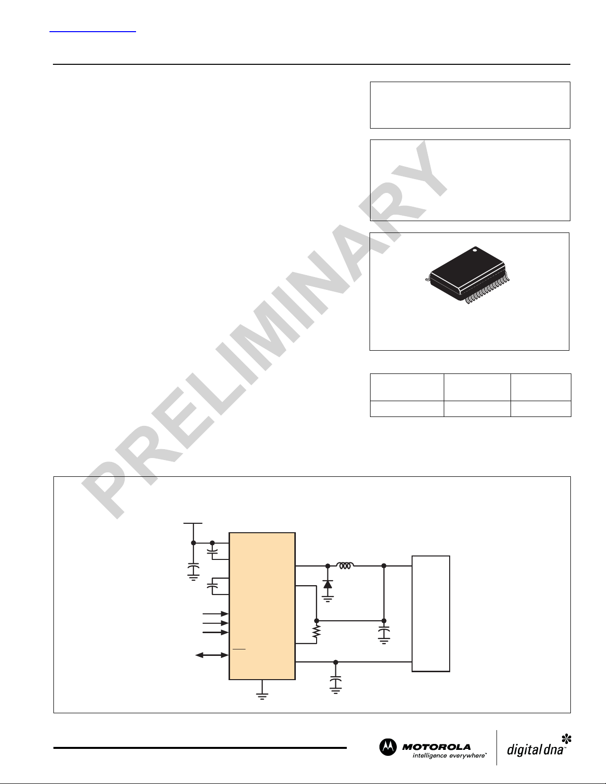
Adjustable Dual Output Switching
Power Supply
Document order number: MC34710
Rev 1.0, 04/2004
34710
The 34710 is a dual-output power regulator IC that integrates a switching
regulator, a linear regulator, supervisor circuitry, and a power supply
sequencer. With a wide operating input voltage range of 12 V to 32 V and
robust temperature limits, the 34710 is applicable in many commercial and
industrial applications that use an MCU.
A user-selectable 5.0 V/ 3.3 V buck switching regulator is provided for
board-level I/Os and user circuitry. The regulator is capable of delivering up to
1.0 A. The MCU core voltage is an adjustable 3.3 V / 2.5 V /1.8 V/1.5 V linear
voltage regulator that can supply up to 500 mA.
nc...
I
cale Semiconductor,
The switching and linear regulator output voltage are determined through
three digital input mode terminals that can be controlled by an MCU.
Features
• High-Current Adjustable 5.0 V/3.3 V Switching Regulator
• Low Noise User-Selectable 3.3 V/2.5 V/1.8 V / 1.5 V Linear Regulator
• On-Chip Thermal Shutdown and Error Reset Circuitry
• Supervisory Functions (Power-ON Reset and Error Reset Circuitry)
• Sequenced I/O and Core Voltages
• Pb-Free Packaging Designated by Suffix Code EW
Simplified Application Diagram
34710 Simplified Application Diagram
12 V to 32 V
34710
ADJUSTABLE DUAL OUTPUT
SWITCHING POWER SUPPLY
EW (Pb-FREE) SUFFIX
CASE 1324-02
32-LEAD SOICW-EP
ORDERING INFORMATION
Device
PC34710EW/R2 0°C to 85°C 32 SOICW-EP
Temperature
Range (T
)
A
Package
Frees
This document contains information on a product under development.
Motorola reserves the right to change or discontinue this product without notice.
© Motorola, Inc. 2004
B+
V
b
V
CP2
V
CP1
Mode0
Mode1
Mode2
RST
GND
For More Information On This Product,
Go to: www.freescale.com
SWITCH
I/O_OUT
LINB+
V
CORE
V
V
I/O
CORE
MCU
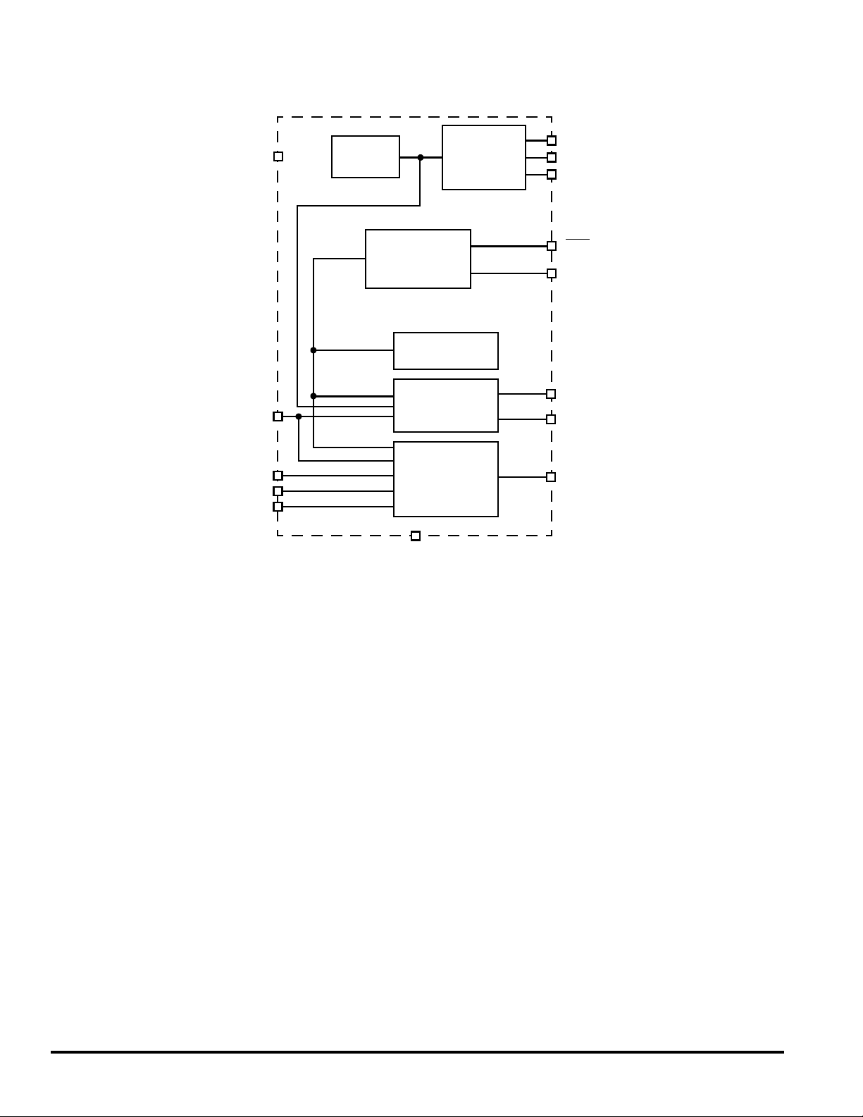
Freescale Semiconductor, Inc.
B+
nc...
I
MODE0
MODE1
MODE2
LINB+
Figure 1. 34710 Simplified Internal Block Diagram
2000 Hz
Oscillator
Supervisory and
Temperature
Shutdown
Switching
Regulator
Regulator
GND
Bandgap
V
I/O
V
CORE
Linear
Charge
Pump
cale Semiconductor,
CP1
CP2
V
b
RST
C
t
V
I/O_OUT
V
SWITCH
V
CORE
(2)
Frees
34710 MOTOROLA ANALOG INTEGRATED CIRCUIT DEVICE DATA
2
For More Information On This Product,
Go to: www.freescale.com
Freescale Semiconductor, Inc.
nc...
I
cale Semiconductor,
Frees
RST
MODE0
MODE1
MODE2
GND
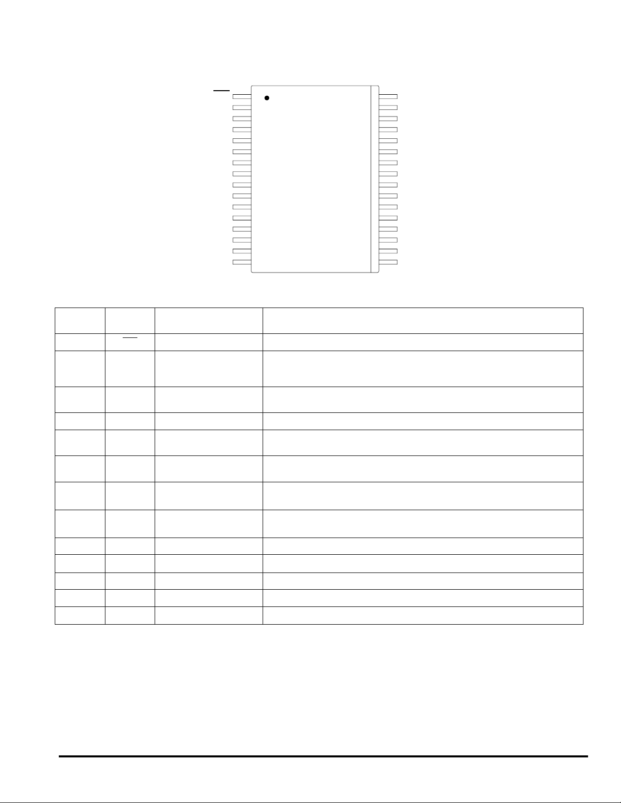
TERMINAL FUNCTION DESCRIPTION
Terminal
1
2
3
4
5– 12,
14–22
13 GND Ground
23, 24 V
25 LINB+ Core Voltage Regulator
26 V
27 V
28 B+ Power Supply Input
29 V
30 CP2 Switching Capacitor 2
31 CP1 Switching Capacitor 1
32 C
Terminal
Name
RST
MODE0
MODE1
MODE2
NC No Connects
CORE
I/O_OUT
SWITCH
b
t
Formal Name Definition
Reset
Mode Control These input terminals control V
Core Voltage Regulator
V
V
Output
Input
Switching Regulator
I/O
Feedback
Switching Regulator
I/O
Switch Output
Boost Voltage
Reset Delay Capacitor
NC
NC
NC
NC
NC
NC
NC
NC
NC
NC
NC
1
2
3
4
5
6
7
8
9
10
11
12
13
14
15
16
Reset input and output. This terminal is open drain.
No internal connection to this terminal.
Ground.
Core regulator output voltage.
Core regulator input voltage.
Feedback terminal for V
V
switching regulator switching output.
I/O
Regulator input voltage.
Boost voltage storage node.
Charge pump capacitor connection 2.
Charge pump capacitor connection 1.
Reset delay adjustment capacitor.
32
31
30
29
28
27
26
25
24
23
22
21
20
19
18
17
switching regulator and internal logic supply.
I/O
C
CP1
CP2
V
B+
V
V
LINB+
V
V
NC
NC
NC
NC
NC
NC
I/O_OUT
t
b
SWITCH
I/O_OUT
CORE
CORE
and V
output voltages.
CORE
MOTOROLA ANALOG INTEGRATED CIRCUIT DEVICE DATA 34710
For More Information On This Product,
Go to: www.freescale.com
3
Freescale Semiconductor, Inc.
MAXIMUM RATINGS
All voltages are with respect to ground unless otherwise noted.
Rating Symbol Max Unit
GLOBAL ABSOLUTE MAXIMUM RATINGS
Input Power Supply Voltage
I
= 0 A
B
+
Terminal Soldering Temperature (Note 1)
Power Dissipation (Note 2)
ESD Standoff Voltage
Non-Operating, Unbiased, Human Body Model (Note 3)
Thermal Resistance
Junction-to-Ambient (Note 4)
Junction-to-Ambient (Note 2)
Junction-to-Case
nc...
I
GLOBAL OPERATING RATINGS
Operating Ambient Temperature
Operating Device Junction Temperature
Input Power Supply Voltage
I
= 0 A to 3.0 A
B
+
Quiescent Bias Current from B+ (Note 5)
V
= 12 V to 32 V
B
+
Operating Junction Temperature
V
SWITCHING REGULATOR (Note 6)
I/O
Maximum Output Voltage Startup Overshoot (C
MODE0 = 0
MODE0 = Open
Maximum Output Current
cale Semiconductor,
T
= 0°C to 105°C
A
Notes
1. Soldering temperature limit is for 10 seconds maximum duration. Not designed for immersion soldering. Exceeding these limits may cause
malfunction or permanent damage to the device.
Frees
2. With 2.0 in
3. ESD1 testing is performed in accordance with the Human Body Model (C
4. With no additional heatsinking.
5. Maximum quiescent power dissipation is 0.25 W.
6. 12 V ≤ V
2
of copper headsink.
≤ 32 V and -20°C ≤ TJ ≤ 145°C unless otherwise noted.
B+
= 330 µF)
OUT
T
SOLDER
V
V
(STARTUP)
I/O
ZAP
V
B
+
P
D
ESD1
R
JA
θ
R
JA
θ
R
JC
θ
T
A
T
J
V
B
+
IB+(q)
T
J
I
VI/O
= 100 pF, R
ZAP
-0.3 to 36
260 °C
3.0 W
±2000
45
25
2.0
0 to 85 °C
105 °C
12 to 32
7.5
-0 to 105 °C
5.4
3.6
1.2
= 1500 Ω).
V
V
°C/W
V
mA
V
A
34710 MOTOROLA ANALOG INTEGRATED CIRCUIT DEVICE DATA
4
For More Information On This Product,
Go to: www.freescale.com
Freescale Semiconductor, Inc.
MAXIMUM RATINGS (continued)
All voltages are with respect to ground unless otherwise noted.
Rating Symbol Max Unit
V
LINEAR REGULATOR (Note 7)
CORE
Maximum Output Voltage Startup Overshoot (C
MODE[2:0] = [0,x,0]
MODE[2:0] = [0,x,Open]
MODE[2:0] = [Open,x,0]
MODE[2:0] = [Open,x,Open]
Maximum Output Current
T
= 0°C to 105°C, V
J
Notes
7. 12 V ≤ V
8. Refer to Table 1, page 10.
nc...
I
9. Pulse testing with low duty cycle used.
≤ 32 V and -20°C ≤ TJ ≤ 145°C unless otherwise noted.
B+
LINB
+
≤ V
(NOM) + 0.8 V (Note 9)
CORE
=10µF) (Note 8)
OUT
V
CORE
(STARTUP)
I
VCORE
V
3.6
2.7
2.0
1.65
mA
500
cale Semiconductor,
Frees
MOTOROLA ANALOG INTEGRATED CIRCUIT DEVICE DATA 34710
For More Information On This Product,
Go to: www.freescale.com
5

Freescale Semiconductor, Inc.
STATIC ELECTRICAL CHARACTERISTICS
Characteristics noted under conditions 4.75 V
≤ V
≤ 5.25 V, 12 V ≤ V
IO
≤ 32 V, and 0°C ≤ TJ ≤ 105°C unless otherwise noted.
B
+
Typical values noted reflect the approximate parameter mean at TA = 25°C under nominal conditions unless otherwise noted.
Characteristic Symbol Min Typ Max Unit
V
SWITCHING REGULATOR
I/O
V
I
LIMIT
V
VSWITCH
V
I
VCORE
V
I/O
I
VI/O
R
DS(ON)
(SOFT)
I/O
I
(OP)
LIMIT
(SOFT)
(NOM)
CORE
I
VCORE
(DROPOUT)
V
LINB
I
LIMIT
(MIN)
+
4.8
3.15
0.025 – 1.0
0.5 TBD 2.0
––2.5
2.1
1.3
-0.5 – –
3.15
2.35
1.71
1.425
1.0 – 500
0.8 – –
V
(NOM)
CORE
+ 1.0
800 – 1000
–
–
–
–
–
–
–
–
–
5.2
3.45
3.2
1.8
3.45
2.65
1.89
1.575
10
Logic Supply Voltage (I
MODE0 = 0
MODE0 = Open
Logic Supply Current
V
= Nominal, Power Dissipation in Switching Regulator = 0.45 W
I/O
Output On Resistance
V
= 12 V to 32 V
B
+
Soft Start Threshold Voltage
nc...
MODE0 = X
I
Current Limit Threshold (TJ = 25°C to 100°C)
Normal Operation
Soft Start, V
Minimum Voltage Allowable on V
= 25°C to 100°C
T
J
V
CORE
Supply Voltage (I
MODE[2:0] = [0,x,0]
MODE[2:0] = [0,x,Open]
MODE[2:0] = [Open,x,0]
MODE[2:0] = [Open,x,Open]
Supply Current
V
CORE
cale Semiconductor,
V
CORE
V
CORE
Regulator Input Voltage
V
Frees
CORE
Normal Current Limit Threshold
T
= 25°C to 100°C, V
J
Notes
10. Refer to Table 1
I/O
LINEAR REGULATOR
VCORE
= V
CORE
Dropout Voltage
= V
CORE
= V
CORE
= 25 mA to 1.0 A)
VI/O
≤ 2.5 V
SWITCH
= 5.0 mA to 500 mA) (Note 10)
(NOM)
(NOM), I
VCORE
(NOM), I
VCORE
= V
LINB
+
, page 10.
Terminal
= 0.5 A
= 0.5 A
(NOM) + 1.0 V
CORE
V
A
Ω
V
A
V
V
mA
V
V
mA
34710 MOTOROLA ANALOG INTEGRATED CIRCUIT DEVICE DATA
6
For More Information On This Product,
Go to: www.freescale.com

nc...
I
cale Semiconductor,
Frees
Freescale Semiconductor, Inc.
STATIC ELECTRICAL CHARACTERISTICS (continued)
Characteristics noted under conditions 4.75 V ≤ VIO ≤ 5.25 V, 12 V ≤ V
≤ 32 V, and 0°C ≤ TJ ≤ 105°C unless otherwise noted.
B
+
Typical values noted reflect the approximate parameter mean at TA = 25°C under nominal conditions unless otherwise noted.
Characteristic Symbol Min Typ Max Unit
MODE TERMINALS OPERATING VOLTAGES
MODE Control Terminals Low Voltage
T
= 0°C to TBD°C, V
J
MODE Control Terminals High Voltage
T
= 0°C to TBD°C, V
J
MODE Control Terminals Voltage with Input Floating
T
= 0°C to TBD°C, V
J
= 0°C to TBD°C, V
T
J
= 12 V to 32 V
B
+
= 12 V to 32 V
B
+
= 12 V to 14 V
B
+
= 14 V to 32 V
B
+
VIL(MODEn)
VIH(MODEn)
V
(FLOAT)
MODE
––0.825
2.6 – –
7.0
8.0
–
–
13.2
12
SUPERVISOR CIRCUITRY
(MIN)9.0––V
Minimum Function V
Minimum V
RST Low Voltage
V
B
RST V
V
V
RST Hysteresis for V
RST V
V
V
RST Hysteresis for V
V
B
V
CORE
V
B
Thermal Shutdown Temperature
T
J
Overtemperature Hysteresis
for RST Assertion, V
B
+
= 2.0 V, I
+
Threshold
I/O
Rising
I/O
Falling
I/O
Threshold
CORE
Rising
CORE
Falling
CORE
=12Vto32V
+
- V
for V
I/O
= 12 V to 32 V
+
Rising
for Charge Pump and Oscillator Running
B
+
≤ 5.0 mA
RST
I/O
CORE
Shutdown
CORE
Rising
B
+
V
B
+
(ASSERT)2.0– –V
V
B+
V
OL
––0.4
V
(NOM)
V
I/O
t+
V
I/O
t
-
V
HYSVI/O
V
CORE
t+
V
CORE
t
-
V
HYS CORE
(SHUTDOWN)
V
CORE
TSD)
TJ(
T
(HYSTERESIS)20 – TBD°C
J
–
V
(NOM)
I/O
- 225 mV
10 – 100 mV
–
V
(NOM)
CORE
- 225 mV
10 – 100
––TBD
170 – –
–
–
–
–
I/O
- 80 mV
V
CORE
- 80 mV
–
(NOM)
–
Vb CHARGE PUMP
V
V
V
V
V
V
mV
V
°C
Boost Voltage (Note 11)
V
= 12 V to 32 V, Ivb=0.5mA
B
+
Notes
11. Bulk capacitor ESR ≤ 10 Ω.
MOTOROLA ANALOG INTEGRATED CIRCUIT DEVICE DATA 34710
For More Information On This Product,
V
b
V
+10 V – V
B
+
B
+
+12 V
V
Go to: www.freescale.com
7

Freescale Semiconductor, Inc.
DYNAMIC ELECTRICAL CHARACTERISTICS
Characteristics noted under conditions 4.75 V
Typical values noted reflect the approximate parameter mean at TA = 25°C under nominal conditions unless otherwise noted
Characteristic Symbol Min Typ Max Unit
V
SWITCHING REGULATOR
I/O
Duty Cycle
Switching Rise and Fall Time
Load Resistance = 100 Ω, V
Switching Rise and Fall Time
Load Resistance = 100 Ω, V
SUPERVISOR CIRCUITRY
RST Delay
C
= 0.1 µF
nc...
I
cale Semiconductor,
delay
RST Filter Time
V
= 9.0 V
B
+
RST Fall Time
C
= 100 pF, R
L
External Low (Note 12)
V
= 5.0 V
I/O
RST Recovery Time Before Next RST Input (Note 12)
V
= 5.0 V
I/O
INTERNAL OSCILLATOR
Charge Pump and V
= 9.0 V to 32 V
V
B
+
Notes
12. See Figure 2,
13. t
is an input.
slpl
= 4.7 kΩ, 90% to 10%
PULLUP
Switching Regulator Operating Frequency
I/O
RST Timing, page 9.
B
+
B
+
= 30 V
= 30 V
≤ V
≤ 5.25 V, 12 V ≤ V
IO
≤ 32 V, and 0°C ≤ TJ ≤ 105°C unless otherwise noted.
B
+
D 45 – 55 %
tr, t
f
25 – –
t
+ t
r
f
––50
t
delay
t
filter
t
f
t
slpl
(Note 13)
t
phsl
f
OP
48 – 82
1.0 – 6.0
– – 125
30 – –
– – 10
140 – 260
ns
ns
ms
µs
ns
ns
µs
kHz
Frees
34710 MOTOROLA ANALOG INTEGRATED CIRCUIT DEVICE DATA
8
For More Information On This Product,
Go to: www.freescale.com

Freescale Semiconductor, Inc.
Timing Diagram
External
RST
Input
V
IH
V
IL
t
snl
t
t
slpl
nc...
I
34710
RST
V
IH
t
delay
phsl
cale Semiconductor,
Frees
V
IL
Figure 2. RST Timing
MOTOROLA ANALOG INTEGRATED CIRCUIT DEVICE DATA 34710
For More Information On This Product,
Go to: www.freescale.com
9

Freescale Semiconductor, Inc.
SYSTEM/APPLICATION INFORMATION
INTRODUCTION
V
Switching Regulator
I/O
The V
the MODE digital input terminals. The 34710’s MODE[2:0]
select the output voltage (Table 1
MODE[2:0] = 0, 0, 0, then V
Open, Open, then V
the output voltage of both regulators.
The topology of the regulator is a bang-bang buck regulator
operating from the internal ~200 kHz oscillator.
V
CORE
The V
nc...
I
1.8 V, or 1.5 V output voltage at 500 mA. The input to the
V
CORE
regulator output. The minimum input voltage must be
O
V
CORE
switching regulator output voltage is determined by
I/O
). For example, if
= 5.0 V; if MODE[2:0] = Open,
I/O
= 3.3 V. The MODE0 terminal controls
I/O
Linear Regulator
linear regulator can produce a +3.3 V, 2.5 V,
CORE
regulator is a terminal that may be connected to the V
(NOM)+0.8V.
SUPERVISORY AND MISCELLANEOUS FUNCTIONS
Introduction
The supervisor circuitry provides control of the RST line, an
open drain signal, based on system operating conditions
monitored by the 34710. V
shutdown (TSD) detectors in various parts of the chip are
monitored for error conditions. Because other devices in the
system may trigger a reset, the
but the supervisor circuitry controls all reset timing, including
externally generated resets. Driving the
cale Semiconductor,
system to be held in the reset state. V
thermal shutdown have both positive- and negative-going
thresholds.
The supervisor circuitry also ensures that the power supplies
Frees
sequence properly. Specifically, that V
TBD V below V
clamped at 0.5 V, and that the V
suppressed during startup and shutdown to ensure that
V
- V
CORE
= TBD V.
I/O
. This means that V
CORE
I/O
, V
, VB+, and thermal
CORE
RST line itself is also monitored,
RST line low causes the
, V
I/O
I/O
CORE
regulator operation will be
CORE
, VB+, and
CORE
is never less than
- V
will be
I/O
Static Operating Specifications
The RST output is an I/O device with an open drain output
driver with a pullup and a CMOS digital input gate (Figure 3
This I/O structure allows wired OR connection to the MCU’s
RST I/O terminal, as well as allowing the MCU to initiate a reset
cycle by driving its RST terminal low. When responding to a
MCU request for a reset cycle, the 34710 must respond rapidly
enough to prevent a glitch. Figure 2
, page 9, shows the timing
).
The MODE[2:0] terminals select the output voltage as
depicted in Table 1
Table 1. V
MODE2 MODE1 MODE0
000 5.0 3.3
0 0 Open 3.3 2.5
0 Open 0 5.0 1.8
0
Open 0 0 5.0 2.5
Open 0 Open 3.3 2.5
I/
Open Open 0 5.0 1.5
Open Open Open 3.3 1.5
Open indicates terminal is not connected externally.
parameters for responding to an externally applied
The rise time may be relatively slow, depending on the load
capacitance, and the internal
reliably (no oscillations during the transition) under these
conditions, i.e., the
t
(MAX). Error conditions must be present for a minimum
phsl
time, t
conditions are cleared, RST is held low for an additional time of
t
delay
threshold for t
when system operating conditions are met. The trigger for the
t
delay
V
CORE
1.0 µsto6.0µs delay.
, before the 34710 responds to them. Once all error
filter
. If any monitored item falls below its negative-going
retriggerable one shot should be ([V
(LOW) + VB+(LOW) + TJ(TSD)] & t
To Internal
Gates
From
Internal
Reset
Circuits
.
and V
I/O
Output Voltage Selection
Open
, 1.0 µs to 6.0 µs, the t
filter
Figure 3.
Open 3.3 1.8
RST input can be inhibited for up to
RST Terminal Interface
(NOM) Regulator
CORE
V
I/O
(V)
RST input gate must operate
delay
filter
RST
will be restarted
(LOW) +
I/O
), where t
V
I/O
V
(NOM)
CORE
(V)
RST signal.
filter
R
PULLUP
≥ 4.7 kΩ
(Optional)
C
LOAD
(Optional)
is the
34710 MOTOROLA ANALOG INTEGRATED CIRCUIT DEVICE DATA
10
For More Information On This Product,
Go to: www.freescale.com

Freescale Semiconductor, Inc.
Vb Charge Pump
The high-side MOSFETs in the H-Bridge motor drivers and
voltage regulators switch require a gate voltage in excess of
V
which is provided by the Vb supply. The Vb regulator is a
B+,
charge pump, switching directly off the V
internal oscillator operating at 200 kHz.
Power Dissipation
The power budget is described in Table 2. The maximum
dissipation for this device is 1.0 W continuous.
Table 2. Power Budget
Functional Block Watt
nc...
I
Bias
Charge Pump
Switching Regulator
Linear Regulator
Total
supply, and uses an
B+
0.00
0.15
0.45
0.35
0.95
Internal Oscillator
The internal oscillator provides timing for the charge pump
and switching regulators.
APPLICATIONS
cale Semiconductor,
Frees
MOTOROLA ANALOG INTEGRATED CIRCUIT DEVICE DATA 34710
For More Information On This Product,
Go to: www.freescale.com
11

Freescale Semiconductor, Inc.
PACKAGE DIMENSIONS
EW (Pb-FREE) SUFFIX
32-LEAD SOICW-EXPOSED PAD
PLASTIC PACKAGE
CASE 1324-02
ISSUE A
10.3
7.6
7.4
1
PIN 1 ID
nc...
I
BB
16
5.15
2X 16 TIPS
0.3 A
B C
A
A
C
32
17
B
95
4
11.1
10.9
9
(0.29)
0.25
0.19
0.38
6
0.22
2.65
2.35
BASE METAL
(0.203)
PLATING
C
L
A
32X
30X
0.65
SEATING
PLANE
0.10
R0.08 MIN
cale Semiconductor,
0.13MCAMB
SECTION A-A
ROTATED 90 CLOCKWISE
°
8
NOTES:
1. ALL DIMENSIONS ARE IN MILLIMETERS.
2. DIMENSIONING AND TOLERANCING PER ASME
Y14.5M, 1994.
3. DATUMS B AND C TO BE DETERMINED AT THE PLANE
WHERE THE BOTTOM OF THE LEADS EXIT THE
PLASTIC BODY.
4. THIS DIMENSION DOES NOT INCLUDE MOLD FLASH,
PROTRUSION OR GATE BURRS. MOLD FLASH,
PROTRUSION OR GATE BURRS SHALL NOT EXC EED
0.15 MM PER SIDE. THIS DIMENSION IS DETERMINED
AT THE PLANE WHERE THE BOTTOM OF THE LEADS
EXIT THE PLASTIC BODY.
5. THIS DIMENSION DOES NOT INCLUDE INTERLEAD
FLASH OR PROTRUSIONS. INTERLEAD FLASH AND
PROTRUSIONS SHALL NOT EXCEED 0.25 MM PER
SIDE. THIS DIMENSION IS DETERMINED AT THE
PLANE WHERE THE BOTTOM OF THE LEADS EXIT THE
PLASTIC BODY.
6. THIS DIMENSION DOES NOT INCLUDE DAMBAR
PROTRUSION. ALLOWABLE DAMB AR PROTRUSION
SHALL NOT CAUSE THE LEAD WIDTH TO EXCEED 0.4
MM PER SIDE. DAMBAR CANNOT BE LOCATED ON
THE LOWER RADIUS OR THE FOOT. MINIMUM SPACE
BETWEEN PROTRUSION AND ADJACENT LEAD
SHALL NOT LESS THAN 0.07 MM.
7. EXACT SHAPE OF EACH CORNER IS OPTIONAL.
8. THESE DIMENSIONS APPLY TO THE FLAT SECTION
OF THE LEAD BETWEEN 0.10 MM AND 0.3 MM FROM
A
0.25
GAUGE PLANE
THE LEAD TIP.
9. THE PACKAGE TOP MAY BE SMALLER THAN THE
PACKAGE BOTTOM. THIS DIMENSION IS
DETERMINED AT THE OUTERMOST EXTREMES OF
THE PLASTIC BODY EXCLUSIVE OF MOLD FLASH, TIE
BAR BURRS, GATE BURRS AND INTER-LEAD FLASH,
BUT INCLUDING ANY MISMATCH BETWEEN THE TOP
AND BOTTOM OF THE PLASTIC BODY.
°
0
MIN
0.9
°
8
0
0.5
°
SECTION B-B
0.29
0.13
Frees
34710 MOTOROLA ANALOG INTEGRATED CIRCUIT DEVICE DATA
12
For More Information On This Product,
Go to: www.freescale.com

Freescale Semiconductor, Inc.
nc...
I
NOTES
cale Semiconductor,
Frees
MOTOROLA ANALOG INTEGRATED CIRCUIT DEVICE DATA 34710
For More Information On This Product,
Go to: www.freescale.com
13

Freescale Semiconductor, Inc.
nc...
I
NOTES
cale Semiconductor,
Frees
34710 MOTOROLA ANALOG INTEGRATED CIRCUIT DEVICE DATA
14
For More Information On This Product,
Go to: www.freescale.com

Freescale Semiconductor, Inc.
nc...
I
NOTES
cale Semiconductor,
Frees
MOTOROLA ANALOG INTEGRATED CIRCUIT DEVICE DATA 34710
For More Information On This Product,
Go to: www.freescale.com
15

Freescale Semiconductor, Inc.
nc...
I
cale Semiconductor,
Frees
Information in this document is provided solely to enable system and software implementers to use Motorola products. There are no express or implied
copyright licenses granted hereunder to design or fabricate any integrated circuits or integrated circuits based on the information in this document.
Motorola reserves the right to make changes without further notice to any products herein. Motorola makes no warranty, representation or guarantee
regarding the suitability of its products for any particular purpose, nor does Motorola assume any liability arising out of the application or use of any product
or circuit, and specifically disclaims any and all liability, including without limitation consequential or incidental damages. “Typical” parameters which may be
provided in Motorola data sheets and/or specifications can and do vary in different applications and actual performance may vary over time. All operating
parameters, including “Typicals” must be validated for each customer application by customer’s technical experts. Motorola does not convey any license
under its patent rights nor the rights of others. Motorola products are not designed, intended, or authorized for use as components in systems intended for
surgical implant into the body, or other applications intended to support or sustain life, or for any other application in which the failure of the Motorola product
could create a situation where personal injury or death may occur. Should Buyer purchase or use Motorola products for any such unintended or
unauthorized application, Buyer shall indemnify and hold Motorola and its officers, employees, subsidiaries, affiliates, and distributors harmless against all
claims, costs, damages, and expenses, and reasonable attorney fees arising out of, directly or indirectly, any claim of personal injury or death associated
with such unintended or unauthorized use, even if such claim alleges that Motorola was negligent regarding the design or manufacture of the part.
MOTOROLA and the Stylized M Logo are registered in the US Patent and Trademark Office. All other product or service names are the property of their
respective owners.
© Motorola, Inc. 2004
HOW TO REACH US:
USA/EUROPE/LOCATIONS NOT LISTED: JAPAN: Motorola Japan Ltd.; SPS, Technical Information Center
Motorola Literature Distribution 3-20-1 Minami-Azabu. Minato-ku, Tokyo 106-8573, Japan
P.O. Box 5405, Denver, Colorado 80217 81-3-3440-3569
1-800-521-6274 or 480-768-2130
ASIA/PACIFIC: Motorola Semiconductors H.K. Ltd.; Silicon Harbour Centre
2 Dai King Street, Tai Po Industrial Estate, Tai Po, N.T., Hong Kong
852-26668334
HOME PAGE: http://motorola.com/semiconductors
For More Information On This Product,
Go to: www.freescale.com
MC34710
 Loading...