


查询33981供应商
Freescale Semiconductor, Inc.
MOTOROLA
SEMICONDUCTOR TECHNICAL DATA
Preliminary Information
High-Frequency, High-Current,
Self-Protected High-Side Switch
Document order number: MC33981
Rev 2.0, 10/2004
33981
(4.0 mΩ up to 60 kHz)
The 33981 is a high-frequency, self-protected 4.0 mΩ R
switch used to replace electromechanical relays, fuses, and discrete devices
in power management applications.
The 33981 can be controlled by pulse-width modulation (PWM) with a
frequency up to 60 kHz. It is designed for harsh environments, and it includes
self-recovery features. The 33981 is suitable for loads with high inrush current,
as well as motors and all types of resistive and inductive loads.
nc...
, I
or
emiconduct
The 33981 is packaged in a 12 x 12 nonleaded power-enhanced Power
QFN package with exposed tabs.
Features
• Single 4.0 mΩ R
• PWM Capability up to 60 kHz with Duty Cycle from 5% to 100%
• Very Low Standby Current
• Slew Rate Control with External Capacitor
• Overcurrent and Overtemperature Protection, Undervoltage Shutdown
and Fault Reporting
• Reverse Battery Protection
• Gate Drive Signal for External Low-Side N-Channel MOSFET with
Protection Features
• Output Current Monitoring
• Temperature Feedback
Maximum High-Side Switch
DS(ON)
33981 Simplified Application Diagram
DS(ON)
high-side
Device
PC33981PNA/R2
Simplified Application Diagram
HIGH-SIDE SWITCH
4.0 mΩ
Bottom View
PNA SUFFIX
SCALE 1:1
CASE 1402-02
16-TERMINAL PQFN (12 X 12)
ORDERING INFORMATION
Temperature
Range (T
-40°C to 125°C
)
A
Package
16 PQFN
V
DD
V
eescale S
Fr
I/O
I/O
I/O
MCU
I/O
A/D
A/D
This document contains information on a product under development.
Motorola reserves the right to change or discontinue this product without notice.
© Motorola, Inc. 2004
For More Information On This Product,
Go to: www.freescale.com
DD
SR
CONF
FS
INLS
EN
INHS
TEMP
CSNS
33981
V
C
V
PWR
PWR
BOOT
OUT
DLS
GLS
GNDOCLS
M

TEMP
Temperature
Feedback
Freescale Semiconductor, Inc.
Undervoltage
Detection
Bootstrap Supply
V
PWR
C
BOOT
nc...
, I
or
emiconduct
SR
FS
EN
INHS
INLS
CONF
5.0 V
I
CONF
R
DWN
Slew Rate Control
Logic
I
DWN
Cross-
Conduction
Figure 1. 33981 Simplified Internal Block Diagram
Current Protection
100 A
Overtemperature
Detection
GND
Gate Driver
OUT Current
Recopy
1/20000
5.0 V
CSNS
Low-Side
Gate Driver
and Protection
I
OCLS
OCLS
OUT
GLS
DLS
eescale S
Fr
33981 MOTOROLA ANALOG INTEGRATED CIRCUIT DEVICE DATA
2
For More Information On This Product,
Go to: www.freescale.com

Transparent Top View of Package
Freescale Semiconductor, Inc.
nc...
, I
or
emiconduct
CSNS
TEMP
EN
INHS
FS
INLS
CONF
OCLS
DLS
GLS
SR
C
BOOT
TERMINAL DEFINITIONS
Functional descriptions of some of these terminals can be found in the System /Application Information section beginning on
page 19
.
Terminal
1 CSNS Output Current Monitoring This terminal is used to output a current proportional to the high-side OUT current and
2 TEMP Temperature Feedback This terminal reports an analog value proportional to the temperature of the GND flag
3
4 INHS Serial Input High Side The input terminal is used to directly control the OUT. This input has an active internal
5
6 INLS Serial Input Low Side The input terminal is used to directly control an external low-side N-channel MOSFET
Terminal
Name
EN
FS
Formal Name Definition
Enable
(Active High)
Fault Status
(Active Low)
1
2
3
4
5
13
6
GND
7
8
9
10
11
12
is used externally to generate a ground-referenced voltage for the microcontroller
(MCU) to monitor OUT current.
(terminal 13). It is used by the MCU to monitor board temperature.
This is an input used to place the device in a low current sleep mode. This terminal has
an passive internal pulldown.
pulldown current source and requires CMOS logic levels.
This is an open drain-configured output requiring an external pull-up resistor to
V
(5.0 V) for fault reporting. When a device fault condition is detected, this terminal
DD
is active LOW.
and has an active internal pulldown current source and requires CMOS logic levels. It
can be controlled independently of the INHS depending of CONF terminal.
V
14
PWR
16
15
OUT
OUT
eescale S
Fr
7 CONF Configuration Input This input terminal is used to manage the cross-conduction between the internal high-
8 OCLS Low-Side Overload This terminal sets the V
9 DLS Drain Low Side This terminal is the drain of the external low-side N-channel MOSFET. Its monitoring
10 GLS Low-Side Gate This terminal is an output used to drive the gate of the external low-side N-channel
11 SR Slew Rate Control A capacitor connected between this terminal and the ground is used to control the
MOTOROLA ANALOG INTEGRATED CIRCUIT DEVICE DATA 33981
side N-channel MOSFET and the external low-side N-channel MOSFET. The terminal
has an active internal pullup current source. When CONF is at 0 V, the two MOSFETs
are controlled independently. When CONF is at 5.0 V, the two MOSFETs cannot be on
at the same time.
protection level of the external low-side MOSFET. This
terminal has an active internal pullup current source. It must be connected to an
external resistor.
allows for protection features.
MOSFET.
output slew rate.
DS
For More Information On This Product,
Go to: www.freescale.com
3

Freescale Semiconductor, Inc.
TERMINAL DEFINITIONS (continued)
Functional descriptions of some of these terminals can be found in the System /Application Information section beginning on
page 19
.
Terminal
14 V
15, 16 OUT Output Protected high-side power output to the load. Output terminals must be connected in
Terminal
Name
PWR
Formal Name Definition
Positive Power Supply This terminal connects to the positive power supply and is the source input of
operational power for the device. The V
of the package.
parallel for operation.
terminal is a backside surface mount tab
PWR
nc...
, I
or
emiconduct
eescale S
Fr
33981 MOTOROLA ANALOG INTEGRATED CIRCUIT DEVICE DATA
4
For More Information On This Product,
Go to: www.freescale.com

Freescale Semiconductor, Inc.
MAXIMUM RATINGS
All voltages are with respect to ground unless otherwise noted.
Rating Symbol Value Unit
ELECTRICAL RATINGS
Power Supply Voltage
Steady-State
V
PWR
V
-16 to 41
nc...
, I
or
emiconduct
eescale S
Fr
Input/Output Terminals Voltage (Note 1) V
Output Voltage V
Continuous Output Current (Note 2) I
CSNS Input Clamp Current I
SR Voltage V
Temperature Feedback Voltage V
Voltage
C
BOOT
OCLS Voltage V
Low-Side Gate Voltage V
Low-Side Drain Voltage V
ESD Voltage
Human Body Model (Note 3)
Machine Model (Note 4)
Output Clamp Energy (Note 5) E
CSNS
C
BOOT
OCLS
V
ESD1
V
ESD2
IN
OUT
OUT
SR
TEMP
GLS
DLS
CL
-0.3 to 7.0 V
-5.0 to 41 V
40 A
10 mA
-0.3 to 54 V
-0.3 to 5.0 V
-0.3 to 54 V
-0.3 to 7.0 V
-0.3 to 15 V
-5.0 to 41 V
±2000
±200
TBD J
THERMAL RATINGS
Operating Temperature
Ambient
Junction
Storage Temperature T
Thermal Resistance (Note 6)
Junction to Power Die Case
Junction to Ambient
Peak Terminal Reflow Temperature During Solder Mounting (Note 7) T
Power Dissipation (TA = 25°C) (Note 8) P
Notes
1. Exceeding voltage limits on INHS, INLS, CONF, CSNS,
device.
2. Continuous high-side output rating as long as maximum junction temperature is not exceeded. Calculation of maximum output current using
package thermal resistance is required.
3. ESD1 testing is performed in accordance with the Human Body Model (C
4. ESD2 testing is performed in accordance with the Machine Model (C
specification with a capacitor > 0.01 µF connected from OUT to GND.
5. Active clamp energy using single-pulse method (L = 16 mH, R
6. Device mounted on a 2s2p test board per JEDEC JESD51-2.
7. Terminal soldering temperature limit is for 10 seconds maximum duration. Not designed for immersion soldering. Exceeding these limits may
cause malfunction or permanent damage to the device.
8. Maximum power dissipation at indicated ambient temperature in free air with no heatsink used.
FS, TEMP, and EN terminals may cause a malfunction or permanent damage to the
ZAP
= 0, V
PWR
L
T
A
T
J
STG
R
JC
θ
R
JA
θ
SOLDER
D
= 100 pF, R
ZAP
= 200 pF, R
= 12 V, TJ = 150°C).
= 0 Ω) and in accordance with the system module
ZAP
= 1500 Ω).
ZAP
-40 to 125
-40 to 150
-55 to 150
°C/W
1.0
20
240 °C
TBD W
°C
°C
V
MOTOROLA ANALOG INTEGRATED CIRCUIT DEVICE DATA 33981
For More Information On This Product,
Go to: www.freescale.com
5

Freescale Semiconductor, Inc.
STATIC ELECTRICAL CHARACTERISTICS
Characteristics noted under conditions 4.5 V ≤ VDD≤ 5.5 V, 6.0 V ≤ V
≤ 27 V, -40°C ≤ TJ≤ 150°C unless otherwise noted.
PWR
Typical values noted reflect the approximate parameter mean at TA = 25°C under nominal conditions unless otherwise noted.
Characteristic Symbol Min Typ Max Unit
POWER INPUT
Battery Supply Voltage Range
Fully Operational
Extended
V
PWR
6.0
4.5
–
–
27
27
V
Supply Current
V
PWR
Output ON, I
Supply Current
V
PWR
Output OFF, EN = 5.0 V, OUT Connected to GND
Sleep State Supply Current (V
T
= 25°C
nc...
, I
or
J
= 125°C
T
J
Undervoltage Shutdown V
Undervoltage Hysteresis V
OUT
= 0 A
< 14 V, EN = 0V)
PWR
POWER OUTPUT
Output Drain-to-Source ON Resistance (I
= 6.0 V
V
PWR
= 10.0 V
V
PWR
= 13 V
V
PWR
Output Drain-to-Source ON Resistance (I
emiconduct
Output Drain-to-Source ON Resistance
V
V
V
V
PWR
PWR
PWR
PWR
= 6.0 V
= 9.0 V
= 13 V
= - 13 V
= 20 A, TJ = 25°C)
OUT
= 20 A, TJ = 150°C)
OUT
(I
= 20 A, TJ = 25°C)
OUT
I
PWR(ON)
I
PWR(SBY)
I
PWR(SLEEP)
PWR(UV)
PWR(UVHYS)
R
DS(ON)
R
DS(ON)
R
DS(ON)
mA
––10
mA
––10
µA
–
–
2.0 – 4.0 V
–0.3–V
–
–
–
–
–
–
––8.0
–
–
–
–
–
–
–
–
5.0
50
mΩ
6.0
5.0
4.0
mΩ
10.2
8.5
6.8
mΩ
Output Overcurrent Detection Level I
eescale S
Current Sense Ratio
Fr
9.0 V <
V
< 16 V, CNS < 4.5V
PWR
Current Sense Ratio (C
Output Current
5.0 A
10 A
30 A
Current Sense Voltage Clamp
I
= 15 mA
CCNS
33981 MOTOROLA ANALOG INTEGRATED CIRCUIT DEVICE DATA
6
) Accuracy
SR
For More Information On This Product,
OCH
C
SR
C
SR_ACC
V
CL(CSNS)
– – 100 A
– 1/20000 –
-20
-14
-12
4.5 6.0 7.0
–
–
–
20
14
12
Go to: www.freescale.com
–
%
V

Freescale Semiconductor, Inc.
STATIC ELECTRICAL CHARACTERISTICS (continued)
Characteristics noted under conditions 4.5 V ≤ V
≤ 5.5V, 6.0V≤ V
DD
Typical values noted reflect the approximate parameter mean at T
Characteristic Symbol Min Typ Max Unit
A
≤ 27 V, -40°C ≤ TJ≤ 150°C unless otherwise noted.
PWR
= 25°C under nominal conditions unless otherwise noted.
POWER OUTPUT (continued)
Overtemperature Shutdown T
Overtemperature Shutdown Hysteresis (Note 9) T
Low-Side Gate
V
= 6.0 V
PWR
= 9.0 V
V
PWR
= 13 V
V
PWR
= 27 V
V
PWR
SD
SD(HYS)
V
GSLS
160 175 190 °C
5.0 – 20
–
–
–
–
6.0
9.0
12
12
°C
V
–
–
–
–
nc...
, I
or
emiconduct
eescale S
Fr
Low-Side Gate Current
C = 4.7 nF
Low-Side Overload Detection Level versus Low-Side Drain Voltage
V
- V
OCLS
DLS
Temperature Feedback
= 25°C
T
J
Temperature Feedback Derating DT
I
GSLS
V
DS_LS
T
Feed
Feed
CONTROL INTERFACE
Input Logic High Voltage (Note 10) V
Input Logic Low Voltage (Note 10) V
Input Logic Voltage Hysteresis (Note 10) V
Input Logic Active Pulldown Current (INHS, INLS) I
Input Logic Pulldown Resistor (EN)
Input Active Pullup Current (OCLS)
Input Active Pullup Current (CONF) I
FS Tri-State Capacitance (Note 9)
FS Low-State Output Voltage
Notes
9. Parameter is guaranteed by process monitoring but is not production tested.
10. Upper and lower logic threshold voltage range applies to EN, CONF, INHS, and INLS input signals.
IH
IL
IN(HYS)
DWN
R
DWN
I
OCLS
CONF
C
SO
V
SOL
p
mA
–100–
mV
––50
V
TBD 4.75 TBD
–-12–mV/°C
0.7 – – V
– – 0.2 V
100 350 750 mV
5.0 – 20 µA
100 200 400 kΩ
–100–µA
–10–µA
– – 20 pF
–0.20.4V
DD
DD
MOTOROLA ANALOG INTEGRATED CIRCUIT DEVICE DATA 33981
For More Information On This Product,
Go to: www.freescale.com
7

Freescale Semiconductor, Inc.
DYNAMIC ELECTRICAL CHARACTERISTICS
Characteristics noted under conditions 4.5 V ≤ VDD≤ 5.5 V, 6.0 V ≤ V
Typical values noted reflect the approximate parameter mean at TA = 25°C under nominal conditions unless otherwise noted.
Characteristic Symbol Min Typ Max Unit
CONTROL INTERFACE AND POWER OUTPUT TIMING
C
Charge Blanking Time (Note 11)
BOOT
≤ 27 V, -40°C ≤ TJ≤ 150°C unless otherwise noted.
PWR
t
ON
– 20 – µs
Output Rising Slew Rate (Note 12)
V
= 14 V
PWR
= 6.8 nF, from 10% to 90% of V
C
GATE
Output Falling Slew Rate (Note 12)
V
= 14 V
PWR
= 6.8 nF, from 90% to 10% of V
C
GATE
Output Turn-ON Delay Time (Note 13)
nc...
Output Turn-OFF Delay Time
Input Switching Frequency (Note 14) f
, I
Notes
or
11. Refer to the paragraph entitled Sleep Mode
12. Parameter is guaranteed by process monitoring but is not production tested.
13. Turn-ON delay time measured from rising edge of INHS that turns the output ON to V
14. Turn-OFF delay time measured from falling edge of INHS that turns the output OFF to V
SR Capacitor = 4.7 nF
OUT,
SR Capacitor = 4.7 nF
OUT,
on page 19.
SR
SR
t
DLY(ON)
t
DLY(OFF)
PWM
emiconduct
R
–
–
F
–
–
– 200 – ns
– 400 – ns
– – 60 kHz
= 0.5 V with RL= 5.0 Ω resistive load.
OUT
= V
OUT
PWR
25
–
25
–
-0.5 V with RL= 5.0 Ω resistive load.
–
–
–
–
V/µs
V/µs
eescale S
Fr
33981 MOTOROLA ANALOG INTEGRATED CIRCUIT DEVICE DATA
8
For More Information On This Product,
Go to: www.freescale.com

nc...
, I
or
Freescale Semiconductor, Inc.
Condition CONF INHS INLS OUT GLS
Sleep x x x x x H L Device is in Sleep mode. The OUT and
Normal L H H H H H H Normal mode. High side and low side are
Normal L L L L L H H Normal mode. High side and low side are
Normal H L H L H H H Normal mode. No cross-conduction. Half-
Normal H H L H L H H Normal mode. No cross-conduction. Half-
Normal H PWM H PWM PWM
H = High level
L = Low level
x = Don’t care
PWM = Pulse-width modulation
Table 1. Functional Truth Table in Normal Mode
FS
EN Comments
low-side gate are OFF.
controlled independently. The high side
and the low side are both on.
controlled independently. The high side
and the low side are both off.
bridge configuration. The high side is off
and the low side is on.
bridge configuration. The high side is on
and the low side is off.
OR H
(Logical
OR)
H H Normal mode. Cross-conduction
management is activated. Half-bridge
configuration.
emiconduct
eescale S
Fr
Table 2. Functional Truth Table in Fault Mode
Conditions CONF INHS INLS OUT GLS
Overtemperature
on OUT
Overtemperature
on C
on External Low-
Side MOSFET
H = High level
L = Low level
x = Don’t care
or GLS
BOOT
Overcurrent
on OUT
Overload
x x x L x L H L x x The 33981 is currently in fault mode. The
x x x L L L H L x x The 33981 is currently in fault mode. The
x H x L x L H x L x The 33981 is currently in fault mode. The
L x H x L L H x x L The 33981 is currently in fault mode. GLS
FS
EN TEMP CSNS OCLS Comments
OUT is OFF. TEMP at 0 V indicates this
fault. Once the fault is removed 33981
recovers its normal mode.
OUT is OFF and GLS is at 0 V. TEMP at
0 V indicates this fault. Once the fault is
removed 33981 recovers its normal mode.
OUT is OFF. It is reset by a logic [0] at
INHS for at least 200 µs. When INHS goes
to 0 V, CSNS goes to 5.0 V.
is at 0 V and OCLS internal current source
is off. The external resistance connected
between OCLS and GND terminal will pull
OCLS terminal to 0 V. The fault is reset by
a logic [0] at INLS for at least 200 µs.
MOTOROLA ANALOG INTEGRATED CIRCUIT DEVICE DATA 33981
For More Information On This Product,
Go to: www.freescale.com
9

V
PWR
- 0.5 V
Freescale Semiconductor, Inc.
Timing Diagram
INHS
nc...
, I
or
emiconduct
0.5 V
OUT
t
DLY(ON)
Figure 2. Time Delays
t
DLY(OFF)
eescale S
Fr
33981 MOTOROLA ANALOG INTEGRATED CIRCUIT DEVICE DATA
10
For More Information On This Product,
Go to: www.freescale.com

Freescale Semiconductor, Inc.
Functional Diagrams
EN
nc...
, I
or
emiconduct
CONF
INHS
INLS
OUT
GLS
FS
TEMP
Temperature
OUT
High Side ON
Low Side ON
Thermal Shutdown on OUT
0V
Thermal Shutdown on OUT
5.0 V
0V
Thermal Shutdown
on OUT
0V
Thermal Shutdown on OUT
TSD
Figure 3. Overtemperature on Output
High Side ON
Hysteresis
High Side OFF
Thermal Shutdown on OUT
0V
Thermal Shutdown
on OUT
Thermal Shutdown on OUT
TSD
High Side OFF
Hysteresis
5.0 V
0V
eescale S
Fr
MOTOROLA ANALOG INTEGRATED CIRCUIT DEVICE DATA 33981
For More Information On This Product,
Go to: www.freescale.com
11

EN
Freescale Semiconductor, Inc.
nc...
, I
or
emiconduct
CONF
INHS
INLS
OUT
GLS
FS
TEMP
Temperature
Control
Figure 4. Overtemperature on Bootstrap Circuit or on Low-Side Gate Drive
High Side ON
Thermal Shutdown
0V
Thermal Shutdown
0V
Thermal Shutdown
Thermal Shutdown
TSD
Hysteresis Hysteresis
High Side OFF
Low Side ON
on
Bootstrap Circuit or on Low-Side Gate Drive
Thermal Shutdown
0V
Thermal Shutdown
5.0 V
15 µs After 15 µs After
Thermal Shutdown
Thermal Shutdown
TSD
0V
0V
eescale S
Fr
33981 MOTOROLA ANALOG INTEGRATED CIRCUIT DEVICE DATA
12
For More Information On This Product,
Go to: www.freescale.com
Freescale Semiconductor, Inc.
EN
nc...
, I
or
emiconduct
eescale S
Fr
INLS
GLS
FS
OCLS
V
DS_LS
EN
INLS
GLS
0V
200 µs Min
Overload on Low Side
Low Side OFF
0V
Overload on Low Side
0V
Overload on Low Side
0V
Overload on Low Side
V
DS_LS = VOCLS
Case 1: Overload Removed
Figure 5. Overload on Low-Side Gate Drive, Case 1
0V
200 µs Min
Overload on Low Side
Low Side OFF
0V
Overload on Low Side
5.0 V
FS
OCLS
V
DS_LS
MOTOROLA ANALOG INTEGRATED CIRCUIT DEVICE DATA 33981
Overload on Low Side
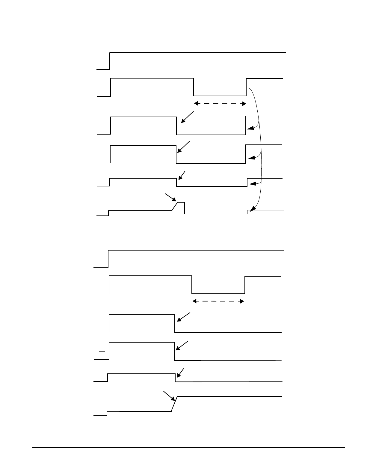
Figure 6. Overload on Low-Side Gate Drive, Case 2
V
DS_LS = VOCLS
For More Information On This Product,
0V
Overload on Low Side
0V
Case 2: Low Side Still Overloaded
13
Go to: www.freescale.com

EN
Freescale Semiconductor, Inc.
nc...
, I
or
emiconduct
INHS
OUT
FS
CSNS
I
OUT
EN
FS
Overcurrent on High Side
15 µs After
0V
200 µs Min
Overcurrent on High Side
0V
Overcurrent on High Side
0V
5.0 V
0V
Overcurrent on High Side
I
OCH
Figure 7. Overcurrent on Output
5.0 V
Fault Removed
5.0 V
CONF
eescale S
Fr
33981 MOTOROLA ANALOG INTEGRATED CIRCUIT DEVICE DATA
14
INHS
INLS
OUT
GLS
Figure 8. Normal Mode. Cross-Conduction Management
For More Information On This Product,
Go to: www.freescale.com

EN
FS
Freescale Semiconductor, Inc.
15 µs After
nc...
, I
or
emiconduct
CONF
INHS
INLS
OUT
GLS
High Side ON
Figure 9. Normal Mode. Independent High Side and Low Side
I
OUT
Iout
High Side OFF
INHS
INHS
0V
CS N S
CSNS
eescale S
Fr
FS
FS
Figure 10. High-Side Overcurrent
MOTOROLA ANALOG INTEGRATED CIRCUIT DEVICE DATA 33981
For More Information On This Product,
Go to: www.freescale.com
15

Freescale Semiconductor, Inc.
INHS
GLS
Iout
Recirculation in Low SideCurrent in Motor
OUT
nc...
, I
or
emiconduct
eescale S
Fr
Figure 11. Cross-Conduction with Low Side
Overtemperature
INHS
TEMP
OUT
I
OUT
Figure 12. Overtemperature on OUT
33981 MOTOROLA ANALOG INTEGRATED CIRCUIT DEVICE DATA
16
For More Information On This Product,
Go to: www.freescale.com

Freescale Semiconductor, Inc.
EN
nc...
, I
or
emiconduct
TEMP
Figure 13. Overtemperature on Bootstrap Circuit or on Low-Side Gate Drive
Overtemperature
OUT
I
OUT
eescale S
Fr
Figure 14. Maximum Operating Frequency for SR Capacitor of 4.7 nF
MOTOROLA ANALOG INTEGRATED CIRCUIT DEVICE DATA 33981
For More Information On This Product,
Go to: www.freescale.com
17

Freescale Semiconductor, Inc.
Electrical Performance Curves
7.0
6.0
5.0
4.0
(mΩ)
3.0
DS(ON)
2.0
R
RdsON (mOhm )
1.0
0.0
-50 0 50 100 150 200
Temperature (°C)
Temperature (°C)
nc...
, I
or
emiconduct
eescale S
Fr
(µA)
Ipwr(sleep)(µA)
I
PWR(SLEEP)
10.0
9.0
8.0
7.0
6.0
5.0
4.0
3.0
2.0
1.0
0.0
Figure 15. R
4.5 6.0 9.0 12.0 12.5 13.0 14.0 17.0 21.0
Figure 16. Sleep State Supply Current versus V
versus Temperature
DS(ON)
V
Vpwr(V)
PWR
(V)
PWR
at 150°C
33981 MOTOROLA ANALOG INTEGRATED CIRCUIT DEVICE DATA
18
For More Information On This Product,
Go to: www.freescale.com

Freescale Semiconductor, Inc.
SYSTEM/APPLICATION INFORMATION
INTRODUCTION
The 33981 is a high-frequency self-protected silicon 4.0 mΩ
R
relays, fuses, and discrete devices in power management
applications. The 33981 can be controlled by pulse-width
modulation (PWM) with a frequency up to 60 kHz. It is designed
for harsh environments, and it includes self-recovery features.
high-side switch used to replace electromechanical
DS(ON)
Sleep Mode
Sleep mode is the state of the 33981 when the EN is logic [0].
In this mode, OUT, the gate driver for the external MOSFET,
and all unused internal circuitry are off to minimize current draw.
nc...
, I
or
The 33981 will go to the normal operating mode when the EN
terminal is logic [1]. The INHS and INLS commands will be
disabled typically 20 µs after the EN transitions to logic [1] to
enable the charge of the bootstrap capacitor.
Fault Logic
This 33981 indicates the faults below as they occur by
driving the FS terminal to logic [0]:
• Overtemperature
• Overcurrent fault on OUT
• Overload fault on the external low-side MOSFET
The
emiconduct
FS terminal will return to logic [1] when the
overtemperature fault condition is removed. The two other
faults are latched.
Undervoltage
The latched faults are reset when the V
V
eescale S
Overtemperature Fault
Fr
shutdown circuitry on OUT. Overtemperature detection also
protects the bootstrap circuit (C
gate driver (GLS terminal). Overtemperature detection occurs
when OUT is in the ON or OFF state and GLS is at high or low
level.
turning OFF until the temperature falls below T
continue indefinitely until the offending load is removed.
low-side gate drive results in OUT turning OFF and the GLS
going to 0 V until the temperature falls below T
continue indefinitely until the offending load is removed.
.
PWR(UV)
The 33981 incorporates overtemperature detection and
terminal) and the low-side
BOOT
For OUT, an overtemperature fault condition results in OUT
Figure 12
An overtemperature fault on the bootstrap circuit or on the
, page 16, shows an overtemperature on OUT.
voltage is below
PWR
SD
SD
The 33981 is suitable for loads with high inrush current, as
well as motors and all types of resistive and inductive loads. A
dedicated parallel input is available for an external low-side
control with protection features and cross-conduction
management.
FUNCTIONAL DESCRIPTION
terminal transition to logic [1] will be disabled typically 15 µs
after to enable the charge of the bootstrap capacitor.
Figure 13
bootstrap circuit or on the low-side gate drive. As the
temperature increases, TEMP voltage decreases until thermal
shutdown.
Overtemperature faults force the TEMP terminal to 0 V.
Overcurrent Fault on High Side
The OUT terminal has a 100 A overcurrent high-detection
level for maximum device protection. If at any time the current
reaches this level, OUT will stay OFF and the CSNS terminal
will go to 0 V. The OUT terminal is reset by a logic [0] at the
INHS terminal for at least 200 µs. When INHS goes to 0 V,
CSNS goes to 5.0 V.
In Figure 11
0 V. When the current reaches I
10 µs owing to internal logic circuit.
Overload Fault on Low Side
This fault detection is active when INLS is logic [1]. Low-side
overload protection does not measure the current directly but
rather its effects on the low-side MOSFET. When V
. This cycle will
. This cycle will
FS
and V
0 V and the OCLS internal current source is disconnected and
OCLS goes to 0 V. The GLS terminal and the OCLS terminal
are reset by a logic [0] at the INLS terminal for at least 200 µs.
with its internal current source sets the V
the external resistance, the protection level can be adjusted
depending on low-side characteristics. A 3.3 kΩ resistor gives
a V
drain of the low side (DLS terminal) and the 33981 ground
(GND terminal). It also uses the voltage across the external
resistance connected to the OCLS terminal and the GND
terminal. For this reason it is key that the low-side source, the
33981 ground, and the external resistance ground connection
are connected together in order to prevent false error detection
due to ground shifts.
> V
DLS
When connected to an external resistor, the OCLS terminal
level of 3.3 V typical.
DSH
This protection circuitry measures the voltage between the
, page 17, shows an overtemperature on the
, page 16, the OUT terminal is short-circuited to
, OUT is turned OFF within
OCH
> V
GLS
for at least 2.5 µs, the GLS terminal goes to
DSH
level. By changing
DSH
GSH
MOTOROLA ANALOG INTEGRATED CIRCUIT DEVICE DATA 33981
For More Information On This Product,
19
Go to: www.freescale.com

Freescale Semiconductor, Inc.
Configuration
The CONF terminal manages the cross-conduction between
the internal MOSFET and the external low-side MOSFET. With
the CONF terminal at 0 V, the two MOSFETs can be
independently controlled. A load can be placed between the
high side and the low side.
With the CONF terminal at 5.0 V, the two MOSFETs cannot
be on at the same time. They are in half-bridge configuration as
shown in the simplified application diagram on page 1
and INLS are at 5.0 V at the same time, INHS has priority and
OUT will be at V
INLS at 5.0 V, GLS will go to high state as soon as the VGS of
the internal MOSFET is lower than TBD typically. A half-bridge
application could consist in sending PWM signal to the INHS
terminal and 5.0 V to the INLS terminal with the CONF terminal
at 5.0 V.
Figure 11
diagram on page 1
nc...
CONF and INLS terminals are at 5.0 V. When INHS is at 5.0 V,
current is flowing in the motor. When INHS goes to 0 V, the load
, I
current recirculates in the external low side.
, page 16, illustrates the simplified application
. If INHS changes from 5.0 V to 0 V with
PWR
with a DC motor and external low side. The
. If INHS
or
Bootstrap Supply
Bootstrap supply provides current to recharge the bootstrap
capacitor through the V
after the application of power to the device to charge the
bootstrap capacitor. A typical value for this capacitor is 100 nF.
An internal charge pump allows continuous MOSFET drive.
When the device is in the sleep mode, this bootstrap supply is
off to minimize current consumption.
terminal. A short time is required
PWR
emiconduct
High-Side Gate Driver
The high-side gate driver switches the bootstrap capacitor
voltage to the gate of the MOSFET. The driver circuit has a lowimpedance drive to ensure that the MOSFET remains OFF in
the presence of fast falling dV/dt transients on the OUT
terminal.
This bootstrap capacitor connected between the power
eescale S
supply and the C
to drive the device. The voltage across this capacitor is limited
Fr
to about 13 V. C
overtemperature sensor.
An external capacitor connected between terminals SR and
GND is used to control the slew rate at the OUT terminal.
terminal provides the high pulse current
BOOT
is protected against short by a local
BOOT
Thermal Feedback
The 33981 has an analog feedback output (TEMP terminal)
that provides a value proportional to the temperature of the
GND flag (terminal 13). The controlling microcontroller can
“read” the temperature proportional voltage with its analog-todigital converter (ADC). This can be used to provide real-time
monitoring of the PC board temperature to optimize the motor
speed and to protect the whole electronic system. TEMP
terminal value is typically 4.2 V at 25°C with a negative
temperature coefficient of 10 mV/K.
Reverse Battery
The 33981 survives the application of reverse battery voltage
as low as -16 V. Under these conditions, the output’s gate is
enhanced to decrease device power dissipation. No additional
passive components are required. The 33981 survives these
conditions until the maximum junction rating is reached.
In the case of reverse battery in a half-bridge application, a
direct current passes through the external freewheeling diode
and the internal high-side.
As Figure 17
The proposed solution is an external low-side with its gate tied
to battery voltage through a resistor. A high-side in the V
line could be another solution but with a more complex drive.
shows, it is essential to protect this power line.
V
DD
MCU
No current
Figure 17. Reverse Battery Protection
V
V
PWR
GND
PWR
33981
OUT
Diode
PWR
M
Low-Side Gate Driver
The low-side control circuitry is PWM capable. It can drive a
standard MOSFET with an R
frequency up to 60 kHz. The V
typically to protect the gate of the MOSFET. The GLS terminal
is protected against short by a local overtemperature sensor.
33981 MOTOROLA ANALOG INTEGRATED CIRCUIT DEVICE DATA
20
as low as 4.0 mΩ at a
DS(ON)
is internally clamped at 14 V
GS
For More Information On This Product,
Go to: www.freescale.com

Freescale Semiconductor, Inc.
Figure 18 shows a typical application for the 33981. A brush
DC motor is connected to the output. A low-side gate driver is
used for the freewheeling phase. Typical values for the external
capacitors and resistances are given.
APPLICATIONS
nc...
, I
or
emiconduct
V
MCU
V
DD
1.0 k
I/O
I/O
I/O
I/O
A/D
A/D
DD
33981
V
C
33 k
SR
CONF
FS
INLS
EN
INHS
TEMP
CSNS
OCLS
Ω
1.0 k
2.2 nF
Ω
Ω
Figure 18. 33981 Typical Application Diagram
V
PWR
PWR
BOOT
OUT
DLS
GLS
GND
330µF
100 nF
M
eescale S
Fr
MOTOROLA ANALOG INTEGRATED CIRCUIT DEVICE DATA 33981
For More Information On This Product,
Go to: www.freescale.com
21

Freescale Semiconductor, Inc.
PACKAGE DIMENSIONS
PNA SUFFIX
16-TERMINAL PQFN
NONLEADED PACKAGE
CASE 1402-02
ISSUE B
nc...
, I
or
emiconduct
eescale S
Fr
2X
6X
2.25
1.75
0.95
0.55
0.1 C
0.05 C
1.1
0.6
5.5
5.1
C0.1 A B
12
B
M
M
2.5
2.1
1.45
4X
1.05
(10X 0.25)
(2X 0.75)
C0.1 A B
A B
12
2X
(10X 0.4)
C0.1
10X
0.6
0.2
M
0.1 C
M
0.05 C
C A B
0.1
5.0
4.6
13
14
(10X 0.5)
10.7
10.3
C0.1 A B
11.2
10.8
C0.1 A B
A B
1516
(0.5)
112
1615
9X 0.9
121
A
2X
PIN 1
INDEX AREA
DETAIL G
2X 1.075
2.05
6X
1.55
1.85
0.8
6X
0.4
2X
0.15
0.05
6 PLACES
0.1
C
PIN NUMBER
REF. ONLY
3.55
(2)
1.28
0.88
2.20
2.2
1.95
2.0
0.05
0.00
DETAIL G
VIEW ROTATED 90˚ CLOCKWISE
NOTES:
1. ALL DIMENSIONS ARE IN MILLIMETERS.
2. DIMENSIONING AND TOLERANCING PER ASME
3. THE COMPLETE JEDEC DESIGNATOR FOR THIS
4. COPLANARITY APPLIES TO LEADS AND CORNER
5. MINIMUM METAL GAP SHOULD BE 0.25MM.
M
M
Y14.5M, 1994.
PACKAGE IS: HF-PQFP-N.
LEADS.
0.1
SEATING PLANE
C
C
C0.05
4
VIEW M-M
CASE 1402-02
33981 MOTOROLA ANALOG INTEGRATED CIRCUIT DEVICE DATA
22
For More Information On This Product,
Go to: www.freescale.com

Freescale Semiconductor, Inc.
NOTES
nc...
, I
or
emiconduct
eescale S
Fr
MOTOROLA ANALOG INTEGRATED CIRCUIT DEVICE DATA 33981
For More Information On This Product,
Go to: www.freescale.com
23

Freescale Semiconductor, Inc.
nc...
, I
or
emiconduct
eescale S
Fr
Information in this document is provided solely to enable system and software implementers to use Motorola products. There are no express or implied
copyright licenses granted hereunder to design or fabricate any integrated circuits or integrated circuits based on the information in this document.
Motorola reserves the right to make changes without further notice to any products herein. Motorola makes no warranty, representation or guarantee
regarding the suitability of its products for any particular purpose, nor does Motorola assume any liability arising out of the application or use of any product
or circuit, and specifically disclaims any and all liability, including without limitation consequential or incidental damages. “Typical” parameters which may be
provided in Motorola data sheets and/or specifications can and do vary in different applications and actual performance may vary over time. All operating
parameters, including “Typicals” must be validated for each customer application by customer’s technical experts. Motorola does not convey any license
under its patent rights nor the rights of others. Motorola products are not designed, intended, or authorized for use as components in systems intended for
surgical implant into the body, or other applications intended to support or sustain life, or for any other application in which the failure of the Motorola product
could create a situation where personal injury or death may occur. Should Buyer purchase or use Motorola products for any such unintended or
unauthorized application, Buyer shall indemnify and hold Motorola and its officers, employees, subsidiaries, affiliates, and distributors harmless against all
claims, costs, damages, and expenses, and reasonable attorney fees arising out of, directly or indirectly, any claim of personal injury or death associated
with such unintended or unauthorized use, even if such claim alleges that Motorola was negligent regarding the design or manufacture of the part.
MOTOROLA and the Stylized M Logo are registered in the US Patent and Trademark Office. All other product or service names are the property of their
respective owners.
© Motorola, Inc. 2004
HOW TO REACH US:
USA/EUROPE/LOCATIONS NOT LISTED: JAPAN: Motorola Japan Ltd.; SPS, Technical Information Center
Motorola Literature Distribution 3-20-1 Minami-Azabu. Minato-ku, Tokyo 106-8573, Japan
P.O. Box 5405, Denver, Colorado 80217 81-3-3440-3569
1-800-521-6274 or 480-768-2130
ASIA/PACIFIC: Motorola Semiconductors H.K. Ltd.; Silicon Harbour Centre
2 Dai King Street, Tai Po Industrial Estate, Tai Po, N.T., Hong Kong
852-26668334
HOME PAGE: http://motorola.com/semiconductors
For More Information On This Product,
Go to: www.freescale.com
MC33981
 Loading...