

查询PC33879DWB/R2供应商
Freescale Semiconductor, Inc.
MOTOROLA
SEMICONDUCTOR TECHNICAL DATA
Preliminary Information
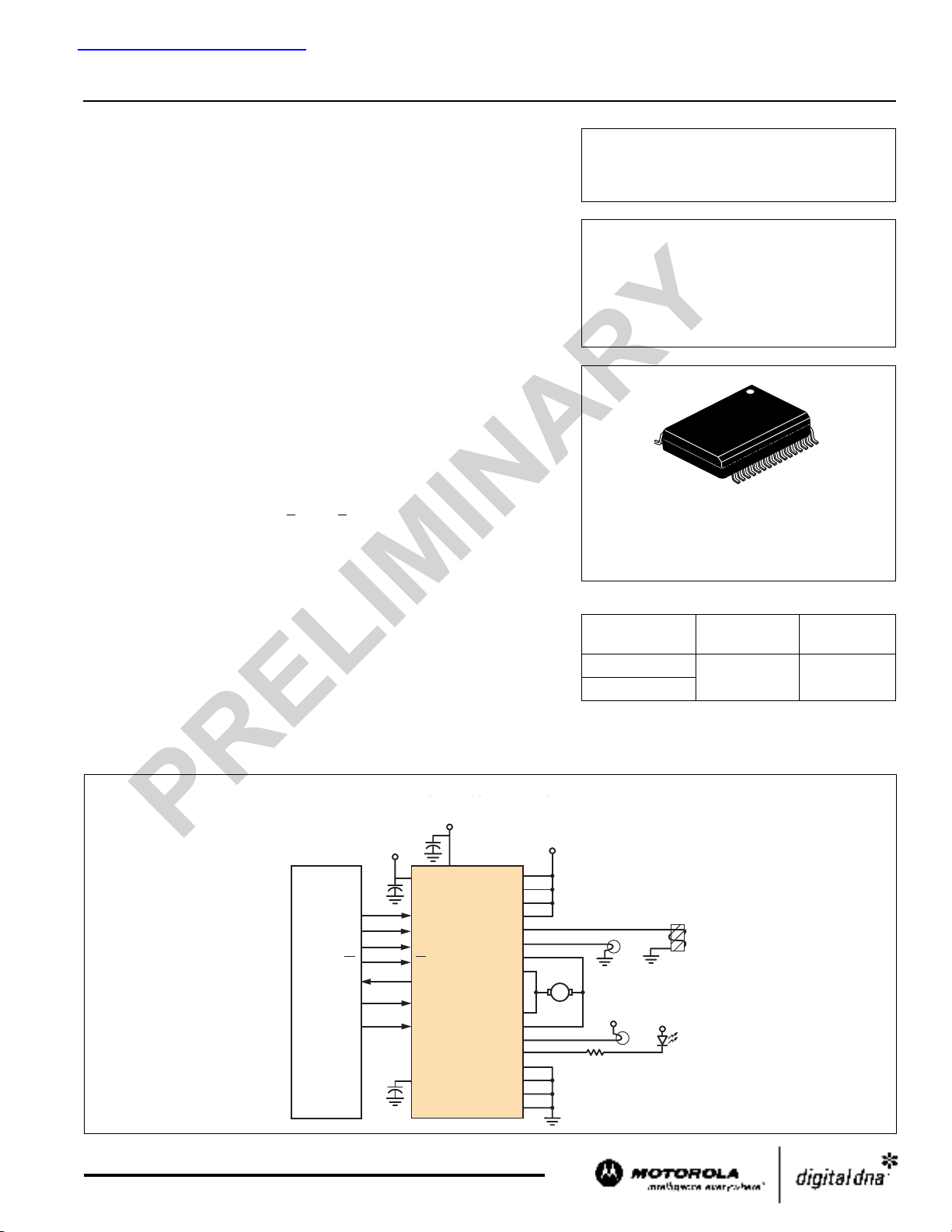
Configurable Octal Serial Switch
with Open Load Detect Current
Disable
The 33879 device is an 8-output hardware-configurable, high-side/low-side
switch with 16-bit serial input control. Two of the outputs may be controlled
directly via microprocessor for PWM applications. The 33879 incorporates
SMARTMOS technology, with CMOS logic, bipolar/MOS analog circuitry, and
DMOS power MOSFETs. The 33879 controls various inductive, incandescent,
or LED loads by directly interfacing with a microcontroller. The circuit’s
innovative monitoring and protection features include very low standby
currents, cascade fault reporting, internal +45 V clamp voltage for low-side
configuration, -20 V high-side configuration, output-specific diagnostics, and
nc...
independent overtemperature protection.
, I
Features
or
emiconduct
• Designed to Operate 5.5 V <
• 16-Bit SPI for Control and Fault Reporting, 3.3 V/ 5.0 V Compatible
• Outputs Are Current Limited (0.5 A to 1.0 A) to Drive Incandescent
Lamps
• Output Voltage Clamp, +45 V (Low Side) and -20 V (High Side) During
Inductive Switching
• On/Off Control of Open Load Detect Current (LED Application)
• Internal Reverse Battery Protection on V
• Loss of Ground or Supply Will Not Energize Loads or Damage IC
• Maximum 5.0 µA I
•R
• Short Circuit Detect and Current Limit with Automatic Retry
• Independent Overtemperature Protection
• Motorola Now Offers Pb-Free Packaging with the Suffix EK
of 1.0 Ω at 25°C Typical
DS(ON)
PWR
V
< 26.5 V
PWR
PWR
Standby Current at 13.0 V V
PWR
Document order number: MC33879
Rev 3.0, 06/2004
33879
CONFIGURABLE OCTAL SERIAL
SWITCH WITH OPEN LOAD
DETECT CURRENT DISABLE
EK (Pb-FREE) SUFFIX
DWB SUFFIX
CASE 1437-01
32-LEAD SOICW-EP
ORDERING INFORMATION
Device
PC33879DWB/R2
PC33879EK/R2
Temperature
Range (T
-40°C to 125°C
)
A
Package
32 SOICW-EP
Simplified Application Diagram
33879 Simplified Application Diagram
eescale S
Fr
MCU
MOSI
SCLK
MISO
PWM1
PWM2
This document contains information on a product under development.
Motorola reserves the right to change or discontinue this product without notice.
© Motorola, Inc. 2004
For More Information On This Product,
+5.0 V
VDDV
A0
CS
EN
DI
SCLK
CS
DO
IN5
IN6
GND
Go to: www.freescale.com
V
PWR
PWR
33879
V
BAT
D1
D2
D3
D4
S1
S2
S3
S4
D5
D6
D7
D8
S5
S6
S7
S8
High-Side Drive
H-Bridge Configuration
M
Low-Side Drive
V
BAT
V
BAT
Freescale Semiconductor, Inc.
nc...
, I
or
emiconduct
eescale S
V
DD
__
CS
SCLK
DI
DO
EN
IN5
IN6
~50 µA
~110 kΩ
~50 µA
~50 µA
SPI and
Interface
Logic
SPI Bit 0
Enable
SPI Bit 4
IN5
Internal
Bias
Power Supply
Charge
Pump
, POR, SLEEP
OV
Typical of all 8 output drivers
TLIM
Gate
Drive
Control
Current
Limit
+
–
+
–
Open/Short
Comparator
TLIM
Gate
Drive
Control
Current
Limit
+
–
+
–
Open/Short
Comparator
~3.5 V Open/Short
Threshold
Overvoltage
Shutdown/POR
Sleep State
–
+
–
+
~3.5 V Open/Short
Threshold
Open
Load
Detect
Current
~80 µA
Open
Load
Detect
Current
~80 µA
V
PWR
GND
D1
D2
D3
D4
D7
D8
S1
S2
S3
S4
S7
S8
D5
D6
S5
S6
Drain
Outputs
Source
Outputs
Drain
Outputs
Source
Outputs
Fr
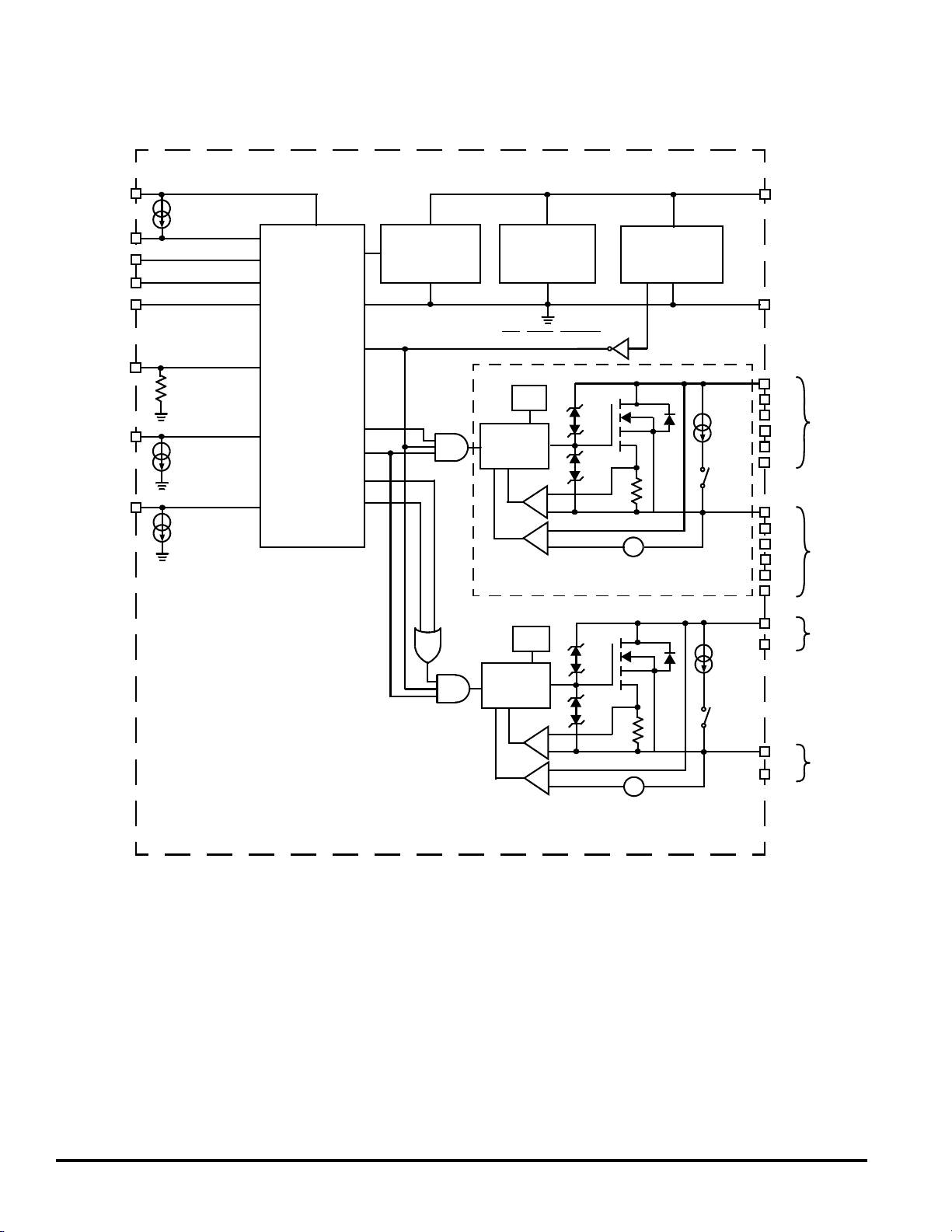
Figure 1. 33879 Simplified Internal Block Diagram
33879 MOTOROLA ANALOG INTEGRATED CIRCUIT DEVICE DATA
2
For More Information On This Product,
Go to: www.freescale.com
Freescale Semiconductor, Inc.
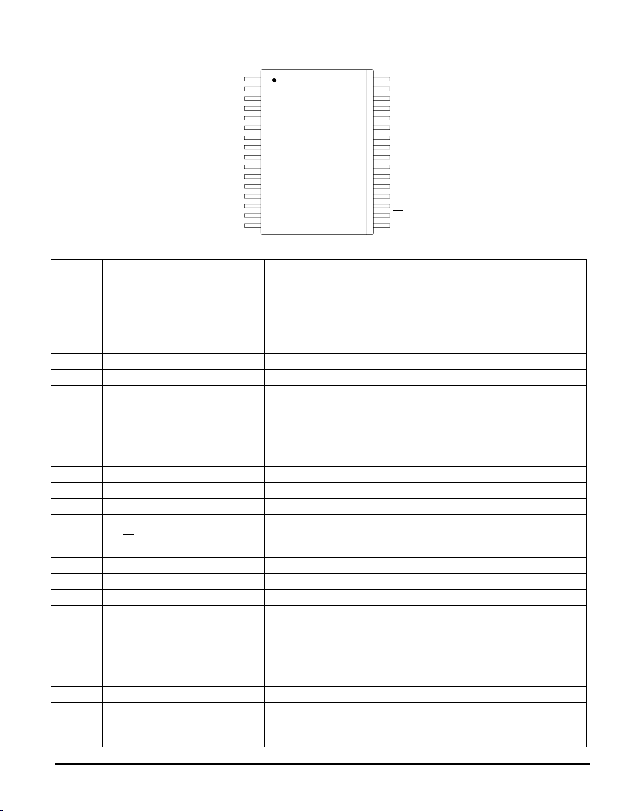
PIN FUNCTION DESCRIPTION
Pin Pin Name Formal Name Definition
nc...
, I
or
emiconduct
1GND
2V
3S8
4, 8, 9, 24,
25, 30
5D8
6S2
7D2
10 S1
11 D1
12 D6
13 S6
14 IN6
15 EN
16 SCLK
17 DI
18
NC
CS
eescale S
Fr
19 IN5
20 S5
21 D5
22 D3
23 S3
26 D4
27 S4
28 D7
29 S7
31 V
32 DO
PWR
DD
GND
V
DD
S8
NC
D8
S2
D2
NC
NC
S1
D1
D6
S6
IN6
EN
SCLK
Ground Digital ground.
Logic Supply Voltage Logic supply for SPI interface. With VDD low the device will be in sleep mode.
Source Output 8 Output eight MOSFET source pins.
Not Connected No internal connection to this pin.
Drain Output 8 Output eight MOSFETdrain pin.
Source Output 2 Output two MOSFET source pin.
Drain Output 2 Output two MOSFET drain pin.
Source Output 1 Output one MOSFET source pin.
Drain Output 1 Output one MOSFET drain pin.
Drain Output 6 Output six MOSFET drain pin.
Source Output 6 Output six MOSFET source pin.
Command Input 6 PWM direct control input pin for output 6. IN6 is “OR” with SPI bit.
Enable Input IC Enable. Active high. With EN low, the device is in sleep mode.
SPI Clock SPI control clock input pin.
Serial Data Input SPI control data input pin from MCU to the 33879. Logic [1] activates output.
SPI Chip Select SPI control chip select input pin from MCU to the 33879. Logic [0] allows data to be
Command Input 5 PWM direct control input pin for output 5. IN5 is “OR” with SPI bit.
Source Output 5 Output five MOSFET source pin.
Drain Output 5 Output five MOSFET drain pin.
Drain Output 3 Output three MOSFET drain pin.
Source Output 3 Output three MOSFET source pin.
Drain Output 4 Output four MOSFET drain pin.
Source Output 4 Output four MOSFET source pin.
Drain Output 7 Output seven MOSFET drain pin.
Source Output 7 Output seven MOSFET source pin.
Battery Input Power supply pin to the 33879. V
Serial Data Output SPI control data output pin from the 33879 to the MCU. DO=0 no fault, DO=1 specific
1
2
3
4
5
6
7
8
9
10
11
12
13
14
15
16
transferred in.
output has fault.
32
31
30
29
28
27
26
25
24
23
22
21
20
19
18
17
DO
V
PWR
NC
S7
D7
S4
D4
NC
NC
S3
D3
D5
S5
IN5
CS
DI
has internal reverse battery protection.
PWR
MOTOROLA ANALOG INTEGRATED CIRCUIT DEVICE DATA 33879
For More Information On This Product,
Go to: www.freescale.com
3

Freescale Semiconductor, Inc.
MAXIMUM RATINGS
All voltages are with respect to ground unless otherwise noted.
Rating Symbol Value Unit
Supply Voltage (Note 1) V
V
DD
CS, DI, DO, SCLK, IN5, IN6, and EN (Note 1) – -0.3 to 7.0 V
V
Supply Voltage (Note 1) V
PWR
Output Clamp Energy (Note 2) E
ESD Voltage
Human Body Model (Note 3)
Machine Model (Note 4)
Storage Temperature T
DD
PWR
CLAMP
V
ESD1
V
ESD2
STG
-0.3 to 7.0 V
-16 to 40 V
50 mJ
±2000
±200
-55 to 150
nc...
Operating Case Temperature T
C
-40 to 125
, I
Operating Junction Temperature T
or
Maximum Junction Temperature T
Power Dissipation (Note 5) P
Thermal Resistance
Junction-to-Ambient
Between the Die and the Exposed Die Pad
Notes
1. Exceeding these limits may cause malfunction or permanent damage to the device.
emiconduct
2. Maximum output clamp energy capability at 150
3. ESD1 testing is performed in accordance with the Human Body Model (C
4. ESD2 testing is performed in accordance with the Machine Model (C
5. Maximum power dissipation at T
= 25°C with no heatsink used.
A
°C junction temperature using single non-repetitive pulse method with I = 350 mA.
ZAP
= 200 pF, R
ZAP
J
J
D
R
JA
θ
R
JC
θ
= 100 pF, R
ZAP
= 1500 Ω).
ZAP
= 0 Ω).
-40 to 150
-40 to 150
1.7 W
71
1.2
DC
DC
DC
V
°C
°C
°C
°C
°C/W
eescale S
Fr
33879 MOTOROLA ANALOG INTEGRATED CIRCUIT DEVICE DATA
4
For More Information On This Product,
Go to: www.freescale.com
Freescale Semiconductor, Inc.
STATIC ELECTRICAL CHARACTERISTICS
Characteristics noted under conditions of 3.1 V ≤ V
Where applicable, typical values reflect the parameter’s approximate average value with V
Characteristic Symbol Min Typ Max Unit
POWER INPUT
Supply Voltage Range
Fully Operational
≤ 5.5 V, 5.5 V ≤ V
DD
V
PWR(fo)
≤ 18 V, -40°C ≤ TC ≤ 125°C unless otherwise noted.
PWR
5.5 – 26.5
= 13 V, TA = 25°C.
PWR
V
nc...
, I
or
emiconduct
Supply Current I
Sleep State Supply Current
V
or EN ≤ 0.8 V, V
DD
Sleep State Supply Current
EN ≤ 0.8 V, V
Overvoltage Shutdown Threshold Voltage V
V
PWR
V
Overvoltage Shutdown Hysteresis Voltage V
PWR
V
Undervoltage Shutdown Threshold Voltage V
PWR
Undervoltage Shutdown Hysteresis Voltage V
V
PWR
Logic Supply Voltage V
Logic Supply Current I
Logic Supply Sleep State Threshold Voltage V
Logic Supply Sleep State Hysteresis (Note 6) V
Notes
6. This parameter is guaranteed by design but is not production tested.
= 5.5 V
DD
PWR
= 13 V
PWR(OV-hys)
PWR(
PWR(on)
I
PWR(ss)
I
VDD(
ss)
PWR(
OV)
PWR(
UV)
UV-hys)
DD
DD
DD(SS)
DD(SS-hys)
–1424mA
µA
–2.05.0
µA
–2.05.0
27 28.5 32 V
0.2 1.5 2.5 V
3.0 4.0 5.0 V
300 500 700 mV
3.1 – 5.5 V
250 400 700 µA
0.8 2.5 3.0 V
0.3 – 1.5 V
eescale S
Fr
MOTOROLA ANALOG INTEGRATED CIRCUIT DEVICE DATA 33879
For More Information On This Product,
Go to: www.freescale.com
5
Freescale Semiconductor, Inc.
STATIC ELECTRICAL CHARACTERISTICS (continued)
Characteristics noted under conditions of 3.1 V ≤ V
≤ 5.5 V, 5.5 V ≤ V
DD
≤ 18 V, -40°C ≤ TC ≤ 125°C unless otherwise noted.
PWR
Where applicable, typical values reflect the parameter’s approximate average value with V
Characteristic Symbol Min Typ Max Unit
POWER OUTPUT
Drain-to-Source ON Resistance
I
= 0.350 A, TJ = 125°C, V
OUT
= 0.350 A, TJ = 25°C, V
I
OUT
= 0.350 A, TJ = -40°C, V
I
OUT
PWR
PWR
PWR
= 13 V
= 13 V
= 13 V
R
DS (ON)
–
–
–
= 13 V, TA = 25°C.
PWR
–
1.0
–
1.4
Ω
–
–
Output Self Limiting Current High-Side and Low-Side Configurations I
Output Fault Detection Voltage Threshold (Note 7)
Outputs Programmed OFF
Output Fault Detection Current @ Threshold, High-Side Configuration
Outputs Programmed OFF
nc...
Output Fault Detection Current @ Threshold, Low-Side Configuration
Outputs Programmed OFF
, I
Output OFF Open Load Detection Current, High-Side Configuration
or
V
= 16 V, V
Drain
Output OFF Open Load Detection Current, Low-Side Configuration
= 16 V, V
V
Drain
Output Clamp Voltage Low-Side Drive
I
= 10 mA
D
Output Clamp Voltage High-Side Drive
= -10 mA
I
S
emiconduct
Output Leakage Current High-Side and Low-Side Configurations
= 0 V, V
V
DD
Output Leakage Current Low-Side Configuration
= 5.0 V, V
V
DD
Open Load Detection Current Disabled
Output Leakage Current High-Side Configuration
V
= 5.0 V, V
eescale S
Fr
DD
Open Load Detection Current Disabled
Overtemperature Shutdown (Note 8) T
Overtemperature Shutdown Hysteresis (Note 8) T
Notes
7. Output fault detection thresholds with outputs programmed OFF. Output fault detect thresholds are the same for output open and shorts.
8. This parameter is guaranteed by design but is not production tested.
Drain
= 0 V, Outputs Programmed OFF
Source
= 0 V, Outputs Programmed OFF
Source
= 16 V, V
= 16 V, V
Drain
= 16 V, V
Drain
Source
Source
Source
= 0 V
= 0 V,
= 0 V,
OUT(LIM)
V
OUT(flt-th)
I
OUT(flt-th)
I
OUT(flt-th)
I
OCO
I
OCO
V
OC(LSD)
V
OC(HSD)
I
OUT(LKG)
I
OUT(LKG)
I
OUT(LKG)
LIM
LIM(hys)
0.5 – 1.0 A
2.5 3.5 4.2
35 55 70
20 30 50
65 100 160
40 75 135
40 45 55
-15 -20 -25
––7.0
–– 5
––20
155 – 185
5.0 10 15
µA
µA
µA
µA
µA
µA
µA
°C
°C
V
V
V
33879 MOTOROLA ANALOG INTEGRATED CIRCUIT DEVICE DATA
6
For More Information On This Product,
Go to: www.freescale.com
Freescale Semiconductor, Inc.
STATIC ELECTRICAL CHARACTERISTICS (continued)
Characteristics noted under conditions of 3.1 V ≤ V
≤ 5.5 V, 5.5 V ≤ V
DD
≤ 18 V, -40°C ≤ TC ≤ 125°C, unless otherwise noted.
PWR
Typical values, where applicable, reflect the parameter’s approximate average value with V
Characteristic Symbol Min Typ Max Unit
DIGITAL INTERFACE
Input Logic High-Voltage Thresholds (Note 9) V
Input Logic Low-Voltage Thresholds (Note 9) V
IN5, IN6, EN Input Logic Current
IN5, IN6, EN = 0 V
I
IN5, IIN6, IEN
IH
IL
0.7 x V
GND - 0.3 – 0.2 x V
-10 – 10
= 13 V, TA = 25°C
PWR
DD
–V
+ 0.3 V
DD
DD
V
µA
nc...
, I
or
emiconduct
eescale S
IN5, IN6 Pull-Down Current
0.8 V to 5.0 V
EN Pull-Down Current
EN = 5.0 V
SCLK, DI Input, Tri-State DO Output
0 V to 5.0 V
CS Input Current
CS = V
DD
CS Pull-Up Current
CS = 0 V
CS Leakage Current to V
CS = 5.0 V, V
DO High-State Output Voltage
I
DO-HIGH
DO Low-State Output Voltage
I
DO-LOW
Input Capacitance on SCLK, DI, Tri-State DO, IN5, IN6, EN (Note 10) C
Notes
9. Upper and lower logic threshold voltage levels apply to DI,
10. This parameter is guaranteed by design but not production tested.
DD
= -1.6 mA
= 1.6 mA
= 0 V
DD
CS, SCLK, IN5, IN6, and EN.
I
I
SCK, IDI, ITriDO
V
IN5, IIN6,
I
EN
I
CS
I
CS
I
CS(LKG)
DOHIGH
V
DOLOW
IN
30 45 100
30 45 100
-10 – 10
-10 – 10
-30 – -100
––10
VDD - 0.4 – V
––0.4
– – 20 pF
DD
µA
µA
µA
µA
µA
µA
V
V
Fr
MOTOROLA ANALOG INTEGRATED CIRCUIT DEVICE DATA 33879
For More Information On This Product,
Go to: www.freescale.com
7

Freescale Semiconductor, Inc.
DYNAMIC ELECTRICAL CHARACTERISTICS
Characteristics noted under conditions of 3.1 V ≤ V
≤ 5.5 V, 5.5 V ≤ V
DD
≤ 18 V, -40°C ≤ TC ≤ 125°C unless otherwise noted.
PWR
Where applicable, typical values reflect the parameter’s approximate average value with V
Characteristic Symbol Min Typ Max Units
POWER OUTPUT TIMING
= 13 V, TA = 25°C.
PWR
Output Slew Rate Low-Side Configuration (Note 11)
R
= 620 Ω, CL = 200 pF
LOAD
Output Slew Rate Low-Side Configuration (Note 11)
R
= 620 Ω, CL = 200 pF
LOAD
Output Rise Time High-Side Configuration (Note 11)
R
= 620 Ω, CL = 200 pF
LOAD
Output Fall Time High-Side Configuration (Note 11)
nc...
, I
Output Turn ON Delay Time, High-Side and Low-Side Configuration
(Note 12)
or
Output Turn OFF Delay Time, High-Side and Low-Side Configuration
(Note 12)
Output Fault Delay Time (Note 13)
Power-ON Reset Delay
Low-State Duration on V
emiconduct
Notes
11. Output slew rate respectively measured across a 620 Ω resistive load at 10 to 90 percent and 90 to 10 percent voltage points. C
12. Output turn ON and OFF delay time measured from 50 percent rising edge of
13. Duration of fault before fault bit is set. Duration between access times must be greater than 300 µs to read faults.
= 620 Ω, CL = 200 pF
R
LOAD
Delay Time Required from Rising Edge of EN and V
or EN for Reset
DD
or EN ≤ 0.2 V
V
DD
is connected from Drain or Source output to Ground.
to SPI Active
DD
t
SR(
)
rise
t
SR(
)
fall
t
SR(
rise
t
SR(
)
fall
t
DLY(on)
t
DLY(
off)
t
FAULT
t
POR
t
RESET
CS to the beginning of the 10 and 90 percent transition points.
0.1 0.5 1.0
0.1 0.5 1.0
)
0.1 0.3 1.0
0.1 0.3 1.0
1.0 15 50
1.0 30 100
100 – 300 µs
100 – –
100 – –
V/µs
V/µs
V/µs
V/µs
µs
µs
µs
µs
Capacitor
L
eescale S
Fr
33879 MOTOROLA ANALOG INTEGRATED CIRCUIT DEVICE DATA
8
For More Information On This Product,
Go to: www.freescale.com

Freescale Semiconductor, Inc.
DYNAMIC ELECTRICAL CHARACTERISTICS (continued)
Characteristics noted under conditions of 3.1 V ≤ V
Where applicable, typical values reflect the parameter’s approximate average value with V
Characteristic Symbol Min Typ Max Units
DIGITAL INTERFACE TIMING (Note 14)
≤ 5.5 V, 5.5 V ≤ V
DD
≤ 18 V, -40°C ≤ TC ≤ 125°C unless otherwise noted.
PWR
= 13 V, TA = 25°C.
PWR
nc...
, I
or
emiconduct
Recommended Frequency of SPI Operation (Note 14) f
Falling Edge of
Falling Edge of SCLK to Rising Edge of
DI to Falling Edge of SCLK (Required Setup Time) t
Falling Edge of SCLK to DI (Required Hold Time) t
DI,
CS, SCLK Signal Rise Time (Note 15)
DI,
CS, SCLK Signal Fall Time (Note 15)
Time from Falling Edge of
Time from Rising Edge of
Time from Rising Edge of SCLK to DO Data Valid (Note 18) t
Notes
14. This parameter is guaranteed by design. Production test equipment uses 4.16 MHz, 5.5V/3.1V SPI interface.
15. Rise and Fall time of incoming DI,
16. Time required for output status data to be available for use at DO pin.
17. Time required for output status data to be terminated at DO pin
18. Time required to obtain valid data out from DO following the rise of SCLK.
CS to Rising Edge of SCLK (Required Setup Time) t
CS (Required Setup Time) t
CS to DO Low Impedance (Note 16) t
CS to DO High Impedance (Note 17) t
CS, and SCLK signals suggested for design consideration to prevent the occurrence of double pulsing.
SPI
LEAD
LAG
DI(su)
DI(HOLD)
t
(DI)
r
t
(DI)
f
DO(EN)
DO(DIS)
VALID
–4.0 – MHz
100 – – ns
50 – – ns
16 – – ns
20 – – ns
–5.0 – ns
–5.0 – ns
– – 55 ns
– – 55 ns
–2555 ns
eescale S
Fr
MOTOROLA ANALOG INTEGRATED CIRCUIT DEVICE DATA 33879
For More Information On This Product,
Go to: www.freescale.com
9

Freescale Semiconductor, Inc.
Timing Diagrams
CS
SCLK
DI
DO
0.2 V
DD
t
lead
0.7 V
DD
0.2 V
DD
0.7 V
DD
0.2 V
DD
t
DO(en)
0.7 V
DD
0.2 V
DD
nc...
, I
or
VDD = 5.0 V
33879
SCLK
Under
Te st
emiconduct
NOTE: CL represents the total capacitance of the test
fixture and probe.
t
DI(su)tDI(hold)
MSB in
t
valid
MSB out LSB out
Figure 2. SPI Timing Diagram
SCLK
0.7 V
t
r(DI)
DD
< 50 ns
50%
DO
C
= 200 pF
L
DO
(Low-to-High)
DO
(High-to-Low)
0.2 V
0.7 V
DD
DD
t
r(DO)
t
lag
t
DO(dis)
t
f(DI)
< 50 ns
3.3/5.0 V
0.2 V
DD
0 V
t
valid
0.7 V
0.2 V
DD
DD
V
OH
V
OL
V
OH
V
OL
Figure 3. Valid Data Delay Time and Valid Time Test Circuit
eescale S
t
f(CS)
Fr
CS
0.2 V
DD
DO
(Tri-State to Low)
DO
(Tri-State to High)
<50 ns
t
t
Figure 4. Valid Data Delay Time and Valid Time Waveforms
t
r(CS)
<50 ns
90%
10%
DO(en)
90%
DO(en)
90%
10%
0.7 V
t
DO(dis)
t
DD
10%
DO(dis)
3.3/5.0 V
0 V
V
Tri-State
V
V
V
Tri-State
OL
OH
Figure 5. Enable and Disable Time Waveforms
33879 MOTOROLA ANALOG INTEGRATED CIRCUIT DEVICE DATA
10
For More Information On This Product,
Go to: www.freescale.com

Freescale Semiconductor, Inc.
Typical Electrical Characteristics
nc...
, I
or
emiconduct
eescale S
Fr
20
V
@ 18 V
PWR
19
Pin (mA)
18
PWR
17
16
15
Current into V
14
PWR
I
7
14
V
6
12
Pin (µA)
Pin (uA)
5
10
PWR
PWR
4
8
3
6
2
4
Current into V
1
Current into V
2
PWR
I
PWR
I
Figure 7. Sleep State I
140
120
Pin (µA)
100
TA = 25°C
PWR
80
0 25 50 100 125-40 75-25
T
Ambient Temperature (°C)
A,
Figure 6. I
Sleep State I
@ 13 V
PWR
0 25 50 100 125-40 75-25
0 25 50 100 125-40 75-25
T
Ambient Temperature (°C)
A,
T
Ambient Temperature
vs. Temperature
PWR
versus Temperature
PWR
vs. Temperature
PWR
1.4
1.2
1.0
(Ω)
0.8
0.6
DS(ON)
R
0.4
Figure 9. R
1.4
1.2
1.0
0.8
(Ω)
0.6
DS(ON)
R
0.4
0.2
0
V
@ 13 V
PWR
High Side Drive
0 25 50 100 125-40 75-25
T
Ambient Temperature (°C)
A,
vs. Temperature at 350 mA
DS(ON)
TA = 25°C
High Side Drive
5 10152025
(V)
V
PWR
Figure 10. R
DS(ON)
vs. V
PWR
at 350 mA
60
40
Current into V
20
PWR
I
0
MOTOROLA ANALOG INTEGRATED CIRCUIT DEVICE DATA 33879
510152025
V
PWR
Figure 8. Sleep State I
PWR
vs. V
PWR
For More Information On This Product,
11
Go to: www.freescale.com

Freescale Semiconductor, Inc.
Typical Electrical Characteristics (continued)
140
V
@ 16 V
80
60
40
20
PWR
0 25 50 100 125-40 75-25
T
Ambient Temperature (°C)
A,
120
100
Open Load (µA)
OCO,
I
nc...
Figure 11. Open Load Detection Current at Threshold Figure 12. Open Load Detection Threshold vs.
, I
5.0
TA = 25°C
Open Load Detect Enabled
4.5
4.0
3.5
3.0
Open Load Threshold (V)
2.5
,
2.0
OUT(flt-th)
V
0
5 10152025
T
Ambient Temperature (°C)
A,
Temperature
or
emiconduct
eescale S
Fr
33879 MOTOROLA ANALOG INTEGRATED CIRCUIT DEVICE DATA
12
For More Information On This Product,
Go to: www.freescale.com

Freescale Semiconductor, Inc.
SYSTEM/APPLICATION INFORMATION
FUNCTIONAL PIN DESCRIPTION
CS
Pin
The system MCU selects the 33879 with which to
communicate through the use of the chip select
low on
CS enables the data output (DO) driver and allows data
to be transferred from the MCU to the 33879 and vice versa.
Data clocked into the 33879 is acted upon on the rising edge of
CS.
To avoid any spurious data, it is essential the high-to-low
transition of the CS signal occur only when SPI clock (SCLK) is
in a logic low state.
SCLK Pin
nc...
, I
or
The SCLK pin clocks the internal shift registers of the 33879.
The serial data input (DI) pin is latched into the input shift
register on the falling edge of the SCLK. The serial data output
(DO) pin shifts data out of the shift register on the rising edge of
the SCLK signal. False clocking of the shift register must be
avoided to ensure validity of data. It is essential that the SCLK
pin be in a logic low state when the
For this reason, it is recommended the SCLK pin is commanded
to a logic low state when the device is not accessed (
high state). With
SCLK and DI are ignored and the DO output is tri-state.
CS in a logic high state, signals present on
CS pin makes any transition.
DI Pin
emiconduct
eescale S
Fr
The DI pin is used for serial instruction data input. DI
information is latched into the input register on the falling edge
of SCLK. A logic high state present on DI will program a specific
output on. The specific output will turn on with the rising edge of
the
CS signal. Conversely, a logic low state present on the DI
pin will program the output off. The specific output will turn off
with the rising edge of the
outputs and Open Load Detection Current on or off, send the DI
data beginning with the Open Load Detection Current bits,
followed by output eight, output seven, and so on to output one.
For each falling edge of the SCLK while
bit instruction (on or off) is loaded into the shift register per the
data bit DI state. Sixteen bits of entered information is required
to fill the input shift register.
CS signal. To program the eight
CS is logic low, a data
DO Pin
The DO pin is the output from the shift register. The DO pin
remains tri-state until the
on the 33879 device are reported as logic [1] through the DO
data pin. Regardless of the configuration of the driver, open
loads and shorted loads are reported as logic [1]. Conversely,
normal operating outputs with non-faulted loads are reported as
logic [0]. Outputs programmed with Open Load Detection
Current disabled will report logic [0] in the off state. The first
eight positive transitions of SCLK will report logic [0] followed by
the status of the eight output drivers. The DI / DO shifting of data
CS pin is in a logic low state. All faults
CS pin. Logic
CS in logic
follows a first-in, first-out protocol with both input and output
words transferring the most significant bit (MSB) first.
EN Pin
The EN pin on the 33879 enables the device. With the EN pin
high, output drivers may be activated and open/short fault
detection performed and reported. With the EN pin low, all
outputs become inactive, Open Load Detection Current is
disabled, and the device enters sleep mode. The 33879 will
perform Power-ON Reset on rising edge of the enable signal.
IN5 and IN6 Pins
The IN5 and IN6 command inputs allow outputs five and six
to be used in PWM applications. The IN5 and IN6 pins are
OR-ed with the Serial Peripheral Interface (SPI) command input
bits. For SPI control of outputs five and six, the IN5 and IN6 pins
should be grounded or held low by the microprocessor. When
using IN5 or IN6 to PWM the output, the control SPI bit must be
logic [0]. Maximum PWM frequency for each output is 2.0 kHz.
VDD Pin
The VDD input pin is used to determine logic levels on the
microprocessor interface (SPI) pins. Current from VDD is used
to drive DO output and the pull-up current for CS. VDD must be
applied for normal mode operation. The 33879 device will
perform Power-ON Reset with the application of V
V
Pin
PWR
The V
33879 IC. The V
All internal logic current is provided from the V
33879 will perform Power-ON Reset with the application of
V
PWR.
pin is battery input and Power-ON Reset to the
PWR
pin has internal reverse battery protection.
PWR
PWR
DD.
pin. The
D1–D8 Pins
The D1 to D8 pins are the open-drain outputs of the 33879.
For high-side drive configurations, the drain pins are connected
to battery supply. In low-side drive configurations, the drain pins
are connected to the low side of the load. All outputs may be
configured individually as desired. When configured as low-side
drive, the 33879 limits the positive inductive transient to 45 V.
S1–S8 Pins
The S1 to S8 pins are the source outputs of the 33879. For
high-side drive configurations, the source pins are connected
directly to the load. In low-side drive configurations, the source
is connected to ground. All outputs may be configured
individually as desired. When high-side drive is used, the 33879
will limit the negative inductive transient to negative 20 V.
MOTOROLA ANALOG INTEGRATED CIRCUIT DEVICE DATA 33879
For More Information On This Product,
13
Go to: www.freescale.com

Freescale Semiconductor, Inc.
MCU INTERFACE DESCRIPTION
Introduction
The 33879 is an 8-output hardware-configurable power
switch with 16-bit serial control. A simplified block diagram of
the 33879 is shown in Figure 1
The 33879 device uses high-efficiency up-drain power
DMOS output transistors exhibiting low drain-to-source ON
resistance (R
= 1.0 Ω at 25°C typical) and dense CMOS
DS(ON)
control logic. All outputs have independent voltage clamps to
provide fast inductive turn-off and transient protection.
In operation, the 33879 functions as an 8-output serial switch
serving as a MCU bus expander and buffer with fault
management and fault reporting features. In doing so, the
device directly relieves the MCU of the fault management
functions. This device directly interfaces to an MCU using a SPI
for control and diagnostic readout. Figure 13
nc...
basic SPI configuration between an MCU and one 33879.
, I
or
emiconduct
MC68HCxx
Microcontroller
Shift Register Shift Register
16 Bits
Receive
Buffer
Parallel
Ports
Figure 13. SPI Interface with Microcontroller
All inputs are compatible with 5.0 V and 3.3 V CMOS logic
levels and incorporate positive logic. When a SPI bit is
eescale S
programmed to a logic [0], the corresponding output will be
OFF. Conversely, when a SPI bit is programmed to logic [1] the
Fr
output being controlled will be ON. Diagnostics are treated in a
similar manner. Outputs with a fault will feed back (via DO) a
logic [1] to the microcontroller, while normal operating outputs
will provide a logic [0].
MOSI
MISO
on page 2.
DI
DO
SCLK
CS
illustrates the
33879
16 Bits
To
Logic
Figure 14
illustrates the daisy chain configuration using the
33879. Data from the MCU is clocked daisy chain through each
device while the
CS bit is commanded low by the MCU. During
each clock cycle, output status from the daisy chain is
transferred to the MCU via the Master In Slave Out (MISO) line.
On rising edge of
CS, command data stored in the input register
is then transferred to the output driver.
SCLK
Parallel Port
33879
CSSCLK SCLK
MC68HCxx
Microcontroller
with
SPI Interface
33879 33879
CS
MISO
DO DI DO DI DO DI
8 Outputs 8 Outputs 8 Outputs
MOSI
CS
Figure 14. 33879 SPI System Daisy Chain
Multiple 33879 devices can be controlled in a parallel input
fashion using the SPI. Figure 15 illustrates the control of
24 loads using three dedicated parallel MCU ports for chip
select.
DI
SCLK
DO
CS
DI
SCLK
DO
CS
DI
SCLK
DO
CS
33879
8 Outputs
33879
8 Outputs
33879
8 Outputs
MC68HCxx
Microcontroller
with
SPI Interface
Parallel
Ports
MOSI
SCLK
MISO
A
B
C
Figure 15. Parallel Input SPI Control
33879 MOTOROLA ANALOG INTEGRATED CIRCUIT DEVICE DATA
14
For More Information On This Product,
Go to: www.freescale.com

Freescale Semiconductor, Inc.
SPI DEFINITION
On each SPI communication, a 16-bit command word is sent
to the 33879 and a 16-bit status word is received from the
33879. The MSB is sent and received first. As Table 1
the Command Register defines the position and operation the
Table 1. Command Register Definition
MSB LSB
Bit 15 Bit 14 Bit 13 Bit 12 Bit 11 Bit 10 Bit 9 Bit 8 Bit 7 Bit 6 Bit 5 Bit 4 Bit 3 Bit 2 Bit 1 Bit 0
ON/ OFF
ON/ OFF
Open
Load
Detect
8
0 = Bits 0 to 7, Output commanded OFF.
0 = Bits 8 to 15, Open Load Detection Current OFF.
Open
Load
Detect
7
ON/ OFF
Open
Load
Detect
6
ON/ OFF
Open
Load
Detect
5
ON/ OFF
Open
Load
Detect
4
ON/ OFF
Open
Load
Detect
3
nc...
, I
MSB LSB
Bit 15 Bit 14 Bit 13 Bit 12 Bit 11 Bit 10 Bit 9 Bit 8 Bit 7 Bit 6 Bit 5 Bit 4 Bit 3 Bit 2 Bit 1 Bit 0
or
00000000OUT 8
0 = Bits 0 to 7, No Fault at Output.
1 = Bits 0 to 7, Output Short-to-Battery, Short-to-GND, Open Load,
or T
.
LIM
Serial Output (DO) Pin Reports
emiconduct
eescale S
Fr
Overtemperature Fault reported by serial output (DO) pin.
Overcurrent DO pin reports short to battery/supply or overcurrent condition.
Output ON Open Load Fault Not reported.
Output OFF Open Load Fault DO pin reports output OFF open load condition only with Open Load Detection Current enabled.
DO pin will report “0” for Output OFF Open Load Fault with Open Load Detection Current disabled.
Device Shutdowns
Overvoltage Total device shutdown at V
outputs assuming the previous state upon recovery from overvoltage.
Overtemperature Only the output experiencing an overtemperature shuts down. Output assumes previous state upon
recovery from overtemperature.
33879 will perform on rising edge of
shown in Table 2, defines the previous state status of the output
shows,
driver. Table 3
which the fault is communicated to the microprocessor.
ON/ OFF
Open
Load
Detect
2
ON/ OFF
Open
Load
Detect
1
ON/ OFF
ON/ OFF
OUT 8
OUT 7
1 = Bits 0 to 7, Output commanded ON.
1 = Bits 8 to 15 Open Load Detection Current ON.
Table 2. Fault Register Definition
Status
OUT 7
Status
Bits 8 to 15 will always return “0”.
Table 3. Fault Operation
= 27 V–30 V. Resumes normal operation with proper voltage. All
PWR
CS. The Fault Register,
identifies the type of fault and the method by
ON/ OFF
OUT 6
OUT 6
Status
ON/ OFF
OUT 5
OUT 5
Status
ON/ OFF
OUT 4
OUT 4
Status
ON/ OFF
OUT 3
OUT 3
Status
ON/ OFF
OUT 2
OUT 2
Status
ON/ OFF
OUT 1
OUT 1
Status
MOTOROLA ANALOG INTEGRATED CIRCUIT DEVICE DATA 33879
For More Information On This Product,
15
Go to: www.freescale.com

Freescale Semiconductor, Inc.
DEVICE OPERATION
Power Supply
The 33879 device has been designed with ultra-low sleep
mode currents. The device may enter sleep mode via the EN
pin or the V
current consumed by the V
Placing the 33879 in sleep mode resets the internal registers
to the Power-ON Reset state. The reset state is defined as all
outputs off and Open Load Detection Current disabled.
To place the 33879 in the sleep mode, either command all
outputs off and apply logic low to the EN input pin or remove
power from the V
device, it is recommended that all control inputs from the MCU
be low.
Paralleling of Outputs
nc...
Using MOSFETs as an output switch conveniently allows the
, I
paralleling of outputs for increased current capability. R
MOSFETs have an inherent positive temperature coefficient
or
that provides balanced current sharing between outputs without
destructive operation. This mode of operation may be desirable
in the event the application requires lower power dissipation or
the added capability of switching higher currents. Performance
of parallel operation results in a corresponding decrease in
R
DS(ON)
and the output current limits increase correspondingly.
Paralleling outputs from two or more different IC devices is
possible but not recommended.
emiconduct
Fault Logic Operation
Fault logic of the 33879 device has been greatly simplified
over other devices using SPI communications. As command
word one is being written into the shift register, a fault status
word is being simultaneously written out and received by the
MCU. Regardless of the configuration, with no outputs faulted
and Open Load Detection Current enabled, all status bits being
received by the MCU will be zero. When outputs are faulted (off
eescale S
state open circuit or on state short circuit / overtemperature), the
status bits being received by the MCU will be one. The
Fr
distinction between open circuit fault and short /
overtemperature is completed via the command word. For
example, when a zero command bit is sent and a one fault is
received in the following word, the fault is open /short-to-battery
for high-side drive or open/short-to-ground for low-side drive. In
the same manner, when a one command bit is sent and a one
fault is received in the following word, the fault is a short-toground/overtemperature for high-side drive or short-to-battery/
overtemperature for low-side drive. The timing between two
write words must be greater than 300 µs to allow adequate time
to sense and report the proper fault status.
pin. In the sleep mode (EN or VDD ≤ 0.8 V), the
DD
pin is less than 5.0 µA.
PWR
supply pin. Prior to removing VDD from the
DD
DS(ON)
while the output OFF Open Load Detection Currents
of
SPI Integrity Check
Checking the integrity of the SPI communication with the
initial power-up of the V
initial system start-up or reset, the MCU will write one 32-bit
pattern to the 33879. The first 16 bits read by the MCU will be
8 logic [0]s followed by the fault status of the outputs. The
second 16 bits will be the same bit pattern sent by the MCU. By
the MCU receiving the same bit pattern it sent, bus integrity is
confirmed. Please note the second 16-bit pattern the MCU
sends to the device is the command word and will be
transferred to the outputs with rising edge of
Important A SCLK pulse count strategy has been
implemented to ensure integrity of SPI communications. SPI
messages consisting of 16 SCLK pulses and multiples of
8 clock pulses thereafter will be acknowledged. SPI messages
consisting of other than 16 + multiples of 8 SCLK pulses will be
ignored by the device.
and EN pins is recommended. After
DD
CS.
Overtemperature Fault
Overtemperature detection and shutdown circuits are
specifically incorporated for each individual output. The
shutdown following an overtemperature condition is
independent of the system clock or any other logic signal. Each
independent output shuts down at 155
output shuts down owing to an overtemperature fault, no other
outputs are affected. The MCU recognizes the fault by a one in
the fault status register. After the 33879 device has cooled
below the switch point temperature and 15
output will activate unless told otherwise by the MCU via SPI to
shut down.
°C to 185°C. When an
°C hysteresis, the
Overvoltage Fault
An overvoltage condition on the V
device to shut down all outputs until the overvoltage condition
is removed. When the overvoltage condition is removed, the
outputs will resume their previous state. This device does not
detect an overvoltage on the V
threshold on the V
1.0 V typical hysteresis. A V
causing all outputs to be turned OFF.
Output OFF Open Load Fault
An output OFF open load fault is the detection and reporting
of an open load when the corresponding output is disabled
(input bit programmed to a logic low state). The Output OFF
Open Load fault is detected by comparing the drain-to-source
voltage of the specific MOSFET output to an internally
generated reference. Each output has one dedicated
comparator for this purpose.
pin is specified as 27 V to 30 V, with
PWR
pin. The overvoltage
DD
overvoltage detection is global,
PWR
pin will cause the
PWR
33879 MOTOROLA ANALOG INTEGRATED CIRCUIT DEVICE DATA
16
For More Information On This Product,
Go to: www.freescale.com

Freescale Semiconductor, Inc.
An output OFF open load fault is indicated when the drain-tosource voltage is less than the output threshold voltage
(V
OUT(
load open in the OFF state when the output drain-to-source
voltage is less than V
This device has an internal 80 µA current source connected
from drain to source of the output MOSFET. The current source
may be programmed on or off via SPI. The Power-ON Reset
state for the current source is “off” and must be enabled via SPI.
To achieve low sleep mode quiescent currents, the Open Load
Detection Current source of each driver is switched off when
V
DD
During output switching, especially with capacitive loads, a
false output OFF open load fault may be triggered. To prevent
this false fault from being reported, an internal fault filter of
100 µs to 300 µs is incorporated. A false fault reporting is a
function of the load impedance, R
as well as the supply voltage, V
nc...
triggers the built-in fault delay timer. The timer will time out
before the fault comparator is enabled and the fault is detected.
, I
Once the condition causing the open load fault is removed, the
or
device will resume normal operation. The open load fault,
however, will be latched in the output DO register for the MCU
to read.
) of 2.5 V to 4.0 V. Hence, the 33879 will declare the
)
flt-th
OUT(flt-th)
or EN is removed.
.
, C
DS(ON)
PWR
OUT
. The rising edge of CS
of the MOSFET,
Shorted Load Fault
A shorted load (overcurrent) fault can be caused by any
output being shorted directly to supply, or an output
experiencing a current greater than the current limit.
There are two safety circuits progressively in operation
during load short conditions that provide system protection:
emiconduct
1. The device’s output current is monitored in an analog
fashion using SENSEFET approach and current limited.
2. The device’s output thermal limit is sensed and when
attained causes only the specific faulted output to shut
down. The output will remain off until cooled. The device
will then reassert the output automatically. The cycle will
continue until fault is removed or the command bit
eescale S
Fr
instructs the output off. Shorted load faults will be
reported properly through SPI regardless of Open Load
Detection Current enable bits.
Undervoltage Shutdown
An undervoltage condition on VDD or V
shutdown of all outputs. The V
between 0.8 V and 3.0 V. V
between 3.0 V and 5.0 V. When the supplies fall below their
respective thresholds, all outputs are turned OFF. As both
supplies returns to normal levels, internal logic is reset and the
device resumes normal operation.
undervoltage threshold is
DD
undervoltage threshold is
PWR
will result in the
PWR
Output Voltage Clamp
Each output of the 33879 incorporates an internal voltage
clamp to provide fast turn-off and transient protection of each
output. Each clamp independently limits the drain-to-source
voltage to 45 V for low-side drive configurations and -20 V for
high-side drive configurations. The total energy clamped (E
can be calculated by multiplying the current area under the
current curve (I
Figure 16
Characterization of the output clamps, using a single pulse
non-repetitive method at 0.35 A, indicates the maximum energy
per output to be 50 mJ at 150°C junction temperature.
Drain-to-Source Clamp
Voltage (V
Drain Current
(I
D
Drain-to-Source ON
Voltage (V
Drain-to-Source ON
Voltage (V
Source Current
Source Clamp Voltage
(V
CL
) times the clamp voltage (VCL) (see
A
).
= 45 V)
CL
= 0.3 A)
)
DS(ON)
GND
)
DS(ON)
VS
GND
(IS = 0.3 A)
= -15 V)
Figure 16. Output Voltage Clamping
Current
Area (I
Current
Area (IA)
)
A
Drain Voltage
Clamp Energy
= IA x VCL)
(E
J
Clamp Energy
(E
= IA x VCL)
J
Source Voltage
Time
BAT
Time
)
J
SPI Configurations
The SPI configuration on the 33879 device is consistent with
other devices in the Octal Serial Switch (OSS) family. This
device may be used in serial SPI or parallel SPI with the 33298
and 33291. Different SPI configurations may be provided. For
more information, contact Motorola Analog Products Division or
local Motorola representative.
Reverse Battery
The 33879 has been designed with reverse battery
protection on the V
All outputs consist of a power MOSFET with an integral
substrate diode. During the reverse battery condition, current
will flow through the load via the substrate diode. Under this
circumstance, relays may energize and lamps will turn on.
Where load reverse battery protection is desired, a reverse
battery blocking diode must be placed in series with the load.
PWR
pin.
MOTOROLA ANALOG INTEGRATED CIRCUIT DEVICE DATA 33879
For More Information On This Product,
17
Go to: www.freescale.com

Freescale Semiconductor, Inc.
PACKAGE DIMENSIONS
EK (Pb-FREE) SUFFIX
32-LEAD SOIC WIDE BODY EXPOSED PAD
10.3
DWB SUFFIX
PLASTIC PACKAGE
CASE 1437-01
ISSUE O
nc...
, I
or
emiconduct
eescale S
7.6
7.4
1
PIN 1 ID
BB
16
5.15
2X 16 TIPS
0.3 A
B C
A
CC
A
0.3 A B C
5.3
4.7
C
32
17
B
95
4
11.1
10.9
9
0.25
0.19
ROTATED 90 CLOCKWISE
2.65
2.35
(0.29)
(0.203)
0.38
6
0.22
0.13MCAMB
SECTION A-A
°
30X
C
L
A
32X
BASE METAL
PLATING
0.65
SEATING
PLANE
0.10
8
NOTES:
1. ALL DIMENSIONS ARE IN MILLIMETERS.
2. DIMENSIONING AND TOLERANCING PER ASME
Y14.5M, 1994.
3. DATUMS B AND C TO BE DETERMINED AT THE PLANE
WHERE THE BOTTOM OF THE LEADS EXIT THE
PLASTIC BODY.
4. THIS DIMENSION DOES NOT INCLUDE MOLD FLASH,
PROTRUSION OR GATE BURRS. MOLD FLA SH,
PROTRUSION OR GATE BURRS SHALL NOT EXCEED
0.15 mm PER SIDE. THIS DIMENSION IS DETERMINED
AT THE PLANE WHERE THE BOTTOM OF THE LEADS
EXIT THE PLASTIC BODY.
5. THIS DIMENSION DOES NOT INCLUDE INTERLEAD
A
FLASH OR PROTRUSIONS. INTERLEAD FLASH AND
PROTRUSIONS SHALL NOT EXCEED 0.25 mm PER
SIDE. THIS DIMENSION IS DETERMINED AT THE
PLANE WHERE THE BOTTOM OF THE LEADS EXIT
THE PLASTIC BODY.
6. THIS DIMENSION DOES NOT INCLUDE DAMBAR
PROTRUSION. ALLOWABLE DA MBAR PROTRUSION
SHALL NOT CAUSE THE LEAD WIDTH TO EXCEED 0.4
mm PER SIDE. DAMBAR CANNOT BE LOCATED ON
THE LOWER RADIUS OR THE FOOT. MINIMUM SPACE
BETWEEN PROTRUSION AND ADJACENT LEAD
SHALL NOT LESS THAN 0.07 mm.
7. EXACT SHAPE OF EACH CORNER IS OPTIONAL.
8. THESE DIMENSIONS APPLY TO THE FLAT SECTION
OF THE LEAD BETWEEN 0.1 0 mm AND 0.3 mm FROM
THE LEAD TIP.
9. THE PACKAGE TOP MAY BE SMALLER THAN THE
PACKAGE BOTTOM. THIS DIMENSION IS
DETERMINED AT THE OUTERMOST EXTREMES OF
THE PLASTIC BODY EXCLUSIVE OF MOLD FLASH, TIE
BAR BURRS, GATE BURRS AND INTER-LEAD FLASH,
BUT INCLUDING ANY M ISMATCH BETWEEN THE TOP
AND BOTTOM OF THE PLASTIC BODY.
Fr
6.4
5.7
0.3 A B C
VIEW C-C
33879 MOTOROLA ANALOG INTEGRATED CIRCUIT DEVICE DATA
18
For More Information On This Product,
Go to: www.freescale.com
R0.08 MIN
0.25
GAUGE PLANE
°
8
°
0
°
0
MIN
0.9
0.5
SECTION B-B
0.1
0.0

Freescale Semiconductor, Inc.
NOTES
nc...
, I
or
emiconduct
eescale S
Fr
MOTOROLA ANALOG INTEGRATED CIRCUIT DEVICE DATA 33879
For More Information On This Product,
Go to: www.freescale.com
19

Freescale Semiconductor, Inc.
nc...
, I
or
emiconduct
eescale S
Fr
Information in this document is provided solely to enable system and software implementers to use Motorola products. There are no express or implied
copyright licenses granted hereunder to design or fabricate any integrated circuits or integrated circuits based on the information in this document.
Motorola reserves the right to make changes without further notice to any products herein. Motorola makes no warranty, representation or guarantee
regarding the suitability of its products for any particular purpose, nor does Motorola assume any liability arising out of the application or use of any product
or circuit, and specifically disclaims any and all liability, including without limitation consequential or incidental damages. “Typical” parameters which may be
provided in Motorola data sheets and/or specifications can and do vary in different applications and actual performance may vary over time. All operating
parameters, including “Typicals” must be validated for each customer application by customer’s technical experts. Motorola does not convey any license
under its patent rights nor the rights of others. Motorola products are not designed, intended, or authorized for use as components in systems intended for
surgical implant into the body, or other applications intended to support or sustain life, or for any other application in which the failure of the Motorola product
could create a situation where personal injury or death may occur. Should Buyer purchase or use Motorola products for any such unintended or
unauthorized application, Buyer shall indemnify and hold Motorola and its officers, employees, subsidiaries, affiliates, and distributors harmless against all
claims, costs, damages, and expenses, and reasonable attorney fees arising out of, directly or indirectly, any claim of personal injury or death associated
with such unintended or unauthorized use, even if such claim alleges that Motorola was negligent regarding the design or manufacture of the part.
MOTOROLA and the Stylized M Logo are registered in the US Patent and Trademark Office. All other product or service names are the property of their
respective owners.
© Motorola, Inc. 2004
HOW TO REACH US:
USA/EUROPE/LOCATIONS NOT LISTED: JAPAN: Motorola Japan Ltd.; SPS, Technical Information Center
Motorola Literature Distribution 3-20-1 Minami-Azabu. Minato-ku, Tokyo 106-8573, Japan
P.O. Box 5405, Denver, Colorado 80217 81-3-3440-3569
1-800-521-6274 or 480-768-2130
ASIA/PACIFIC: Motorola Semiconductors H.K. Ltd.; Silicon Harbour Centre
2 Dai King Street, Tai Po Industrial Estate, Tai Po, N.T., Hong Kong
852-26668334
HOME PAGE: http://motorola.com/semiconductors
For More Information On This Product,
Go to: www.freescale.com
MC33879

Copyright © Each Manufacturing Company.
All Datasheets cannot be modified without permission.
This datasheet has been download from :
www.AllDataSheet.com
100% Free DataSheet Search Site.
Free Download.
No Register.
Fast Search System.
www.AllDataSheet.com
 Loading...